Embed Size (px)
Citation preview

AW13412 Nov 2017 V1.1
www.awinic.com.cn 1 Copyright © 2017 SHANGHAI AWINIC TECHNOLOGY CO., LTD
0.1-3GHz SP2T Switch for 3G/4G TRX
FEATURES
Broadband frequency range: 0.1 to 3.0 GHz
Low insertion loss: 0.35dB typical @ 2.7 GHz
High isolation: >23dB @ 2.7 GHz
Integrated logic
Small DFN (6-pin, 1.1mm x 0.7 mm) package
(MSL1, 260 °C per JEDEC J-STD-020)
APPLICATIONS
Cellular 3G/4G TRX
Cellular modems , tablets and USB Devices
Other RF front-end modules
GENERAL DESCRIPTION
The AW13412 is a SP2T switch with low insertion
loss and high Isolation. It can be used to support
band switching and mode switching for cellular
3G/4G, data cards and tablets.
The symmetrical design of internal ports makes it
convenient for PCB routing and adjustment of
receiving and transmitting signals. The band/mode
switching is realized by the GPIO pins as
referenced in the chip block diagram and the
control logic.
The AW13412 is provided in a compact 1.1mm x
0.7mm, 6-pin DFN package.
TYPICAL APPLICATION CIRCUIT
RF1 RF2
ANT
4
VDD V1
1nF 100pF
AW13412
1
6
3
5
Figure 1 Typical Application Circuit of AW13412
All trademarks are the property of their respective owners.
AW13412 Nov 2017 V1.1
www.awinic.com.cn 2 Copyright © 2017 SHANGHAI AWINIC TECHNOLOGY CO., LTD
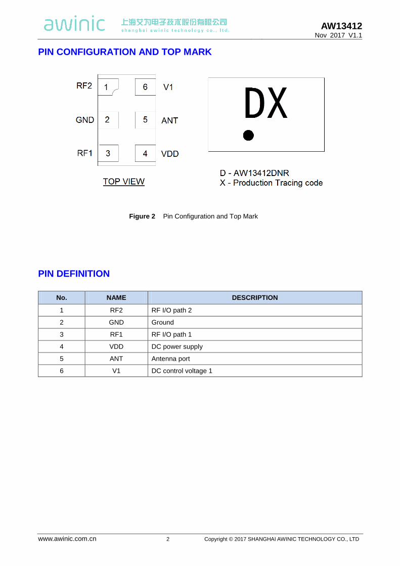
PIN CONFIGURATION AND TOP MARK
Figure 2 Pin Configuration and Top Mark
PIN DEFINITION
No. NAME DESCRIPTION
1 RF2 RF I/O path 2
2 GND Ground
3 RF1 RF I/O path 1
4 VDD DC power supply
5 ANT Antenna port
6 V1 DC control voltage 1

AW13412 Nov 2017 V1.1
www.awinic.com.cn 3 Copyright © 2017 SHANGHAI AWINIC TECHNOLOGY CO., LTD
FUNCTIONAL BLOCK DIAGRAM
Controller and Decoder
RF1
RF2
ANT
VDD V1 GND
Figure 3 FUNCTIONAL BLOCK DIAGRAM
ORDERING INFORMATION
Part Number Temperature Package Marking Moisture
Sensitivity Level
Environmental Information
Delivery Form
AW13412DNR
-40°C~85°C DFN 1.1mm*0.7mm-6L
DX MSL1 ROHS+HF
3000 units/
Tape and Reel
AW13412
Package Type
DN:DFN
Shipping
R:Tape & Reel
AW13412 Nov 2017 V1.1
www.awinic.com.cn 4 Copyright © 2017 SHANGHAI AWINIC TECHNOLOGY CO., LTD
ABSOLUTE MAXIMUM RATINGS(NOTE1)
PARAMETERS RANGE
Supply Voltage Range VDD 2.4V to 3.3V
Control Voltage Range V1 0V to 3V
RF input power(RF1/RF2) 34dBm
Operating Free-air Temperature Range -40°C to 85°C
Storage Temperature TSTG -55°C to 150°C
Lead Temperature (Soldering 10 Seconds) 260°C
ESD (NOTE 2)
HBM ±1000V
CDM ±500V
NOTE1: Conditions out of those ranges listed in "absolute maximum ratings" may cause permanent damages
to the device. In spite of the limits above, functional operation conditions of the device should within the
ranges listed in "recommended operating conditions". Exposure to absolute-maximum-rated conditions for
prolonged periods may affect device reliability.
NOTE2: The human body model is a 100pF capacitor discharged through a 1.5kΩ resistor into each pin. Test
method: MIL-STD-883J Method 3015.9
ELECTRICAL CHARACTERISTICS
VDD=2.8V, V1=0/1.8V, PIN=0dBm, TOP=+25℃, Z0=50Ω. (unless otherwise noted)
PARAMETER TEST CONDITION MIN TYP MAX UNIT
DC Specifications
VDD Supply Voltage 2.4 2.8 3 V
IDD Supply Current 45 A
VCTL_H VCTL_L
Control Voltage
High
Low
1.35
0
1.8
3
0.45
V
ICTL Control Current VCTL = 1.8V 0.1 1 A
tON Turn-on Switching Time
50% of final control voltage to 90% of final RF power, switching between RF1/2
0.5 1 S
RF Specifications
IL Insertion loss(ANT pin to RF1/RF2) 0.1-1.0G 1.0-2.0G 2.0-2.7G
0.30 0.45 0.35
0.40 0.55 0.45
dB dB dB
ISO Isolation (ANT pin to RF1/RF2) 0.1-1.0G 1.0-2.0G 2.0-2.7G
33 27 23
35 30 25
dB dB dB

AW13412 Nov 2017 V1.1
www.awinic.com.cn 5 Copyright © 2017 SHANGHAI AWINIC TECHNOLOGY CO., LTD
PARAMETER TEST CONDITION MIN TYP MAX UNIT
RL Input return loss (ANT pin to
RF1/RF2)
0.1-1.0G 1.0-2.0G 2.0-2.7G
23 20 18
27 22 20
dB dB dB
2fo Second harmonics (ANT pin to RF1/RF2)
PIN=+26dBm,
0.1-3GHz 85 dBc
3fo Third harmonics (ANT pin to
RF1/RF2)
PIN=+26dBm,
0.1-3GHz 88 dBc
P0.1dB 0.1dB Compression Point (ANT pin
to RF1/RF2) 0.1GHz–3GHz 34 dBm
IIP3 3rd Order Input Intercept Point
@ 2.0GHz, PIN=+26dBm,
Δf=1MHz 57 dBm
TIMING DIAGRAM (POWER ON AND OFF SEQUENCE) It is very important that the user adheres to the correct power-on/off sequence in order to avoid
damaging the device. The control signal V1 should be set to 0V unless VDD is set in the operating voltage
range.
Power ON:
1) Apply voltage supply --- VDD
2) Set Controls---V1
3) Apply RF input
Change switch position from one RF port to another:
1) Remove RF input
2) Change control voltages V1 to set the switch to desired RF port
3) Apply RF input
Power OFF:
1) Remove RF input
2) Remove control voltages-V1
3) Remove VDD input
VDD
V1
RF_IN
Power on Change switch Power Off
Figure 4 Power on/Change switch/Power off sequence

AW13412 Nov 2017 V1.1
www.awinic.com.cn 6 Copyright © 2017 SHANGHAI AWINIC TECHNOLOGY CO., LTD
AW13412 CONTROL LOGIC
State Active Path V1
0 ANT to RF1 0
1 ANT to RF2 1
APPLICATION CIRCUITS
RF1 RF2
ANT
4
VDD VCTL
1nF 100pF
AW13412
1
6
3
5
Figure 5 AW13412 EVB Schematic
Figure 6 AW13412 EVB
AW13412 Nov 2017 V1.1
www.awinic.com.cn 7 Copyright © 2017 SHANGHAI AWINIC TECHNOLOGY CO., LTD
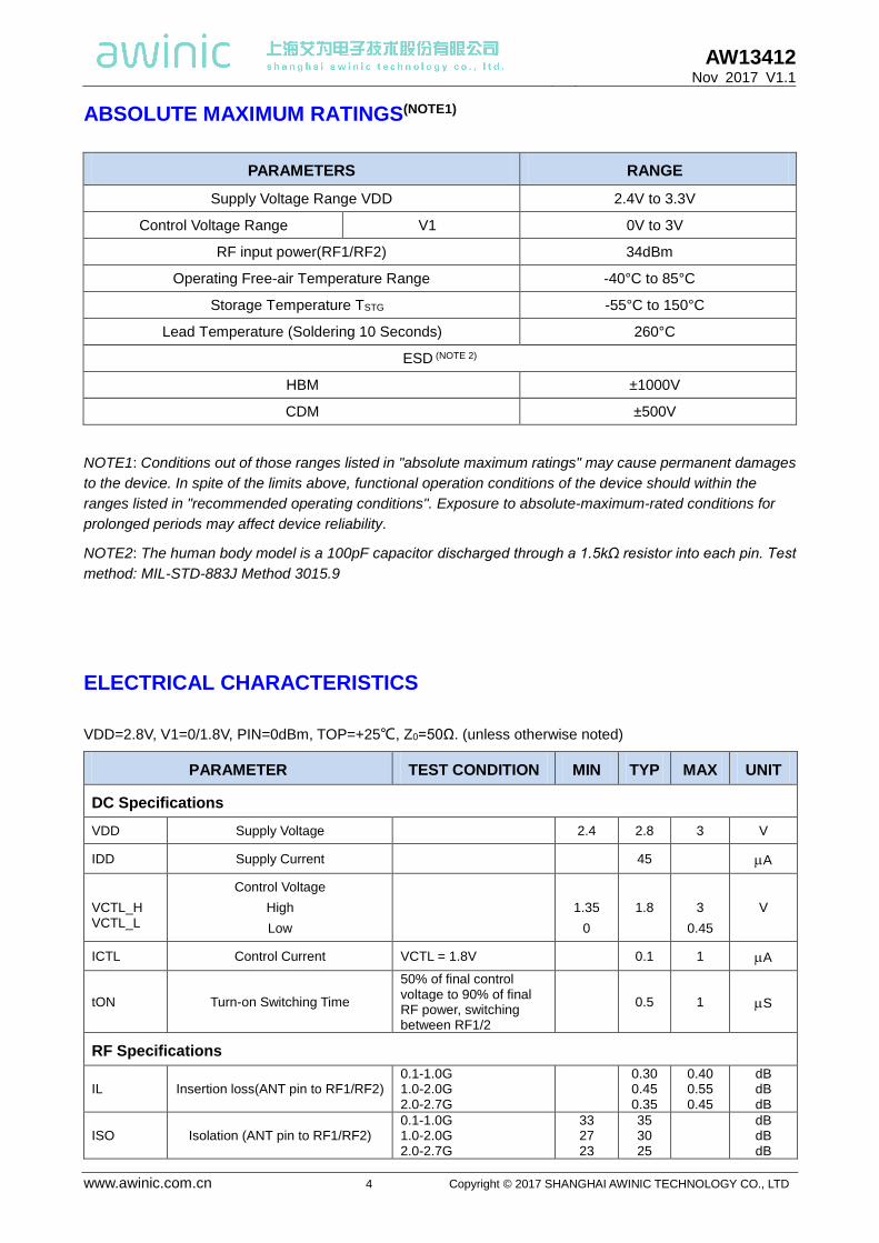
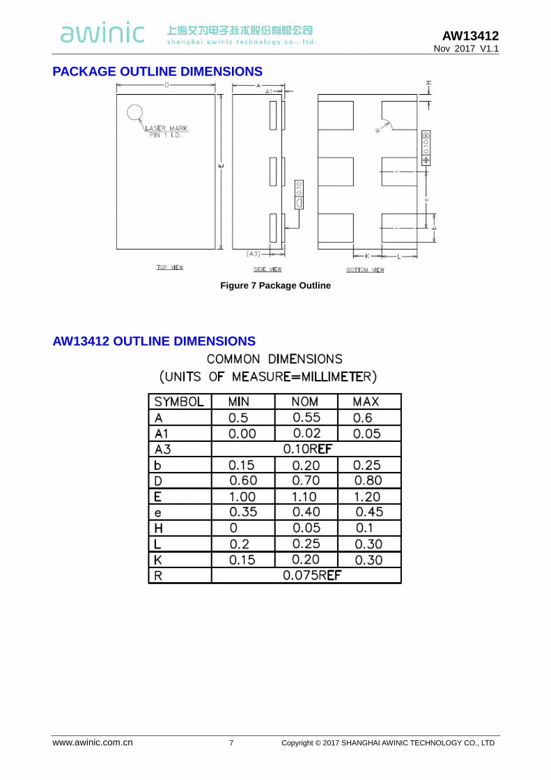
PACKAGE OUTLINE DIMENSIONS
Figure 7 Package Outline
AW13412 OUTLINE DIMENSIONS
AW13412 Nov 2017 V1.1
www.awinic.com.cn 8 Copyright © 2017 SHANGHAI AWINIC TECHNOLOGY CO., LTD
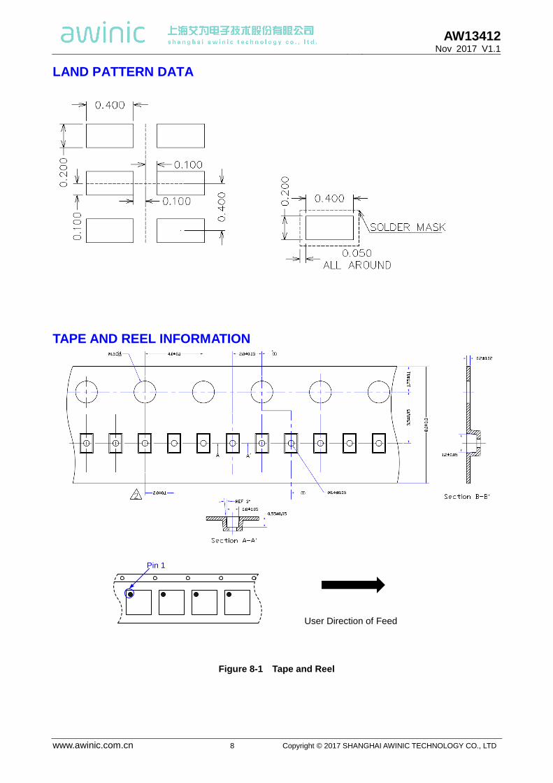
LAND PATTERN DATA
TAPE AND REEL INFORMATION
Pin 1
User Direction of Feed
Figure 8-1 Tape and Reel
AW13412 Nov 2017 V1.1
www.awinic.com.cn 9 Copyright © 2017 SHANGHAI AWINIC TECHNOLOGY CO., LTD
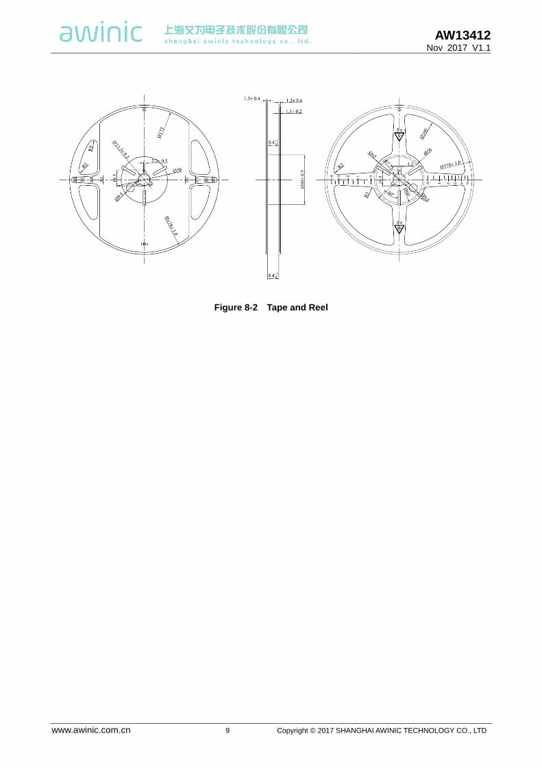
Figure 8-2 Tape and Reel
AW13412 Nov 2017 V1.1
www.awinic.com.cn 10 Copyright © 2017 SHANGHAI AWINIC TECHNOLOGY CO., LTD
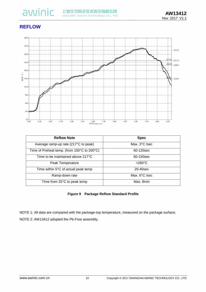
REFLOW
Reflow Note Spec
Average ramp-up rate (217°C to peak) Max. 3°C /sec
Time of Preheat temp. (from 150°C to 200°C) 60-120sec
Time to be maintained above 217°C 60-150sec
Peak Temperature >260°C
Time within 5°C of actual peak temp 20-40sec
Ramp-down rate Max. 6°C /sec
Time from 25°C to peak temp Max. 8min
Figure 9 Package Reflow Standard Profile
NOTE 1: All data are compared with the package-top temperature, measured on the package surface;
NOTE 2: AW13412 adopted the Pb-Free assembly.
AW13412 Nov 2017 V1.1
www.awinic.com.cn 11 Copyright © 2017 SHANGHAI AWINIC TECHNOLOGY CO., LTD
REVISION HISTORY
Vision Date Change Record
V1.0 Aug 2017 Officially Released
V1.1 Nov 2017 Change datasheet template
AW13412 Nov 2017 V1.1
www.awinic.com.cn 12 Copyright © 2017 SHANGHAI AWINIC TECHNOLOGY CO., LTD
DISCLAIMER
Information in this document is believed to be accurate and reliable. However, Shanghai AWINIC Technology
Co., Ltd (AWINIC Technology) does not give any representations or warranties, expressed or implied, as to
the accuracy or completeness of such information and shall have no liability for the consequences of use of
such information.
AWINIC Technology reserves the right to make changes to information published in this document, including
without limitation specifications and product descriptions, at any time and without notice. Customers shall
obtain the latest relevant information before placing orders and shall verify that such information is current and
complete. This document supersedes and replaces all information supplied prior to the publication hereof.
AWINIC Technology products are not designed, authorized or warranted to be suitable for use in medical,
military, aircraft, space or life support equipment, nor in applications where failure or malfunction of an
AWINIC Technology product can reasonably be expected to result in personal injury, death or severe property
or environmental damage. AWINIC Technology accepts no liability for inclusion and/or use of AWINIC
Technology products in such equipment or applications and therefore such inclusion and/or use is at the
customer’s own risk.
Applications that are described herein for any of these products are for illustrative purposes only. AWINIC
Technology makes no representation or warranty that such applications will be suitable for the specified use
without further testing or modification.
All products are sold subject to the general terms and conditions of commercial sale supplied at the time of
order acknowledgement.
Nothing in this document may be interpreted or construed as an offer to sell products that is open for
acceptance or the grant, conveyance or implication of any license under any copyrights, patents or other
industrial or intellectual property rights.
Reproduction of AWINIC information in AWINIC data books or data sheets is permissible only if reproduction
is without alteration and is accompanied by all associated warranties, conditions, limitations, and notices.
AWINIC is not responsible or liable for such altered documentation. Information of third parties may be subject
to additional restrictions.
Resale of AWINIC components or services with statements different from or beyond the parameters stated by
AWINIC for that component or service voids all express and any implied warranties for the associated
AWINIC component or service and is an unfair and deceptive business practice. AWINIC is not responsible or
liable for any such statements.