Embed Size (px)
Citation preview
1. INTRODUCTION
1.1 About circuit
From detectors to automobiles, audible alarms (also known to be called
buzzers) have become a part of our everyday life. Some of the uses of these alarms are
innocuous such as in a microwave oven. However, in some applications such as in a smoke
detector or medical equipment, a person’s life may depend upon the audible warning sound.
In all cases, the equipment designer should consider the desired characteristics of the
audible alarm at the initial design-planning phase to obtain satisfactory performance and
avoid costly redesign. The first characteristic for a designer to consider is the type of sound
such as a continuous, intermittent or specialty sound. Other critical criteria include sound
level, frequency, current draw, quality, mounting configuration, cost, and availability
1.2 Electromagnetic vs. Piezoelectric Alarm
Two main types of audible alarms are the electromagnetic type and the
piezoelectric type. Figure I show a summary of each type along with the different packages
available. The electromagnetic buzzer generally consists of a plastic housing with a metal
diaphragm that is flexed by an electromagnet. The main benefit of this design is the ability
to obtain low frequencies in a small package. Drawbacks include mechanical wear,
electrical noise, lower sound output, and large power consumption. The piezoelectric type
avoids electromechanical contacts by using a piezoelectric transducer. The transducer
consists of a polarized ceramic material bonded to a metal disc.
A voltage applied to the transducer will cause it toflex. A voltage that is applied and
released at an appropriate rate or frequency will produce a continuous audible sound.
Piezoelectric audible alarms offer no mechanical wear, an absence of electrical noise, low
power consumption, and a clear penetrating sound. Advances in transducer design have
allowed these devices to shrink in size and lower the sound frequency enabling them to
move into applications traditionally serviced by electromagnetic device
TIMER WTH AUDIBLE WARNING Page 1
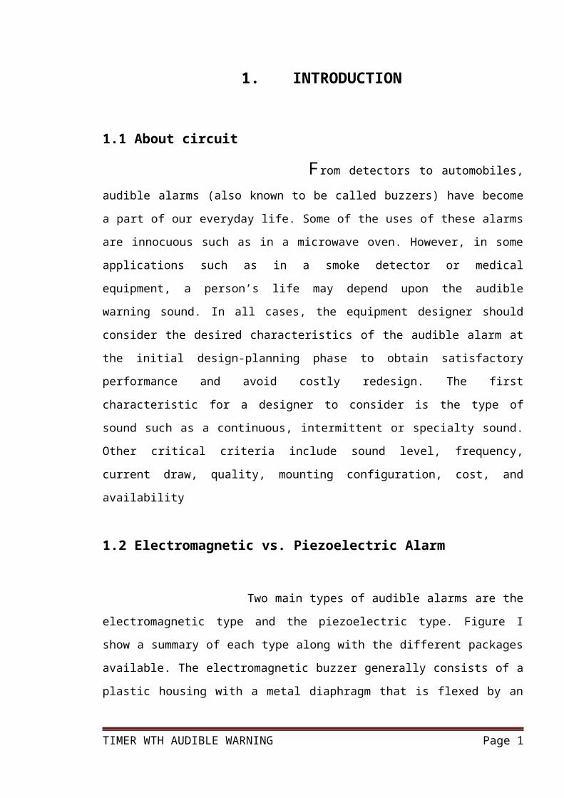
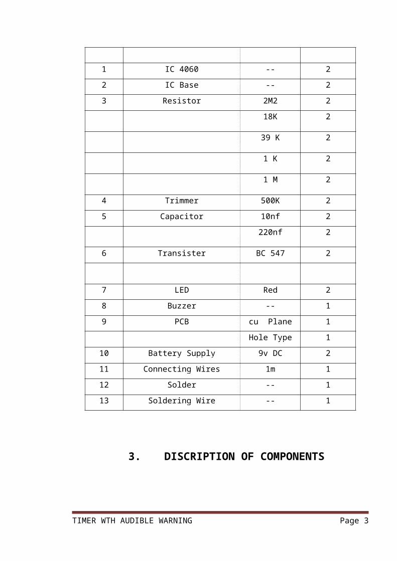
2. COMPONENT LIST
There are component which are used in making of the project circuit as given below
Table No 1 Componant Discription
Sr No Componant Name Value Quantity
1 IC 4060 -- 2
2 IC Base -- 2
3 Resistor 2M2 2
18K 2
39 K 2
1 K 2
1 M 2
4 Trimmer 500K 2
5 Capacitor 10nf 2
220nf 2
6 Transister BC 547 2
7 LED Red 2
8 Buzzer -- 1
9 PCB cu Plane 1
Hole Type 1
10 Battery Supply 9v DC 2
11 Connecting Wires 1m 1
12 Solder -- 1
13 Soldering Wire -- 1
TIMER WTH AUDIBLE WARNING Page 2
3. DISCRIPTION OF COMPONENTS
3.1 RESISTORS –
A Resistor is a heat-dissipating element and in the electronic circuits it is mostly
used for either controlling the current in the circuit or developing a voltage drop across it,
which could be utilized for many applications. There are various types of resistors, which
can be classified according to a number of factors depending upon:
(I) Material used for fabrication
(II) Wattage and physical size
(III) Intended application
(IV) Ambient temperature rating
(V) Cost
Basically the resistor can be split in to the following four parts from the construction
viewpoint.
(1) Base
(2) Resistance element
(3) Terminals
(4) Protective means.
The following characteristics are inherent in all resistors and may be controlled by
design considerations and choice of material i.e. Temperature co–efficient of resistance,
Voltage co–efficient of resistance, high frequency characteristics, power rating, tolerance &
voltage rating of resistors. Resistors may be classified as
(1) Fixed
(2) Semi variable
(3) Variable resistor.
In our project carbon resistors are being used.
TIMER WTH AUDIBLE WARNING Page 3
3.2 CAPACITORS:
The fundamental relation for the capacitance between two flat plates separated by a
dielectric material is given by:-
C=0.08854KA/D
Where: -
C= capacitance in pf.
K= dielectric constant
A=Area per plate in square cm.
D=Distance between two plates in cm
Design of capacitor depends on the proper dielectric material with particular type of
application. The dielectric material used for capacitors may be grouped in various classes
like Mica, Glass, air, ceramic, paper, Aluminum, electrolyte etc. The value of capacitance
never remains constant. It changes with temperature, frequency and aging. The capacitance
value marked on the capacitor strictly applies only at specified temperature and at low
frequencies.
3.3 LED (Light Emitting Diodes):
As its name implies it is a diode, which emits light when forward biased. Charge
carrier recombination takes place when electrons from the N-side cross the junction and
recombine with the holes on the P side. Electrons are in the higher conduction band on the
N side whereas holes are in the lower valence band on the P side. During recombination,
some of the energy is given up in the form of heat and light. In the case of semiconductor
materials like Gallium arsenide (GaAs), Gallium phoshide (Gap) and Gallium arsenide
TIMER WTH AUDIBLE WARNING Page 4
phoshide (GaAsP) a greater percentage of energy is released during recombination and is
given out in the form of light. LED emits no light when junction is reverse biased.
3.4 IC 4060
IC 4060 is an excellent integrated circuit for timing applications. Its ten active high
outputs can give time delay from few seconds to hours. With a few components, it is easy to
construct a simple but reliable time delay circuit.
IC 4060 is an Oscillator binary counter cum frequency divider. Its inbuilt oscillator
is based on three inverters. The basic frequency of the internal oscillator is determined by
the value of the capacitor connected to its pin 9 and that of the resistor in its pin 10. By
increasing or decreasing the value of capacitor / resistor, time delay can be changed. Each
output goes high after the completion of the timing cycle. To get maximum time period,
output Q10 is omitted in the IC itself so that double time is available between Q9 and Q11.
Inside the IC, there is an oscillator and 14 series connected bistables (Ripple cascade
arrangement). Internally the oscillator signal is applied to the first bistable which drives the
second bistable and so on. Since each bistable divides its input signal by two, a total of
fifteen signals are available, each of half the frequency of the previous one.
Ten of these fifteen signals are available on the output pins Q3- Q13.HEF 4060 is
CMOS version which can operate at 3 volts while CD 4060 is high voltage type that can
operate between 5 to 15 volts. It is necessary to add a capacitor close to pin 16 of IC so that
minute voltage changes will not affect the timing cycle. Reset pin 12 resets the timing cycle
once it is grounded. Outputs can give almost full supply voltage to drive light loads. Heavy
loads such as relay can be operated through a driver transistor. When the high output is
connected to the pin 11(clock input) through a diode, oscillation stops and IC remains
latched in high state till it resets. Pin 11 can be used to give clock pulses from an external
source.
TIMER WTH AUDIBLE WARNING Page 5
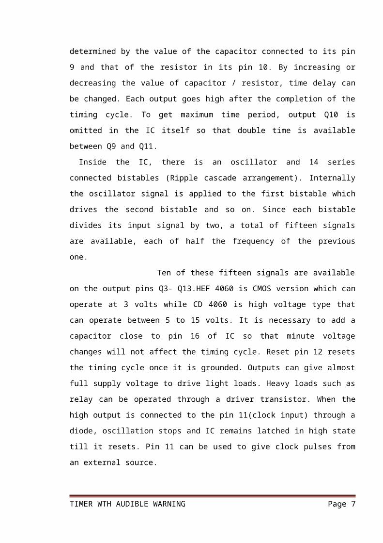
3.4.1 Functional Pin Diagram Of IC 4060
Fig 3.4.1 a)Functional Pin Diagram Of IC 4060
3.4.2 Pin outs of the IC 4066
Referring to the figure we see that the only input pins which require to be configured are
pin # 9, 10, 11, and 12, the all the remaining pin outs are the outputs of the IC.
The outputs are assigned for producing the time delays or the clock signals or the
oscillations or the frequency at different levels. Pin #7 generates the highest number of
frequencies for a set level, while pin #3 produces the least.
Therefore, suppose if pin # 7 generates a frequency of 1MHz, pin #5 will generate a
frequency of 500 Khz, pin # 4 generates 250 Khz, pin #6 generates 125KHz, pin #14
generates 62.5 KHz and so on, the frequency becomes half, in the order of the pin outs
7,5,4,6,14,13,15,1,2,3
TIMER WTH AUDIBLE WARNING Page 6
The above frequency or oscillations can be initiated by connecting a few passive
components at pin #9, 10 and 11 of the IC as shown in the figure, it’s that simple.
The variable resistor is used to vary the frequency to any desired level, the capacitor value
may also be altered for changing the frequency of the IC.
Pin #12 is the reset input and should always be grounded or connected to the negative
supply. A positive supply pulse to this input will reset the oscillations or revert the IC so
that it begins counting or oscillating from the beginning.
Pin #16 is the positive of the IC and pin #8 is the negative supply input of the IC.
3.5 BC547
A BC547 transistor is a negative-positive-negative (NPN) transistor that is used
for many purposes. Together with other electronic components, such as resistors, coils, and
capacitors, it can be used as the active component for switches and amplifiers. Like all other
NPN transistors, this type has an emitter terminal, a base or control terminal, and a collector
terminal. In a typical configuration, the current flowing from the base to the emitter controls
the collector current. A short vertical line, which is the base, can indicate the transistor
schematic for an NPN transistor, and the emitter, which is a diagonal line connecting to the
base, is an arrowhead pointing away from the base.
There are various types of transistors, and the BC547 is a bipolar junction
transistor (BJT). There are also transistors that have one junction, such as the junction field-
effect transistor, or no junctions at all, such as the metal oxide field-effect transistor
(MOSFET). During the design and manufacture of transistors, the characteristics can be
predefined and achieved. The negative (N)-type material inside an NPN transistor has an
excess of electrons, while the positive (P)-type material has a lack of electrons, both due to
a contamination process called doping.
3.6 Buzzer
TIMER WTH AUDIBLE WARNING Page 7
A buzzer or beeper is an audio signalling device, which may be mechanical,
electromechanical, or piezoelectric. Typical uses of buzzers and beepers include alarm
devices, timers and confirmation of user input such as a mouse click or keystroke.
3.6.1 Types Of Buzzers
1 Mechanical
2 Electromechanical
3 Piezoelectric
1-MechanicalA joy buzzer is an example of a purely mechanical buzzer.
2-Electromechanical Early devices were based on an electromechanical system identical to an electric
bell without the metal gong. Similarly, a relay may be connected to interrupt its own
actuating current, causing the contacts to buzz. Often these units were anchored to a wall or
ceiling to use it as a sounding board. The word "buzzer" comes from the rasping noise that
electromechanical buzzers made.
3-Piezoelectric beeper A piezoelectric element may be driven by an oscillating electronic circuit or other
audio signal source, driven with a piezoelectric audio amplifier. Sounds commonly used to
indicate that a button has been pressed are a click, a ring or a beep.
3.7 Trimmer
A trimmer or preset is a miniature adjustable electrical component. It is meant to be set
correctly when installed in some device, and never seen or adjusted by the device's user.
Trimmers can be variable resistors (potentiometers), variable capacitors, trimmable
inductors. They are common in precision circuitry like A/V components, and may need to
be adjusted when the equipment is serviced. Trimpots are often used to initially calibrate
TIMER WTH AUDIBLE WARNING Page 8
equipment after manufacturing. Unlike many other variable controls, trimmers are mounted
directly on circuit boards, turned with a small screwdriver and rated for many fewer
adjustments over their lifetime. Trimmers like trimmable inductors and trimmable
capacitors are usually found in superhet radio and television receivers, in the Intermediate
frequency, oscillator and RF circuits. They are adjusted into the right position during the
alignment procedure of the receiver.
Trimmers come in a variety of sizes and levels of precision. For example, multi-turn
trim potentiometers exist, in which it takes several turns of the adjustment screw to reach
the end value. This allows for very high degrees of accuracy
TIMER WTH AUDIBLE WARNING Page 9
4.OPERATING PRINCIPLE
A timing the timing alarm single board a led lattice module comprising a
circuit board is at least 16x15 patch double base colour led dot matrix circuit infrared
receiving head power supply interface is connected with the loudspeaker single chip
machine; Lattice circuit is set on the circuit board of the primary sight surface the upper
circuit board the back sight surface is set on the infrared receiving head power supply
interface is connected with the loudspeaker single chip machine; The single chip is
respectively connected with the dot matrix circuit infrared receiving head power supply
interface of speaker connected with the circuit board the back sight surface is also set on the
clock chip the clock chip is respectively connected with the single chip machine and power
supply interface is connected to the single chip machine input the data.
This utility model is controlled by single chip clock chip the speaker and a
matrix circuit can effectively improve the module the timing the timing alarm precision;
Can make the module it is convenient and flexible is set with the individuation of the timing
time and alarm multifunctional led dot matrix zhong also can be used for the timing time of
alarming effect is set in the module the displayed content of the background in the module
expands the application range.
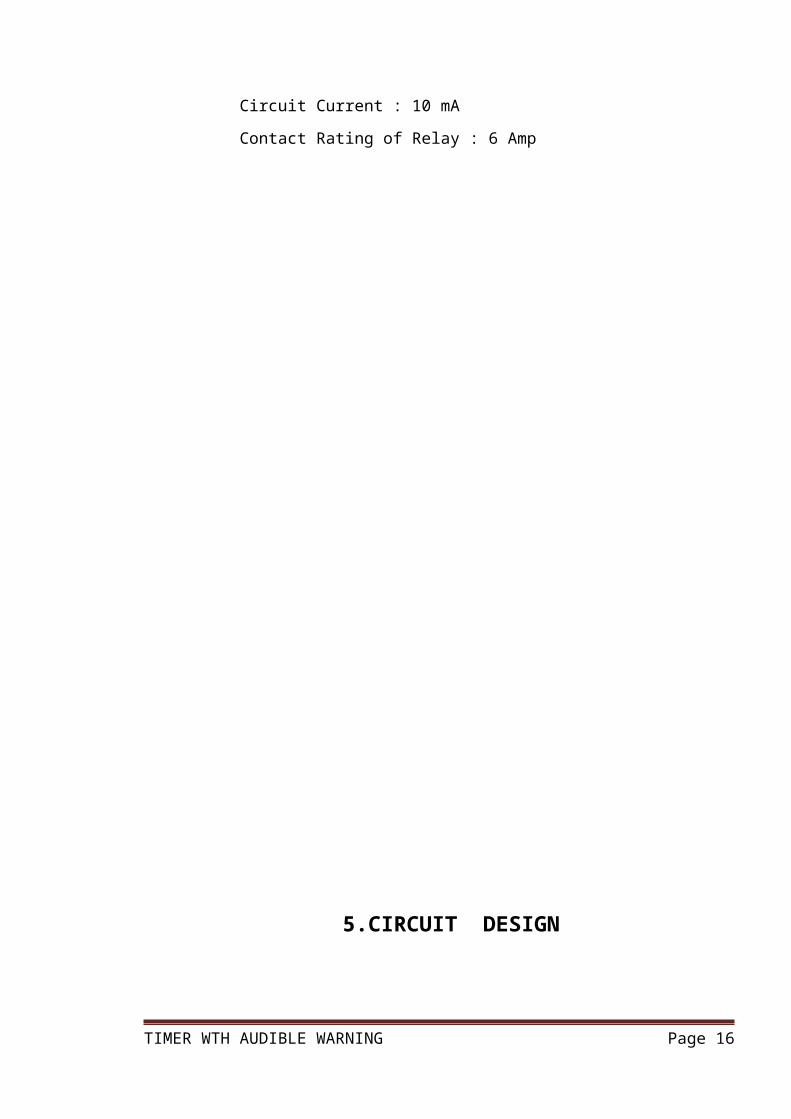
4.1 General Description Applications of this little circuit include a portable parking meter timer and
egg timer. The 14-stage binary ripple counter Type 4060, IC1, has an on chip oscillator
capable of stable operation over a relatively wide frequency range. In the present circuit, the
oscillator frequency is determined by an external RC network connected to pins 9, 10 and
11. When the circuit is switched on with S1, the pulse at junction R4-C2 resets the counter
and counting starts. When the count reaches bit 14 (Q13), pin 3 goes high so that the self-
oscillating piezo-electric buzzer, a 12 V type, is turned on via driver T1. The time delay is
set with the aid of P1. Time delays of between one minute and two hours Are possible by
appropriate dimensioning of the timing components:
TIMER WTH AUDIBLE WARNING Page 10
1-30 minutes : C1 = 220nF; P1 = 500kW
1-60 minutes : C1 = 470nF; P1 = 500kW
1-120 minutes : C1 = 470nF; P1 = 1MW
The timer is powered by a 9V pp3 battery. Lightemitting diode Dl does not
affect the operation of the circuit and is included merely to show that the timer works.
Diode Dl and resistor R3 are, therefore, optional components. A mercury tilt switch may be
used for S1 if the unit is to be used as a kitchen timer. The timer is then started by inverting
it like a sand-glass. With the buzzer actuated, the timer draws a current of about 10mA.
4.2 Technical Specifications - Characteristics Working voltage : 9V DC
Circuit Current : 10 mA
Contact Rating of Relay : 6 Amp
TIMER WTH AUDIBLE WARNING Page 11
5.CIRCUIT DESIGN
5.1 CIRCUIT DIAGRAM OF TIMER WITH AUDIBLE WARNING
Fig .5.1 CIRCUIT DIAGRAM OF TIMER WITH AUDIBLE WARNING
TIMER WTH AUDIBLE WARNING Page 12

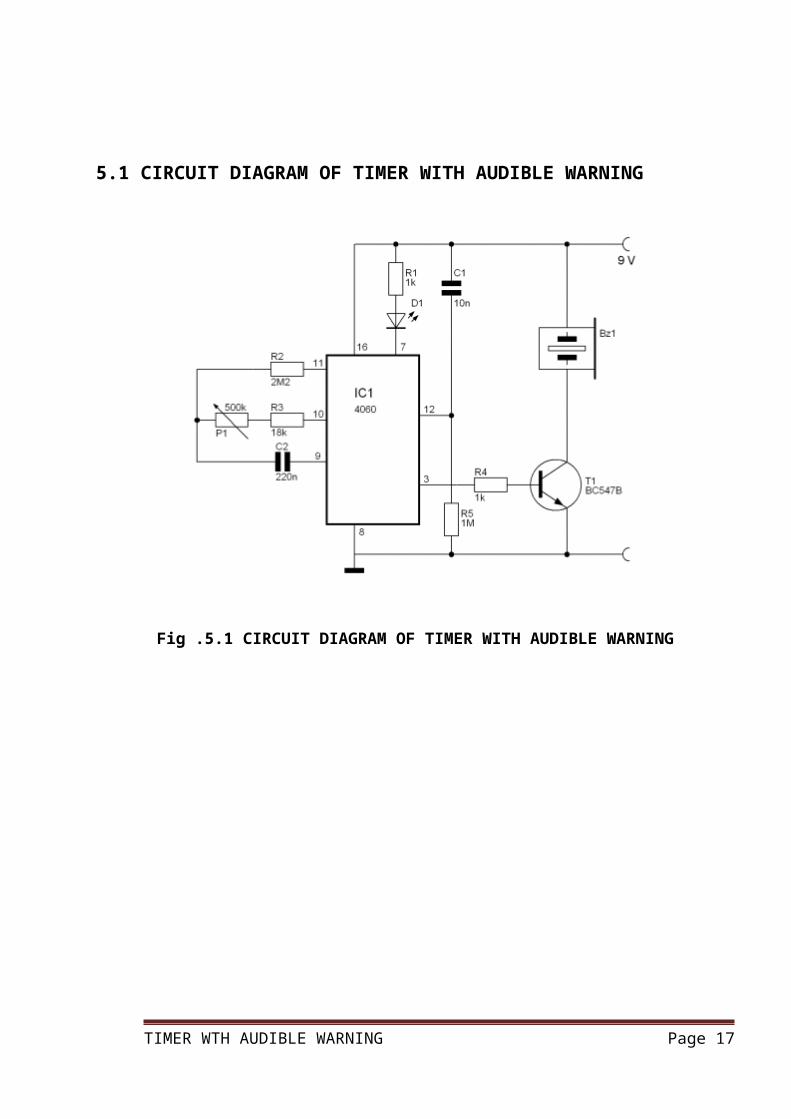
5.2 PCB LAYOUT :
Fig .5.2 PCB LAYOUT DIAGRAM OF TIMER WITH AUDIBLE WARNING
TIMER WTH AUDIBLE WARNING Page 13
6.WORKING
This timer circuit can set time at 1 minute to 2 hours.
First information, Technically, the IC 4060 is a 14-stage ripple carry binary counter,
the oscillator and divider of a monolithic integrated circuit, contained in a 16-pin dual-in-
line housing with ceramic or plastic. A phase of the integrated oscillator is a key feature of
the integrated circuit, which keeps the number of components in the integrated circuit to a
minimum at the design frequency generators or oscillators. The phase of the internal
oscillator operation easily through a network of resistors and a capacitor connected to the
pins #8, #9 and #10.
The timer time is determined by P1 and C1, through the following formula (seconds):
t = 2.3 * (P1 + 18k) * C1 * 2 ^ 13 .
The basic structure of the IC can be understood from the following:
According to the rules of standard CMOS ICs, all entries are first captured by
assigning them to specific business logic or simply a voltage (not exceeding the level of
supply voltage). For integrated circuit pin # 9, 10, 11 and 12 are active inputs. Resistance to
pin No. 11 can be considered a type of terminal or the reference resistance value that ideally
should be 10 times more than the resistor connected to the pin 10 (the combined value of
the resistor and pot fixed series).
The capacitor connected to pin # 9 is, in general, non-polar type.
TIMER WTH AUDIBLE WARNING Page 14
No Pin 12 is the reset input of the IC on the ground must be connected so that the IC
function (swing). This entry positive stop immediately IC to oscillate and return it to its
original state. Set the pen is connected to the ground of the integrated circuit for counting
(oscillate) for some time (for example, 1 minute), the connecting pin to the positive terminal
and to immediately stop the count reset to zero.
The rest of the pin-out, the outputs of the IC that generate oscillations specific
speeds. Costs are expressed in multiples of two for the entire chain pinouts as shown in the
diagram. Pin # 3 indicates the lowest frequency, the highest or pulses at time intervals while
the spindle 7 with the highest frequency or pulses having the lowest time intervals.
Basically the IC 4060 is a oscillator/Timer IC and can be used for producing
discretely variable accurate time intervals or delays or alternatively it may also be used as
an oscillator for acquiring high grade, accurate time period oscillations of frequencies.
TIMER WTH AUDIBLE WARNING Page 15
7.P.C.B. MANUFACTURING PROCESS
7.1 P.C.B.
It is an important process in the fabrication of electronic equipment. The design of
PCBs (Printed Circuit Boards) depends on circuit requirements like noise immunity,
working frequency and voltage levels etc. High power PCBs requires a special design
strategy.
The fabrication process to the printed circuit board will determine to a large
extent the price and reliability of the equipment. A common target aimed is the fabrication
of small series of highly reliable professional quality PCBs with low investment. The target
becomes especially important for customer tailored equipments in the area of industrial
electronics.
The layout of a PCB has to incorporate all the information of the board before one can go
on the artwork preparation. This means that a concept which clearly defines all the details of
the circuit and partly defines the final equipment, is prerequisite before the actual lay out
can start. The detailed circuit diagram is very important for the layout designer but he must
also be familiar with the design concept and with the philosophy behind the equipment.
7.2BOARD TYPES:
7.2.1 Single Sided Boards The single sided PCBs are mostly used in entertainment electronics where
manufacturing costs have to be kept at a minimum. However in industrial electronics cost
TIMER WTH AUDIBLE WARNING Page 16
factors cannot be neglected and single sided boards should be used wherever a particular
circuit can be accommodated on such boards.
7.2.2 Double Sided Boards
Double-sided PCBs can be made with or without plated through holes. The
production of boards with plated through holes is fairly expensive. Therefore plated through
hole boards are only chosen where the circuit complexities and density of components does
not leave any other choice.
7.3 CHRONOLOGY
The following steps have been followed in carrying out the project.
1. Study the books on the relevant topic.
2. Understand the working of the circuit.
3. Prepare the circuit diagram.
4. Prepare the list of components along with their specification.
5. Estimate the cost and procure them after carrying out market survey.
6. Plan and prepare PCB for mounting all the components.
7. Fix the components on the PCB and solder them.
8. Test the circuit for the desired performance.
9. Trace and rectify faults if any.
10. Give good finish to the unit.
TIMER WTH AUDIBLE WARNING Page 17
11. Prepare the project report
7.4DESIGN SPECIFICATION
7.4.1 PCB DESIGNING
The main purpose of printed circuit is in the routing of electric currents and signal
through a thin copper layer that is bounded firmly to an insulating base material sometimes
called the substrate. This base is manufactured with an integrally bounded layers of thin
copper foil which has to be partly etched or removed to arrive at a pre-designed pattern to
suit the circuit connections or other applications as required.
The term printed circuit board is derived from the original method where a printed
pattern is used as the mask over wanted areas of copper. The PCB provides an ideal
baseboard upon which to assemble and hold firmly most of the small components.
From the constructor’s point of view, the main attraction of using PCB is its role
as the mechanical support for small components. There is less need for complicated and
time consuming metal work of chassis contraception except perhaps in providing the final
enclosure. Most straight forward circuit designs can be easily converted in to printed wiring
layer the thought required to carry out the inversion cab footed high light an possible error
that would otherwise be missed in conventional point to point wiring .The finished project
is usually neater and truly a work of art.
Actual size PCB layout for the circuit shown is drawn on the copper board. The
board is then immersed in FeCl3 solution for 12 hours. In this process only the exposed
copper portion is etched out by the solution.
TIMER WTH AUDIBLE WARNING Page 18
Now the petrol washes out the paint and the copper layout on PCB is rubbed
with a smooth sand paper slowly and lightly such that only the oxide layers over the Cu are
removed. Now the holes are drilled at the respective places according to component layout
as shown in figure.
7.4.2 LAYOUT DESIGN
When designing the layout one should observe the minimum size (component body
length and weight). Before starting to design the layout we need all the required
components in hand so that an accurate assessment of space can be made. Other space
considerations might also be included from case to case of mounted components over the
printed circuit board or to access path of present components.
It might be necessary to turn some components around to a different angular
position so that terminals are closer to the connections of the components. The scale can be
checked by positioning the components on the squared paper. If any connection crosses,
then one can reroute to avoid such condition.
All common or earth lines should ideally be connected to a common line routed
around the perimeter of the layout. This will act as the ground plane. If possible try to route
the outer supply line to the ground plane. If possible try to route the other supply lines
around the opposite edge of the layout through the center. The first set is tearing the circuit
to eliminate the crossover without altering the circuit detail in any way.
Plan the layout looking at the topside to this board. First this should be translated inversely,
later for the etching pattern large areas are recommended to maintain good copper adhesion.
It is important to bear in mind always that copper track width must be according to the
recommended minimum dimensions and allowance must be made for increased width
where termination holes are needed. From this aspect, it can become little tricky to negotiate
the route to connect small transistors.
TIMER WTH AUDIBLE WARNING Page 19
There are basically two ways of copper interconnection patterns under side the
board. The first is the removal of only the amount of copper necessary to isolate the
junctions of the components to oneanother. The second is to make the interconnection
pattern looking more like conventional point wiring by routing uniform width of copper
from component to component.
7.4.3 ETCHING PROCESS
Etching process requires the use of chemicals. acid resistant dishes and running
water supply. Ferric chloride is mostly used solution but other etching materials such as
ammonium per sulphate can be used. Nitric acid can be used but in general it is not used
due to poisonous fumes.
The pattern prepared is glued to the copper surface of the board using a latex type of
adhesive that can be cubed after use. The pattern is laid firmly on the copper using a very
sharp knife to cut round the pattern carefully to remove the paper corresponding to the
required copper pattern areas. Then apply the resistant solution, which can be a kind of ink
solution for the purpose of maintaining smooth clean outlines as far as possible. While the
board is drying, test all the components.
Before going to next stage, check the whole pattern and cross check with the circuit
diagram. Check for any free metal on the copper. The etching bath should be in a glass or
enamel disc. If using crystal of ferric- chloride these should be thoroughly dissolved in
water to the proportion suggested. There should be 0.5 lt. of water for 125 gm of crystal.
To prevent particles of copper hindering further etching, agitate the solutions carefully by
gently twisting or rocking the tray.
The board should not be left in the bath a moment longer than is needed to remove
just the right amount of copper. Inspite of there being a resistive coating there is no
protection against etching away through exposed copper edges. This leads to over etching.
TIMER WTH AUDIBLE WARNING Page 20
Have running water ready so that etched board can be removed properly and rinsed. This
will halt etching immediately.
Drilling is one of those operations that calls for great care. For most purposes a
0.5mm drill is used. Drill all holes with this size first those that need to be larger can be
easily drilled again with the appropriate larger size.
7.4.4 COMPONENT ASSEMBLY
From the greatest variety of electronic components available, which runs into
thousands of different types it is often a perplexing task to know which is right for a given
job.
There could be damage such as hairline crack on PCB. If there are, then they can be
repaired by soldering a short link of bare copper wire over the affected part.
The most popular method of holding all the items is to bring the wires far apart after
they have been inserted in the appropriate holes. This will hold the component in position
ready for soldering.
Some components will be considerably larger .So it is best to start mounting the
smallest first and progressing through to the largest. Before starting, be certain that no
further drilling is likely to be necessary because access may be impossible later.
Next will probably be the resistor, small signal diodes or other similar size
components. Some capacitors are also very small but it would be best to fit these
afterwards. When fitting each group of components mark off each one on the circuit as it is
fitted so that if we have to leave the job we know where to recommence.
Although transistors and integrated circuits are small items there are good reasons
for leaving the soldering of these until the last step. The main point is that these components
TIMER WTH AUDIBLE WARNING Page 21
are very sensitive to heat and if subjected to prolonged application of the soldering iron,
they could be internally damaged.
All the components before mounting are rubbed with sand paper so that oxide
layer is removed from the tips. Now they are mounted according to the component layout.
7.4.5 SOLDERING: -
This is the operation of joining the components with PCB after this operation the
circuit will be ready to use to avoid any damage or fault during this operation following care
must be taken.
1. A longer duration contact between soldering iron bit & components lead can exceed the
temperature rating of device & cause partial or total damage of the device. Hence before
soldering we must carefully read the maximum soldering temperature & soldering time for
device.
2. The wattage of soldering iron should be selected as minimum as permissible for that
soldering place.
3 .To protect the devices by leakage current of iron its bit should be earthed properly.
4. We should select the soldering wire with proper ratio of Pb & Tn to provide the suitable
melting temperature.
TIMER WTH AUDIBLE WARNING Page 22
5. Proper amount of good quality flux must be applied on the soldering point to avoid dry
soldering.
8.ADVANTAGES OF THE CIRCUIT
-This circuit is very helpful where time management is required the time delay can be
adjusted by user requirement data
-This circuit is easy to design and the component are easily available in the market
-This circuit is operated on 9 v DC supply
-This circuit is small in size so it can be easily carry outside place
TIMER WTH AUDIBLE WARNING Page 23
9.DISADVANTAGES OF THE CIRCUIT
-This circuit is not suitable for more time related operation
-It can be operated on only AC supply only so after some day battery is discharge
-Time delay chaging process is complicated and some time not working
-Sound which is produce from the circuit some time irated user
TIMER WTH AUDIBLE WARNING Page 24
10.APPLICATION OF THE CIRCUIT
-This circuit is vary from 1 minute to 120 minute so it can be used in many places like time
related sport –chess, company alarm system ,In computer hardware system etc
-This circuit is used where time related operation are required
-Also this circuit is used in the fridge door alarm ,comuter printer ,mobile hardware system
etc
TIMER WTH AUDIBLE WARNING Page 25
11.PRECAUTIONS
1. The soldering iron being used for soldering of semiconductors should be of low
voltage.
2. While soldering semiconductors heat sinks should be used.
3. While soldering solder should not spread over the entire circuit and solder tip should
be sharp and smooth.
4. While mounting components their values should be visible.
5. Semiconductors and other polarized components should be mounted with correct
polarity.
TIMER WTH AUDIBLE WARNING Page 26
6. Time should be carefully observed while etching process takes place on the PCB.
12.REFERANCES
Referances List
-www.electrokit.com
-www.redcicuit.com
-Earl D. Gates (2000). Introduction to Electronics: A Practical Approach. Thomson Delmar
Learning. ISBN 0-7668-1698-2.
-A.S. Sedra and K.C. Smith (2004). Microelectronic circuits (Fifth ed.). New York: Oxford University
Press. pp. 397 and Figure 5.17. ISBN 0-19-514251-9.
TIMER WTH AUDIBLE WARNING Page 27
TIMER WTH AUDIBLE WARNING Page 28