Embed Size (px)
Citation preview
University of Tasmania
High-Performance Microcontroller-Based Transvector-Controlled Pulsewidth Modulator .. Induction Motor Drive
By: Dang Trung Nam Tien
Supervisor: Mr John Arneaud
\!\ o<:.
UY \1\lli
Project submitted in partial fulfilment of the requirements for the degree of Master of Technology in the Faculty of Engineering, the University of Tasmania,
Astralia, March 1996.

Abstract:
A fully digitalised transvector control PWM-IM drive system based on the M68HC11 microcontroller is described. The controller receives a digital speed command from a host computer via RS-232 interface. The feedback control system employs a transvector control technique to achieve a high dynamic performance in the estimated frequency range from 5 to 100 Hz. The PWM modulator utilises a computational intensive, uniformly sampled sine wave technique at low frequency region while a look-up table, pattern retrieval method base on the harmonic elimination optimal technique is utilised at high frequency region. The system hardware is mostly based on the programmable counters while system software is completely written in C++.

Acknowledgments.
I wish to express sincere thanks to my supervisor, Mr John Arneaund, for his continued support, encouragement, guidance and suggestion through the year. I am grateful to Mr Gregory The and Mr Quang Ha for their helpful suggestions and technical advice on high performance system design. I am also grateful to Mr Glenn Meyhew for many helpful suggestion and discussion on digital system design and implementation. Many thanks go to Mr Bernard Chenary and Mr Steve A very for their valuable assistance in the development of technical aspects of the project. My thanks also go to all the other members of staff of the Department of the Electrical and Electronics Engineering for their helps through the year.
.l .. v c
\ \
r '/ ,. (
() ( (.\ \ C' ~ ( :{ ~\ 'A t.tt (.(
I ' ' L,
\ /1
ii
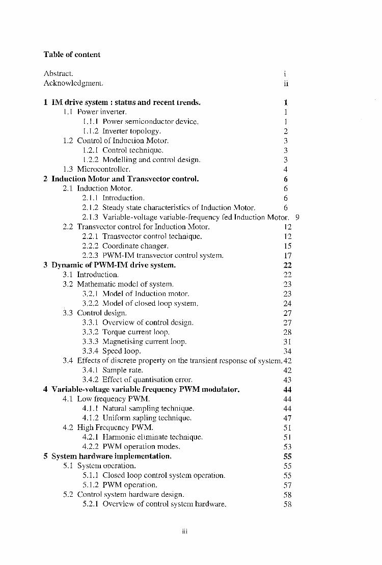
Table of content
Abstract. Acknowledgment. ii
1 IM drive system : status and recent trends. 1 1.1 Power inverter. 1
1.1.1 Power semiconductor device. 1 1.1.2 Inverter topology. 2
1.2 Control of Induction Motor. 3 1.2.1 Control technique. 3 1.2.2 Modelling and control design. 3
1.3 Microcontroller. 4 2 Induction Motor and Transvector control. 6
2.1 Induction Motor. 6 2.1.1 Introduction. 6 2.1.2 Steady state characteristics of Induction Motor. 6 2.1.3 Variable-voltage variable-frequency fed Induction Motor. 9
2.2 Transvector control for Induction Motor. 12 2.2.1 Transvector control technique. 12 2.2.2 Coordinate changer. 15 2.2.3 PWM-IM transvector control system. 17
3 Dynamic of PWM-IM drive system. 22 3.1 Introduction. 22 3.2 Mathematic model of system. 23
3.2.1 Model of Induction motor. 23 3.2.2 Model of closed loop system. 24
3.3 Control design. 27 3.3.1 Overview of control design. 27 3.3.2 Torque current loop. 28 3.3.3 Magnetising current loop. 31 3.3.4 Speed loop. 34
3.4 Effects of discrete property on the transient response of system. 42 3.4.1 Sample rate. 42 3.4.2 Effect of quantisation error. 43
4 Variable-voltage variable frequency PWM modulator. 44 4.1 Low frequency PWM. 44
4.1.1 Natural sampling technique. 44 4.1.2 Uniform sapling technique. 47
4.2 High Frequency PWM. 51 4.2.1 Harmonic eliminate technique. 51 4.2.2 PWM operation modes. 53
5 System hardware implementation. 55 5.1 System operation. 55
5 .1.1 Closed loop control system operation. 55 5.1.2 PWM operation. 57
5.2 Control system hardware design. 58 5 .2.1 Overview of control system hardware. 58
iii

5.2.2 M68HC11AO microcontroller. 5.2.3 Address latch. 5 .2.4 Data buffer. 5.2.5 Decoder. 5.2.6 EPROM memory. 5.2.7 RAM memory. 5.2.8 High speed oscillator. 5.2.9 16 bit down counter. 5.2.10 Monostable. 5 .2.11 Programmable 8 bit counter. 5 .2.12 Interrupt. 5 .2.13 Interfacing
5-3 Current and speed sensor. 5.3.1 Current sensor. 5.3.2 Speed sensor.
5.4 Power circuitry. 6 System software.
6.1 System software operation. 6.1.1 Selected mode procedure. 6.1.2 Speed procedure. 6.1.3 Current procedure. 6.1.4 PWM procedure. 6.1.5 Load delay time interrupt service routines 6.1.6 Control algorithm. 6.1.7 Processing time.
6.2 Software implementation in C++. 6.2.1 Direct access of peripheral device. 6.2.2 Interrupt programming. 6.2.3 Initialisation for external devices. 6.2.4 Communication programming.
7 Experimental results and evolution. 7.1 Experimental results. 7.2 Evolution and conclusion.
Principle Symbols. Selected references. Appendix A. Appendix B. Appendix C.
iv
59 61 61 62 64 64 66 66 68 68 69 70 70 72 72 72 73 75 75 76 76 76 76 78 78 79 79 79 80 80 83 83 88
The IM Drive System- Status and Recent Trends
Chapter 1 : The IM Drive System - Status and Recent Trends.
The technology of solid-state speed control of induction motor (IM) made great strides during the last decades. Traditionally, 1M were considered suitable for constant speed application though complex, inefficient and expensive methods of speed control were known before the advent of the solid-state era. For a long time, de motor were the workhorses in industry for adjustable speed applications. The induction motor, especially the cage type, seem to possess many distinct virtues in comparison with de machine. These relate to lower cost and weight, lower inertia, high efficiency, improved ruggedness and reliability to operate in a dirty and explosive environment due to the absence of commutators and brushes. Some of these virtues are of paramount importance, which makes the 1M drive mandatory in several areas of application. In spite of many virtues of IM, the cost of converters and complexity of control requirements are the main factors which are impeding the widespread application of 1M drives in competition with de drives. Therefore, the project intentionally starts with some discussion of the status and recent trends of IM drive system.
1-1, Power inverter : 1-1-1, Power semiconductor device : The power semiconductor device is the heart of the power inverter. The first invention of the power semiconductor device were the thyristor in the last 1950's. Gradually, other types, such as triac, gate turn - off thyristor (GTO's), bipolar power transistor (BJT's), power MOS field-effect transistor (MOSFET's), insulated gate bipolar transistor (IGBT's), static induction transistor (SIT's) and MOS-controlled thyristor (MCT's) were introduce. In parallel with the new device evolution, the power rating and switching performance of the existing devices began improving dramatically. + Thyristor have traditionally been the workhorse in power inverter. Starting originally with the C35 type (800V, 35A) introduced by GE, the modern lighttriggered high-power thyristor (6kV, 35kA) have been involving for more than three decades during the thyristor era. The thyristor application is common ranging from several watts to multimegawatt converter. + Triac or bidirectional thyristor were invented by GE almost immediately after thyristor commercialisation and found tremendous popularity for medium power inverter. Except for zero voltage ac line switching, the role of the triac will diminish in the future. + The GTO, which is another invention of GE that appeared at almost the same time as the triac, was a glimmer of hope, but soon, its research and application were abandoned, considering that device practically has no future. However, from the late 1970's and early 1980's, a number of Japanese corporations introduced high-power GTO's in the market and substantiated that voltage-fed inverters built with selfcontrolled GTO's have considerable efficiency, size, and reliability advantages over those with force-commutated thyristor. However, the GTO has large switching loss and shows a second breakdown problem at turn-off that demands a large turn-off snubber. The loss consideration also restricts switching frequency typically below one kHz. + Bipolar and field-effect transistor principles were known from the beginning of the solid-state era, but the modern power BJT's and MOSFET's penetrated the market from the mid 1970's. Darlington power transistor modules with built-in feedback
The IM Drive System- Status and Recent Trends
diodes (as high as 1200V, 800AO gradually pushed the voltage-fed transistor inverter rating up to several hundred kilowatts. Higher switching frequency (several kilohertz) and, consequently, the reduced snubber size were definite advantages over the GTO converter. Power MOSFET's also found a large market acceptance, but because it is majority carrier high-frequency high-conduction drop ( especially for high-voltage rating) device, it is dominant in high-frequency low-power applications. + The introduction of the IGBT in the early 1980's has brought a visible change in the trend of the power inverter, The IGBT is a hybrid device that combines the advantages of the MOSFET and the BJT. The device is slightly more expensive than BJT's, but the advantages of the higher switching frequency , MOS gate drive, the absence of the second brokendown problem, snubberless operation, reduced the Miller feedback effect, and the availability of the monothilic gate drive with 'smart' capability provides the overall system advantage to the IGBT power inverters. + A device that is showing tremendous future promise is the MOS-controlled thyristor (MCT). The MCT is basically aMOS-gated thyristor that can be turned on or off by a small pulse on the MOS gate. The device was announced by GE in November 1988 then was commercially introduced in 1992. Considering that it is new device and there is future evolutionary improvement potential, MCT's are expected to have a significant impact in medium to high power inverter.
1-1-2, Inverter topology. Converters are generally classified into two types : square wave and pulse width modulated inverter. The square wave inverter was introduced from the beginning of 1970's. It has high efficiency and its simplicity of control has made this class of converter popular in application. However, the disadvantages are that square wave control generates 5th, 7th, 11th ... harmonics that create a rotating magnetic field moving much faster than that of the fundamental frequency and therefore the rotor appears to be stationary to the harmonics. This can be eliminated by using multiphasing technique, ie more than 6 stepped wave is generated by mixing the phase shifted inverter voltage through a multi-winding transformer or machine. Such a complex and expensive system can be justified only for high power. The square wave inverters are normally used in low to medium power where the speed ratio is usually limited to 10:1. Recently, this type of drive has largely been superseded by the PWM drive which will be described next. More recently, the PWM inverters that can compensate harmonics have received wide attention. The key principle of PWM technique is that it keeps de link voltage uncontrolled by a diode rectifier in the front end and controls electronically the fundamental frequency by using PWM technique. Although harmonic loss is improved significantly in PWM technique, the PWM inverter efficiency is lessened because of many commutation per half cycle and the line current distortion factor is poor with capacitor filter in the de link. Therefore, the commutation frequency should be increased as permitted by the devices to obtain a good balance between increase of inverter ioss and decrees of machine loss. Recently, soft switching have been proposed practically for eliminating the switching loss and considerable amount of research and development are in progress in this area.
2
The IM Drive System - Status and Recent Trends
1-2, Control of induction motor. 1-2-1, Control technique: A simple, economic, but low-performance control method of induction motor that is extremely popular in industry is the open-loop V/Hz control technique. A small drift in speed and air-gap flux due to a fluctuation in load torque and supply voltage as well as sluggish transient response, are of no consequence in the majority of application. Scalar speed and position feedback system with inner flux, torque, and current control loops have been used with increased control complexity where improved performance is necessary. The concept of transvector control, or field oriented control, which was introduced by Siemens Company in the beginning of the 1980's brought on a renaissance in modern high performance control of induction motor driver. This is known as transvector technique because the control implementation is based on vector transformation from rotating to stationary reference frame and vice versa. With transvector control technique, the dynamics of induction motor drives is similar to that of de motor drives, ie, the transient response is optimal and conventional stability limit does not arise. Therefore, the induction motor-transvector control system has found wide acceptance in industry such as paper mills, textile mills, steel rolling mills, machine tool, servo and robotics. 1-2-2, Modelling and control design. The control and feedback signal processing of 1M drives are extremely complex. This problem arises because the IM dynamics ( d-q model) is described by a high-order non-linear multi-variable state-space equations and the converter-1M drives is essentially a discrete system. At a particular point, the system can be linearised on the basis of the small signal perturbation. Then, the conventional linear feedback analytical method, such as the Nyquist and Bode plot techniques, can be applied. However, the linearization method requires considering to all operation points of speed range because when the operation point changes, the poles, zeros and gain of the linearized system will also change, mandating a new set of control parameters for the system. Traditionally, a fixed control structure with a fixed set of control parameters is defined so that the worst-case system performance is acceptable. With the user-friendly simulation program (such as SIMNON, ACSL, MATLAB, etc.) available today, the IM drive system can be studied with computer simulation avoiding the laborious analytical techniques In the conventional 1M control system, the set of control parameters is fixed. This reduces the performance of system because of the changing of motor parameters in operation. In a very high performance IM system, the modern adaptive and optimal techniques are applied. Adaptive control, such as self-tuning regulator, model reference adaptive control (MRAC), and sliding mode control give robust drive performance. The MRAC theory is well developed but is hardly useful for drive control application. However, the principle has recently become popular for estimation of feedback signals, such as torque, flux and speed. Of all the adaptive control methods, the sliding-mode control is somewhat easy to implement, but 'chattering' has been a serious problem. Recent works in this control area relates to adaptive variation of control parameters, hybrid state feedback control, optimisation of trajectory for fast response, and inclusion of low-pass filters in the forward path ( to eliminate chatter). Although the literature is abundant in various adaptive and optimal control of IM drives, there is hardly any practical application of this type of 1M drive. It is expected that with further research, these drives will find the market place.
3
The IM Drive System- Status and Recent Trends
On the other hand, many attempts are being made to enhance the drive performance by intelligent, self-learning, self- organising control using expert system. fuzzy logic, and neural network techniques. The discussion on IM control technique will remain incomplete without some discussion of these techniques. Expert system (ES) is a branch of artificial intelligence that deals with planting human expertise in certain domain in computer program with the object of replacing the human expert. Symbolic processing languages, such as PROLOG and LISP, find favour in expert programs, but for high-speed real-time control, the C or Assembly language can be used. Expert system is potentially a very important tool in IM drive application. Fault diagnostics both on-line and off-line can be based onES. Automatic design of the converter and total control system is possible using the database of components. Automated simulation study, generation of the static and dynamic model from test data, and system performance test can be performed with the help of ES. Real time performance optimisation control, control reconfiguration, and faulttolerant control on the basis of on-line diagnostics are also possible with expert system. Another important tool for IM control system is fuzzy set theory. The theory was introduced by Zadeh in 1965, but only recently, its application has been receiving a lot of attention in Japan. A fuzzy control or estimation algorithm in IM control system embeds the intuition and experience of operator, designer and researcher. It is good in a system where the model is an unknown or ill-defined, complex non-linear multidimensional system with a parameter variation problem such as IM or where the sensor signals are not precise. The fuzzy control is adaptive in nature with system parameter variation. The estimation of speed, torque, flux and slip gain tuning can use fuzzy logic, overcoming the parameter variation problem. Unfortunately, there is no systematic analysis and design procedure, and therefore, fuzzy logic-based design may very time-consuming. The artificial neural network (ANN) is another potentially important tool for IM control system. The term neural network is analogous to the nervous system in the human brain, where a large number of nerve cells are interconnected by input dendrites and axons. The input parallel signals from a layer of cells are processed, and if the output exceeds a threshold, it is propagated to another layer of cells in parallel through the axons. The ANN learning is complex, and various methods, such as back propagation, harmony theory, Bolzman machines, and competitive learning, have been applied. Very recently, several attempts have been made to apply it to PWM-IM control system [13]. It appears that, in the future, the elements of expert system, fuzzy logic and neural network will be combined to gain performance optimisation for IM drive system. 1-3, Microcontroller. The control system for IM so far are normally implemented using dedicated analog and digital hardware. Recently, however, microprocessor and microcomputer control of IM drives is receiving wide attention because they not only provide simplification of hardware and improvement of reiiability but permit performance optimisation of the drive system which could not be possible by hardware control. The first generation of the microcontroller is 8080 that was introduced by Intel Corporation in 1972. Since then, the technology has gone through an intense evolution in the last two and half decades. At the present, a very dominant member of the Intel family is the 16 bit, signal chip 8096 microcontroller, which is designed for real-time applications. It has a built-in AID converter that can accept unipolar signals.
4
The IM Drive System- Status and Recent Trends
With a 12-MHz clock frequency, the 8096 can do a 16 bit addition in l!ls and a 16x16 multiply in 6 1-lS. Therefore, this microcontroller is expected to find wide application in IM control system. Other competitors in the market are Motorola, Zilog, Texas Instrument, and National Semiconductor. Although National Semiconductor originally introduced 32 bit architecture in 1988, the age of the 32 bit microcontroller truly started with the introduction of Motorola's 68020. At the present, the prominent members of the 32 bit family are Intel's 80486, Zilog's Z8000, etc. The advantages of microcontroller in IM drive system seem obvious. The superiority of microcomputer control over the conventional hardware based control can be easily recognised for complex drive system. The simplification of hardware saves control electronic cost and improves the system reliability. The digital control has inherently improved noise immunity which is particularly important here because of large power switching transients in the converter. The soft control can easily be altered or improved in the future without changing the hardware. Another important feature is that the structure and parameters of the control system can be altered in real time making the control adaptive to the plant characteristics. The complex computation and division taking capabilities of microcomputer make possible to apply the model optimal and adaptive control theories to optimise the drive system performance. In addition, powerful diagnostics can be written in software. Microcomputer is moving at such a fast rate that the use of efficient high level language with large hardware integration already is possible, and possibly, VLSI implementation is the next goal. What role can the microcontroller play in IM drive system? Practically, all the control functions can be implemented by microcontroller. The application areas may include gate-firing control of phase-controlled converter, closed loop control, non-linearity compensation, programmable set-point commands, system monitoring and warning, and data acquisition. Microcontroller has been used for optimal PWM wave generation of an inverter. Powerful microcontroller are permitting transvector control and optimal and adaptive control in IM drive system. The cost of an IM drive system can be reduced by using cheap sensors and by reconstructing precise signals with the micro's intelligent. In many cases, sensor can be completely eliminated, or redundant sensor information can be provided by observer computation. System reliability can be enhanced by micro-assisted fault-tolerant control. As the microcontroller's speed and functional integration improve, it will be used in real time or quasi real time for simulation of the IM control system. The microcontroller will play an increasingly important role in system test and diagnostic. The data from a system under test can be captured and processed to determine efficiency, power factor, etc. Automated test can be performed on a system, and structure and parameters can be identified. In summary, this chapter gives a comprehensive technology status overview as well as recent trends of various converter topology, IM control technique and microcontroller in an IM drive system. It emphases that the cost of the power inverter has been substantially reduced because of the advent of power semiconductor devices. High performance of IM drive system can be achieved by using the PWM technique for inverter and transvector control technique for IM. For very high performance, Expert system, fuzzy logic and neural network promise large potential impact.
5
Induction Motor and Transvector Control
Chapter 2 : Induction motor and transvector control
2-1, Induction motor : 2-1-1, Introduction. A three phase IM contains a three phase distributed winding that are housed in slots on the stationary part of the motor, usually called stator. The rotating part of the machine, or rotor, also contains either distributed three phase winding or a cage of interconnected copper bars that serve as rotor winding connector. When the rotor contains a distributed winding, the three phases of these windings are connected to three slip rings the motor shaft and the motor is known as a would-rotor machine or slip ring machine. When a cage of copper bars is used, these bars are electrically connected by end ring inside the rotor, no electrical connection can be made to them and the motor is known as a squired-cage motor or, more simply, a cage motor. One set of three phase windings is connected to a three phase voltage supply and this set becomes the primary or excitation (field) windings. With a slip ring motor either stator or rotor windings may act as primary windings, although invariably the stator is used. With a cage motor, only the stator windings can be used as primary windings. The other set of motor windings, known as secondary windings, is not connected to the electrical supply, but is closed on itself. There is no electrical connection between the primary and secondary windings but these are linked magnetically as in a transformer. It is because the secondary e.m.fs and currents are produced by electromagnetic induction that the motor is known as an induction motor. As with any form of electric motor, the force on the rotating conductor, and hence the motor torque, is proportional to the product of the armature current and the mutual flux in the air gap.
2-1, Steady-state characteristics of Induction motor When the stator windings of 1M is supplied by a balanced sinusoidal three phase ac voltage source of electric speed ffi 1 :
(2.1)
The resulting three phase currents establish a rotating m.m.f wave that result in a flux wave of constant amplitude rotating at a constant speed known as the synchronous speed ffims :
0)1 27tf1 ffi =-=--
rns p p (2.2)
P: number of pole pairs.
6
Induction Motor and Transvector Control
Under the rotating flux, the rotor of the IM will run at speed co that is less than the synchronous speed C0
1118 • The speed difference coms - co is called slip speed and the
ratio of the slip speed to synchronous speed is called the per-unit speed S :
s = coms- co coms
(2.3)
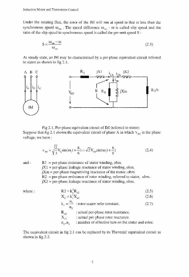
At steady state, an IM may be characterised by a per-phase equivalent circuit referred to stator as shown in fig 2.1.
A B C
Fig 2.1, Per-phase equivalent circuit of IM (referred to stator) Suppose that fig 2.1 shown the equivalent circuit of phase A in which v Ao is the phase voltage, we have :
and:
where:
R1 = per-phase resistance of stator winding, ohm. jXl =per-phase leakage reactance of stator winding, ohm. jXm =per-phase magnetising reactance of the motor, ohm. R2 =per-phase resistance of rotor winding, referred to stator, jX2 = per-phase leakage reactance of stator winding, ohm.
R2 = k;R.2
X2 = k;x.2
k --E.!_ f r : rotor-stator re er constant. n2
R.2 : actual per-phase rotor resistance. xa2 : actual per=phase rotor reactance.
(2.4)
ohm.
(2.5)
(2.6)
(2.7)
n1, n2 : number of effective turn on the stator and rotor.
The equivalent circuit in fig 2.1 can be replaced by its Thevenin' equivalent circuit as shown in fig 2.2.
7
Induction Motor and Trans vector Control
E
! Fig 2.2, Per-phase Thevenin's equivalent circuit of IM
where:
<P 1t - (XI + xm ) =--tan
tA 2 R I
and RO is neglected.
(2.8)
(2.9)
(2.10)
(2.11)
From the per-phase Thevenin's equivalent circuit, the following equations can be derived [1, p.207] :
- The speed-torque characteristic equation of IM :
(2.12)
T = motor output torque.
-Critical motor speed and torque :
(2.13)
(2.14)
-Motor losses :
8
Induction Motor and Transvector Control
T= Pm =~=-3_r;R2 (J) (J) ms (J) ms S
1-s Pm = output power = 3I;R2 (--)
s
Pg = air-gap power = 3I; R2
s
(2.15)
(2.16)
(2.17)
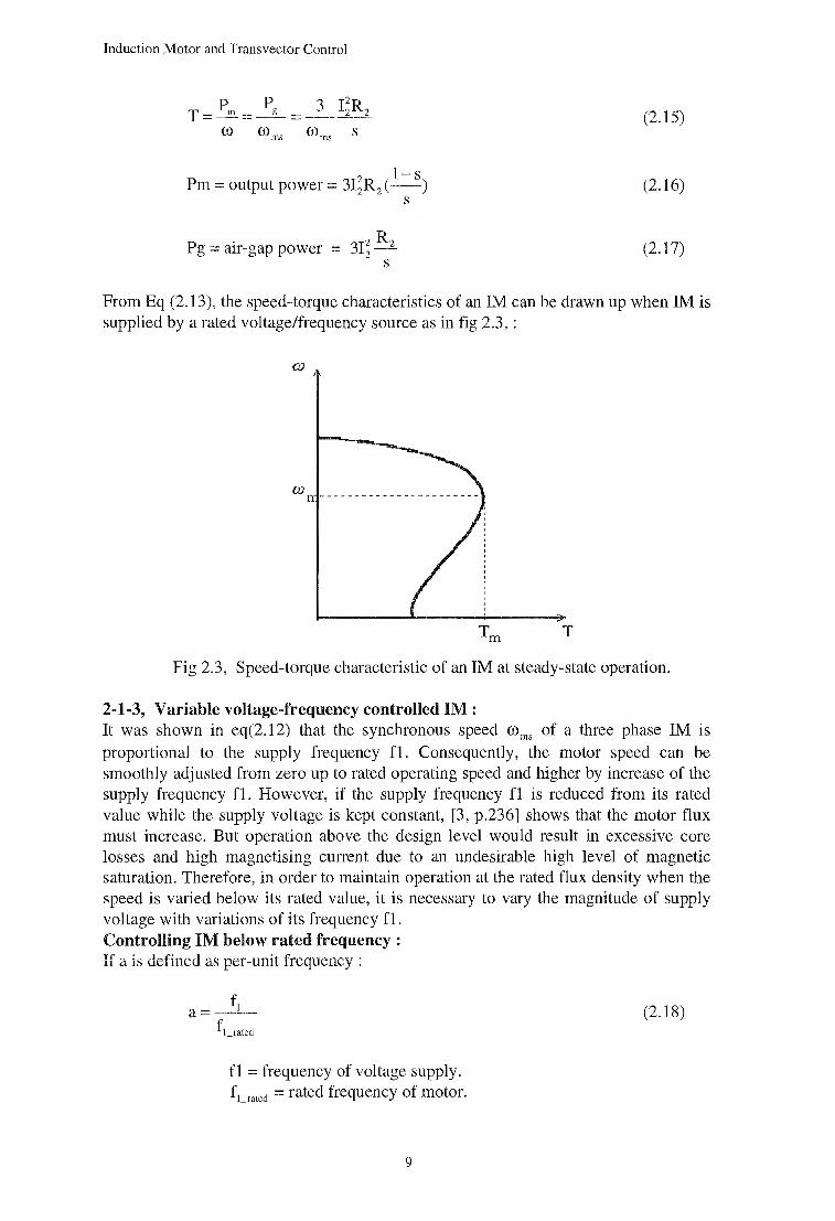
From Eq (2.13), the speed-torque characteristics of an IM can be drawn up when 1M is supplied by a rated voltage/frequency source as in fig 2.3, :
OJ
OJ
Fig 2.3, Speed-torque characteristic of an IM at steady-state operation.
2-1-3, Variable voltage-frequency controlled IM: It was shown in eq(2.12) that the synchronous speed (J)ms of a three phase 1M is proportional to the supply frequency fl. Consequently, the motor speed can be smoothly adjusted from zero up to rated operating speed and higher by increase of the supply frequency fl. However, if the supply frequency f1 is reduced from its rated value while the supply voltage is kept constant, [3, p.236] shows that the motor flux must increase. But operation above the design level would result in excessive core losses and high magnetising current due to an undesirable high level of magnetic saturation. Therefore, in order to maintain operation at the rated flux density when the speed is varied below its rated value, it is necessary to vary the magnitude of supply voltage with variations of its frequency fl. Controlling IM below rated frequency : If a is defined as per-unit frequency :
f a=--~-
fl_rated
f1 = frequency of voltage supply. f1_ratect = rated frequency of motor.
9
(2.18)

Induction Motor and Transvector Control
it will be less than unit (a<l) when frequency of the voltage supply is smaller than rated frequency of motor (f1 < f1_ratect ).
In order to maintain rated motor flux, the e.m.f E must be varied proportionally to frequency fl [3, p.394] :
E - = k = constant fl
The speed -torque characteristic of IM in this case is derived as following : The reactance of motor can be expressed in general form
Hence: E = aEratect
From the per-phase equivalent circuit of fig 2.1, the rotor current is :
where: a(J)ms- (J)
as=--""'---a(J)ms
The speed-torque characteristic is now obtained from (2.15) and (2.20) :
T = _3_ E~atectR2 I as mms (R2 I as) 2 + x;
R Therefore: s = +-2-
m - aX2
T =+-3_E~ated 111 -2wms x2
(219)
(2.20)
(2.21)
(2.22)
(2.23)
(2.24)
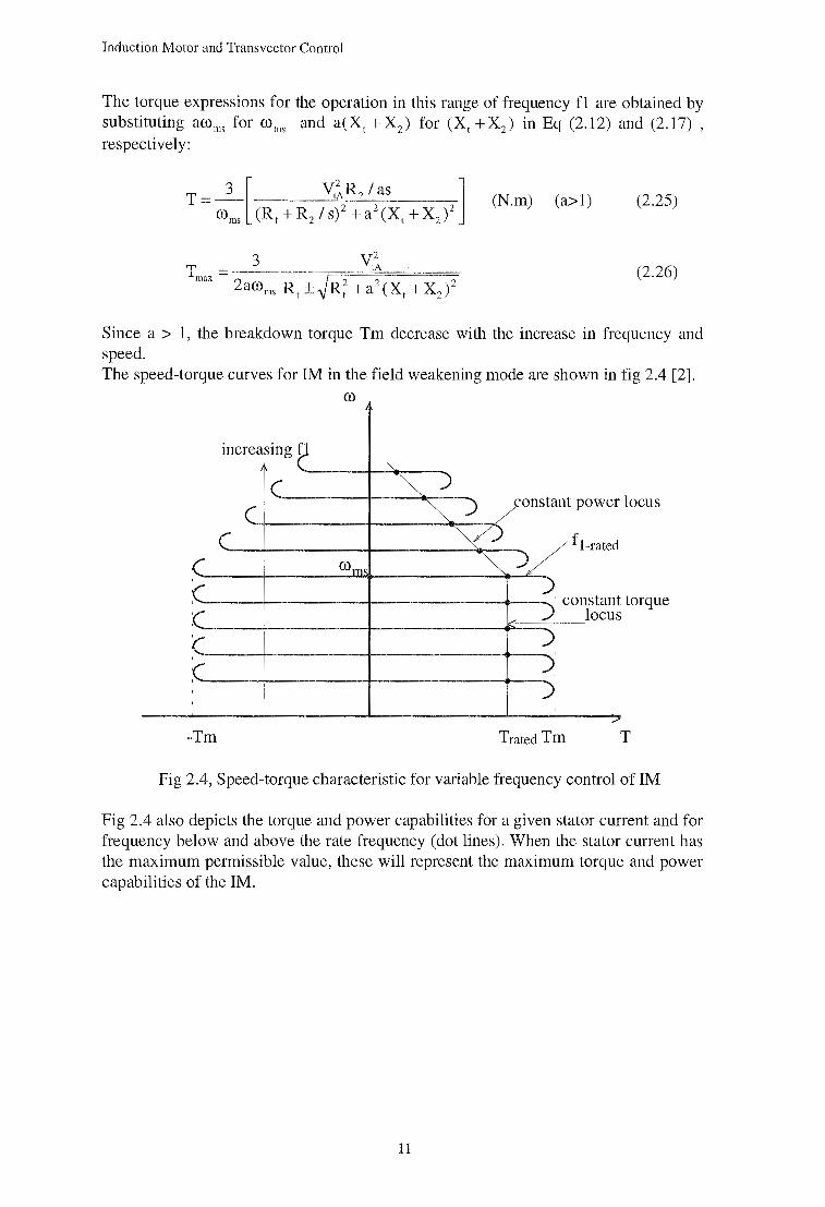
It can be seen that breakdown the torque Tm is constant because both mms and X2 vary proportionally to frequency fl. The speed-torque characteristic of IM when frequency f1 is changed and the motor flux is kept constant is shown in fig 2.4. Controlling IM above the rated frequency : The operation at a frequency higher than the rated frequency takes place at a constant terminal voltage because of the limitation imposed by the voltage supply. Since the terminal voltage is maintained constant, the flux decreases in the inverse ratio of pu frequency a. The motor, therefore, operates in the field weakening mode.
10
Induction Motor and Transvector Control
The torque expressions for the operation in this range of frequency f1 are obtained by substituting amms for ffims and a(Xt +X2 ) for (Xt +X2 ) in Eq (2.12) and (2.17) , respectively:
(N.m) (a>l) (2.25)
(2.26)
Since a > 1, the breakdown torque Tm decrease with the increase in frequency and speed. The speed-torque curves for IM in the field weakening mode are shown in fig 2.4 [2].
(J)
increasing e "
( -~)
c ~ yonstant power
( ~~ J/ft-mtod ( (J)ms
locus
:c ~ constant :c locus
torque
'\. )
·c ~ J:
' /
-Tm Trated Tm T
Fig 2.4, Speed-torque characteristic for variable frequency control of IM
Fig 2.4 also depicts the torque and power capabilities for a given stator current and for frequency below and above the rate frequency (dot lines). When the stator current has the maximum permissible value, these will represent the maximum torque and power capabilities of the IM.
11
Induction Motor and Transvector Control
2-2, Transvector control Many different control techniques for controlling an IM has been popular used for a long time [5] : the constant voltage/frequency control, the constant voltage/frequency control with slip regulation, independent torque and air gap flux control (bang bang control, etc. These methods can be classified in to a group called voltage/frequency control that is simple and economical but can be only used for low-performance applications. In industry application, a high-performance drive system is highly awaited. In this regard, the transvector control technique for the IM is used. This chapter will analyse the basic control concepts of the transvector technique, then describes its application in PWM-IM drive system.
2-2-1, Transvector control technique. To analyse transvector control, the operation of IM is considered in the reference frame rotating synchronously with the synchronous electric speed [6] . By such a way, the air gap flux in an 1M can be considered as the flux vector \f' rotating with synchronous speed ffit. Next, the flux vector \f' is considered as an interaction of
- -stator and rotor voltages and currents Ut, it and h. By this discussion, the balance voltage equations of IM in the reference frame rotating at constant speed ffit are :
where:
-vt = Rti1 +p\f't + jcot \f',.
-0= R2h +p\f'2 + j(cot -ffi)\f'2
- -\f't = Lti' +Mh
- -\f'2 = L2 h +Mit
- -*
p is derivative operator. co is motor speed. \f',, \f' 2 are stator and rotor flux. L 1, L2 are stator and rotor leakage inductances. M is the mutual ( or magnetising) inductance :
M=~L 2 m
All the rotor quantities are referred to stator.
(2.27)
(2.28)
(2.29)
(2.30)
(2.31)
If a coordinate system with d and q axis is fixed in the rotating reference frame, a - -
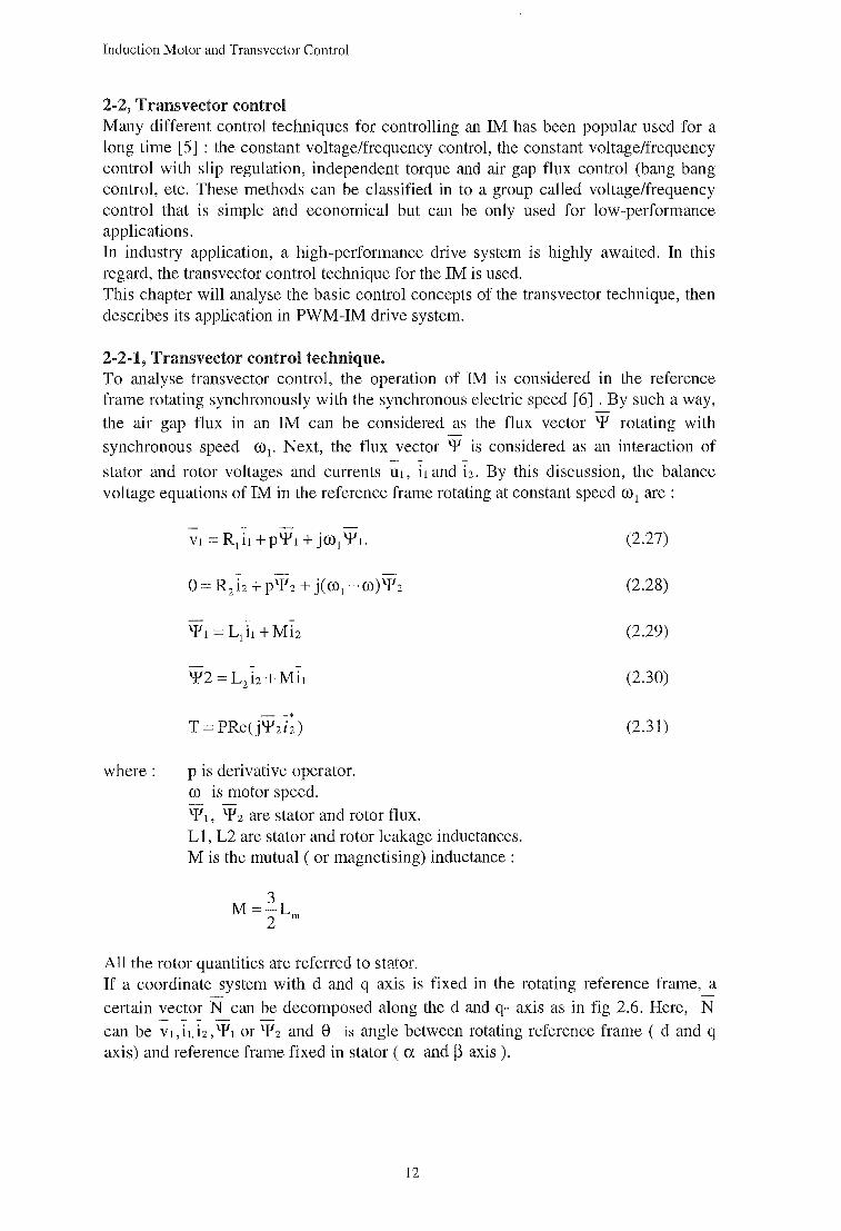
certain vector N can be decomposed along the d and q- axis as in fig 2.6. Here, N can be Vt, i,, b, \f'1 or \f'2 and 8 is angle between rotating reference frame ( d and q axis) and reference frame fixed in stator ( a and~ axis).
12
Induction Motor and Transvector Control
j3
d Rotating at speecto 1
a Fig 2.6, Decomposed vector N along d and q axis
Decompose equation system (2.27) through (2.32) along d and q axis, gives :
vlct = Rlilct +p'I'Ict -mi'I'Iq
v lq = Rl ilq + P 'I'Iq + ffil 'I'Ict
0 = R2i2ct + p'¥2ct - ( ffi1 - ffi) 'P2q
0 = R2i2q + p'¥2q + ( ffil - ffi) 'P2d
(2.32)
(2.33)
(2.34)
(2.35)
and 'P1ct = L1i1ct + Mi2ct (2.35) 'P1q = L1i1q + Mi2q (2.36)
'P2ct = L2i2ct + Milct (2.37) 'P2q = L2i2q + Mi1q (2.38)
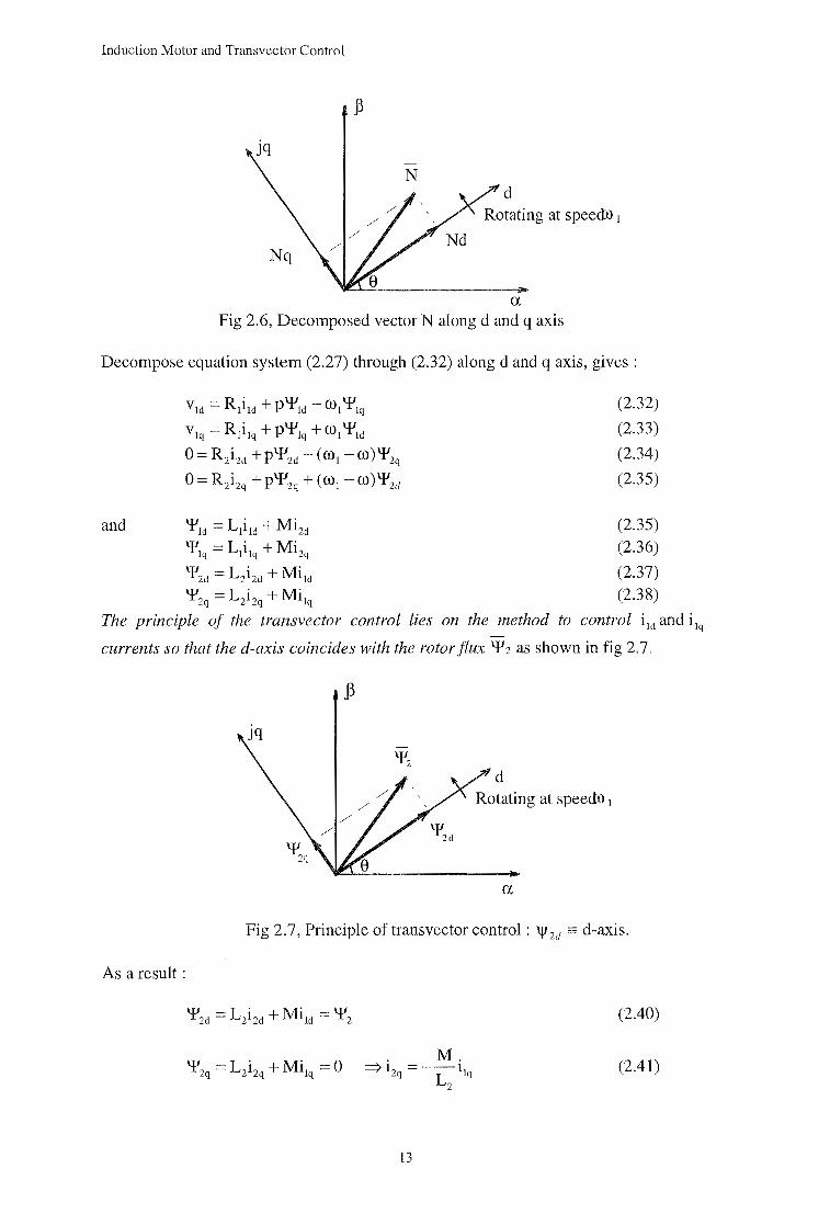
The principle of the transvector control lies on the method to control i1ct and i1q
currents so that the d-axis coincides with the rotor flux '1'2 as shown in fig 2.7.
j3
d Rotating at speecto 1
a
Fig 2. 7, Principle of trans vector control : \jf 2d = d-axis.
As a result:
(2.40)
(2.41)
13
Induction Motor and Transvector Control
and: d\f'2q --=0
dt
From (2.41) and (2.37):
. 1 \TI => 12ct = --pr2
R2 Inserting (2.44) into (2.40), gives :
or
Also, from (2.30) and (2.41):
(2.42)
(2.43)
(2.44)
(2.45)
(2.46)
Equations (2.45) and (2.46) express the fundamentals of the transvector control technique: * The rotor flux transients are determined only by the stator current i1ct along the same d-axis, and the transients decay with the rotor time constant T2=L2/R2. Hence, in context of transvector control, i1ct is called magnetising current. * The expression for the torque is similar to that of a separately exited de motor, ie it can be controlled by controlling independently rotor flux \f/2 and current i1q . Hence,
the stator current component i1q is called the torque current in the present context.
* If the rotor flux \f/2 is kept constant, it follows from (2.45) that for p\f/2 = 0,
(2.47)
Equation (2.47) implies that there is no rotor transients and thus the torque current command is instantaneously translated as a torque command. Thus, an ideal response is obtained. * The transvector can be expanded into the field weakening mode in which the motor speed is higher than rated the motor speed, the voltage at the inverter input is kept constant and the rotor flux is decreased. It can be seen that for transvector control, decreasing the magnetising current i1ct , at a constant voltage input, leads to a higher stator frequency co1 . For a constant torque current, per-unit speed S must be constant, thus higher speeds are obtained : co= co 1 (1- S). Since the torque is given by (2.46), lowering the magnetising current i1ct and keeping the torque current i1q constant will result in reduction in the torque, and hence in
14
Induction Motor and Transvector Control
slower speed response. An increasing in the torque to obtain a higher torque 1s possible by increasing S up to the limit imposed on the total stator current :
I
.
1
2 c· 2 . 2) 11 = 3 lid + llq
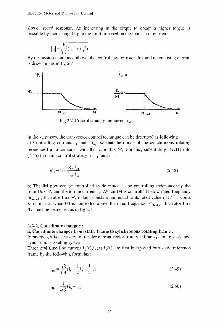
By discussion mentioned above, the control law for rotor flux and magnetising current is drawn up as in fig 2.7
CO rated co CO rated co
Fig 2. 7, Control strategy for current i Ict
In the summary, the transvector control technique can be described as following : a) Controlling currents i1d and i1q so that the d-axis of the synchronous rotating
reference frame coincides with the rotor flux '¥2 . For this, substituting (2.41) into ( 1.45) to obtain control strategy for i1q and i1d :
(2.48)
b) The IM now can be controlled as de motor, ie by controlling independently the rotor flux '¥2 and the torque current i 1ct .When 1M is controlled below rated frequency C0 1_rated , the rotor flux '¥2 is kept constant and equal to its rated value ( E I f = const ).In contrast, when IM is controlled above the rated frequency col-rated , the rotor flux '¥2 must be decreased as in fig 2.7.
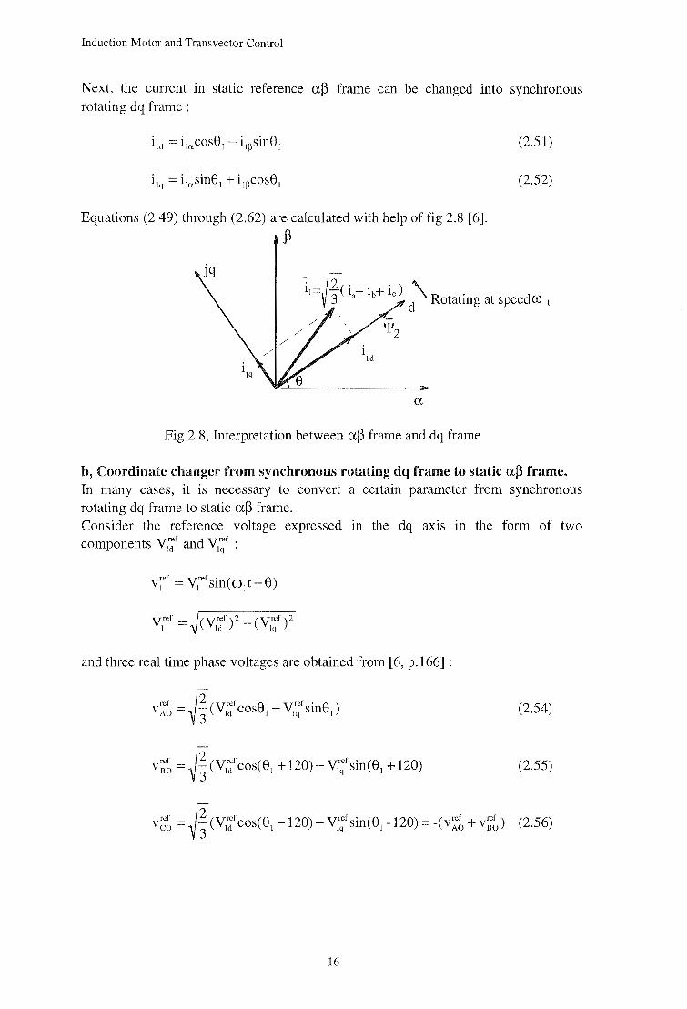
2-2-2, Coordinate changer: a, Coordinate changer from static frame to synchronous rotating frame : In practice, it is necessary to transfer current vector from real time system to static and synchronous rotating system. Three real time line current ia(t),ib(t),ic(t) are first interpreted into static reference frame by the following formulas :
(2.49)
(2.50)
15
Induction Motor and Transvector Control
Next, the current in static reference a~ frame can be changed into synchronous rotating dq frame:
(2.51)
(2.52)
Equations (2.49) through (2.62) are calculated with help of fig 2.8 [6]. j3
-1. 2c·. ') J-
1== - 1 + 1 + 1c . 3 a b d'\ Rotatmg at speedco I
1 !d
a
Fig 2.8, Interpretation between a~ frame and dq frame
b, Coordinate changer from synchronous rotating dq frame to static a~ frame. In many cases, it is necessary to convert a certain parameter from synchronous rotating dq frame to static a~ frame. Consider the reference voltage expressed in the dq axis in the form of two
V ref d yref , components Ict an lq •
vref == yref sin(co t + 8) 1 I 1
and three real time phase voltages are obtained from [6, p.166] :
ref f2cvref 8 yref . 8 ) V AO = ~ 3 ld COS I - lq Slil l (2.54)
(2.55)
vref = ficvrefcos(8 -120)- yref sin(8 -120)- -(vref + vref) (2.56) CO ~ 3 ld 1 lq 1 - AO BO
16
Induction Motor and Transvector Control
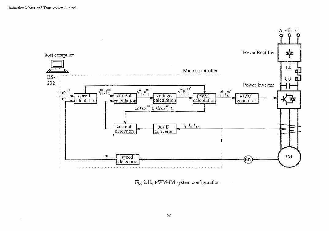
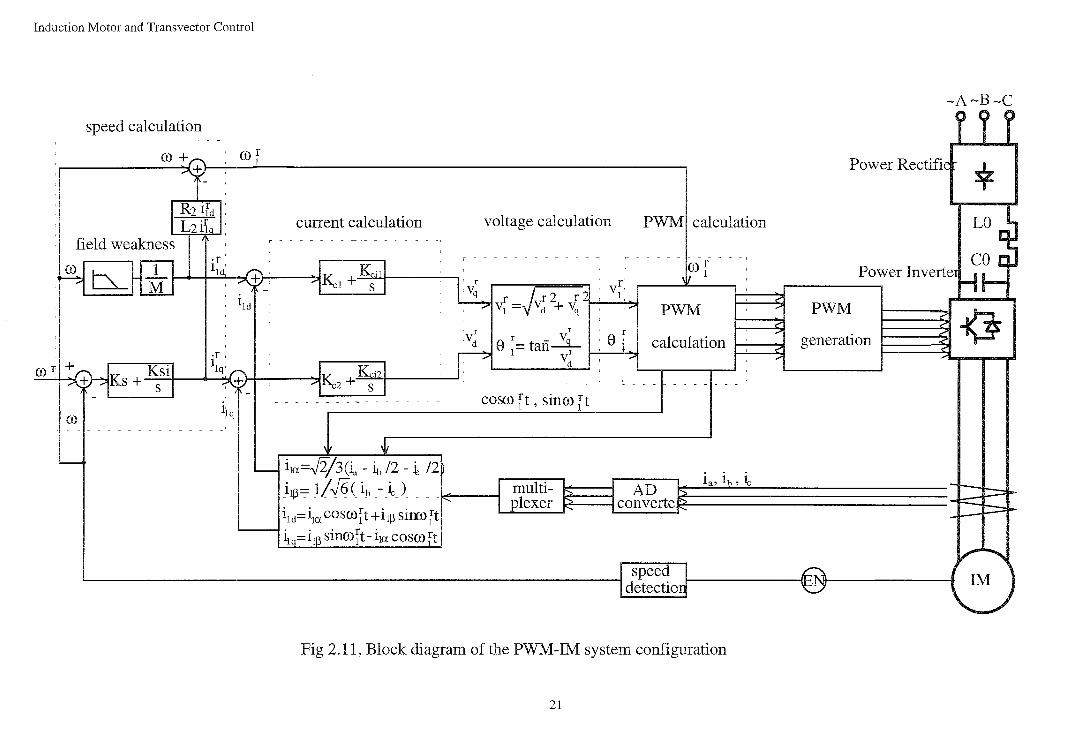
2~2-3, PWM-IM transvector control drive system : The PWM and transvector control technique can be combined to produce a high quality PWM-IM drive system. Concerning flux vector detection, the direct sensing method of the air gap flux by the use of Hall probes is most desirable in theory. From the viewpoint of practical application, this method suffers from high cost and unreliability of the measurement. From this regard, the indirect sensing methods of the rotor flux vector has been developed, which can be divided into two groups. In the first group, the rotor flux vector is obtained by integrating the induced voltage detected directly via sensing coils or calculated indirectly from the stator current and voltage. This method suffers from the inaccuracy of the flux estimation in the low speed region arising from the inaccuracy of the integration. In the second group, the rotor flux vector is estimated from stator currents and rotor speed on the basis of the rotor circuit equations of an IM in the synchronously rotating reference frame with rotor flux vector. Since this method does not require any integration, the rotor flux vector can be estimated even in the standstill. The major weakness of this method is the sensitivity of the estimation to change of rotor parameters, such as rotor resistor, arising from a magnetic saturation and a change of temperature. On the other hand, in order to realise the high response of current control (to ensure the actual stator current must be adjusted instantaneously and precisely according to their reference current. A fast switching PWM inverter with a local feed back loop is usually utilised for the approximate current control and is sufficient for many industrial applications. However, the high gain current controller is generally required to compensate for the induced voltage. Otherwise, the amplitude and phase error between the actual stator current and its reference become no longer negligible, especially in the high speed region, which deteriorates the vector performance. On the contrary, the high gain current loop produces high acoustic noise, unless the switching frequency of the PWM inverter is extremely high (over 20 kHz). To overcome this problem, another type of current control has been developed in which the stator current are transformed into two de components, that are, a magnetising current component and a torque current component, and then these two de components are controlled, respective to transvector control law. This section describes a microprocessor based high performance transvector control system in which the indirect rotor flux estimation method and the de current component method are employed. Fig 2.10, and 2.11, show the configuration of the PWM-IM transvector control system. It can be seen that the system is composed of a current and speed detection, a speed controller, two current controllers, a PMW calculation, a PWM generation, and a transistor inverter. Here, the main parts of system are discussed.
* Current detection block receives and decomposed three real time line current
current i1ct (Eq(2.48) to (2.50)). These current components must be controlled independently by the transvector control algorithm. * Speed control block gets the reference speed coref from host computer and actual speed co from speed detection. Its output is the reference torque current i~~f .
* Non-linear flux block is used to control magnetising reference current i~~. (fig 2.7). If the actual speed co is below the rated motor speed co-rated, i~~f is kept constant in
17
Induction Motor and Transvector Control
order to keep rotor flux o/2 constant. When the motor speed ro increases beyond corated, i~~f must be reduced. * Rotor flux position block controls position of the rotor flux '¥2 to ensure transvector control algorithm : rotor flux must coincide with d-axis of synchronous rotating frame. From (2.48) :
(2.57)
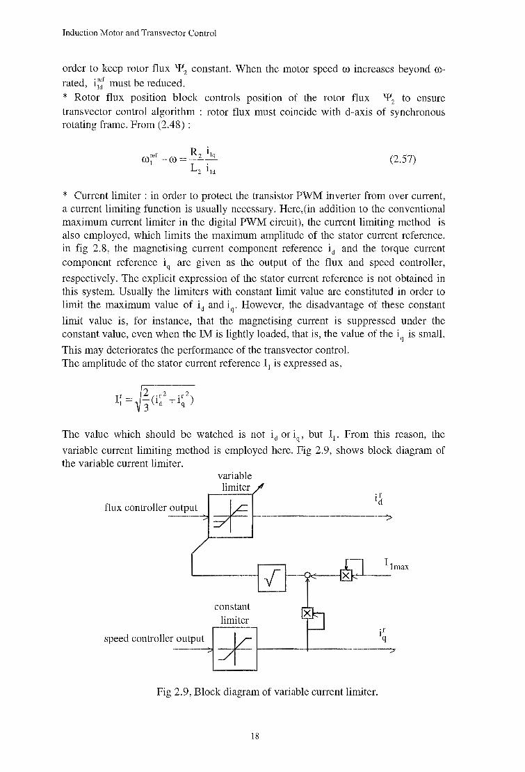
* Current limiter : in order to protect the transistor PWM inverter from over current, a current limiting function is usually necessary. Here,(in addition to the conventional maximum current limiter in the digital PWM circuit), the current limiting method is also employed, which limits the maximum amplitude of the stator current reference. in fig 2.8, the magnetising current component reference id and the torque current component reference iq are given as the output of the flux and speed controller,
respectively. The explicit expression of the stator current reference is not obtained in this system. Usually the limiters with constant limit value are constituted in order to limit the maximum value of id and iq. However, the disadvantage of these constant
limit value is, for instance, that the magnetising current is suppressed under the constant value, even when the IM is lightly loaded, that is, the value of the iq is small.
This may deteriorates the performance of the transvector control. The amplitude of the stator current reference I1 is expressed as,
The value which should be watched is not id or iq, but I1• From this reason, the
variable current limiting method is employed here. Fig 2.9, shows block diagram of the variable current limiter.
flux controller output
variable limiter
constant limiter
11max
speed controller output ____IL ~ 711-----+---
Fig 2.9, Block diagram of variable current limiter.
18

Induction Motor and Transvector Control
This limiter enables the system to control i~d in response to i;·q in order to limit the
stator current reference so that it does not exceed the preset maximum value I1_max . It is of course necessary to put the minimum value in the variable limiter of i;·ct . * Two current controller - the magnetising current component controller and torque current component controller- are used to achieve a good performance of system in both steady state and transient operation. Since the quantities to be adjusted by these controllers are de quantities, conventional PI control technique can be successfully employed. * Two reference voltage from current controllers are sent to PWM calculation block where time delay and pulse width time PWM signal are determined. * Depending on the time delay and pulse width time calculated from the PWM calculation block, the PWM generation block produces PWM signals. Then, PWM signals are amplified and sent to the base gates of power transistor of inverter.
In conclusion, this chapter overviews the steady-state characteristics of an IM as well as the basic concepts of the transvector control. It shows that if the stator voltage and current of an IM are converted from stationary reference frame to the synchronously rotating reference frame, the IM will behave like a separately exited de motor, ie motor flux and torque can be controlled independently. Therefore, the high dynamic performance of the IM drive system can be achieved with the transvector control technique.
19
Induction Motor and Transvector Control
host computer
RS-232
co
AID converter
Micro-controller
~ ,lb ,lc.
Fig 2.10, PWM-IM system configuration
20
~A ~B ~C
Power Rectifier * Power Inverter
~
Induction Motor and Transvector Control
-A-B-C
speed calculation ill r ~ - - - - - - - -
CO+
,~b._ ·f,
~ I J l11d
cor 1
current calculation voltage calculation PWMI calculation
cor II 1
Power Rectific
* ~:~ Power Invert~b I
I ~....---------,1
~ PWM PWM ?
t .,...,
CO rl ~+ ·f I ~ . , ,Vd r Vr
Ks + Kstl J \~ 1 . . e r= taii~q s , + ~ K,;,l · · v' ' z+~ , , ct . - s r · r COS(!) 1 t , Slll(l)
1 t
generation I ~ ~ I ' ' &
.... 8·
-' -~--calculation I ~
(!) l~q
w _j_ '---
'--I in~/3(~ - ib /2 - i /2~ . ~ i, ib, t :t:::t=f-iJ!l= 1/J6 ( ;• -. U r I ;J~~~r ~ I co;{ferte :r:=t=t-I1ct= 11a COS(!) 1 t + 1113 SlliD 1 t
, 1. . · r · rt 119= 11p smco 1 t-In cosco
1
~------------·----------------------------------_J~d~~~~oJ ~ ~
Fig 2.11, Block diagram of the PWM-IM system configuration
21
Dynamic ofPMW-IM Drive System
Chapter 3: Dynamics of PWM-IM drive system.
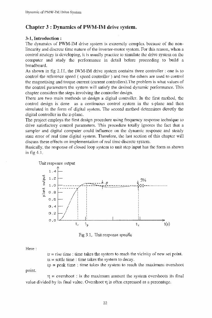
3-1, Introduction : The dynamics of PWM-IM drive system is extremely complex because of the nonlinearity and discrete time nature of the inverter-motor system. For this reason, when a control strategy is developing, it is usually practice to simulate the drive system on the computer and study the performance in detail before proceeding to build a breadboard. As shown in fig 2.11, the IWM-IM drive system contains three controller : one is to control the reference speed ( speed controller ) and two the others are used to control the magnetising and torque current (current controllers).The problem is what values of the control parameters the system will satisfy the desired dynamic performance. This chapter considers the steps involving the controller design. There are two main methods to design a digital controller. In the first method, the control design is done as a continuous control system in the s-plane and then simulated in the form of digital system. The second method determines directly the digital controller in the z-plane. The project employs the first design procedure using frequency response technique to drive satisfactory control parameters. This procedure totally ignores the fact that a sampler and digital computer could influence on the dynamic response and steady state error of real time digital system. Therefore, the last section of this chapter will discuss these effects on implementation of real time discrete system. Basically, the response of closed loop system to unit step input has the form as shown in fig 4.1.
Here:
point.
Unit response output
-1-' ::::1 CL ....., ::::1 Co
-1-' c <:l
CL
1.4
1.2
1.0
0.8
0.6
0.4
0.2
0.0 t(s)
Fig 3. 1, Unit response specific
tr = rise time : time takes the system to reach the vicinity of new set point. ts = settle time : time takes the system to decay. tp = peak time : time takes the system to reach the maximum overshoot
11 = overshoot : is the maximum amount the system overshoots its final value divided by its final value. Overshoot 11 is often expressed as a percentage.
22
Dynamic ofPMW-IM Drive System
Normally, these requirements are given by customer. In this project, these specifications are supposed as :
+ tr <= 0.2 s + ts <= 0.5 s + 11 <=10%.
3-2, Mathematic model of the PWM-IM drive system.
The first step in control design is to model the overall system. Depending in the actual system, a system can be modelled in the form of mathematical equation, state variable, block diagram , state space or their combination. In this project, the mathematical equation and block diagram method are combined to model the PWM_IM vector control system.
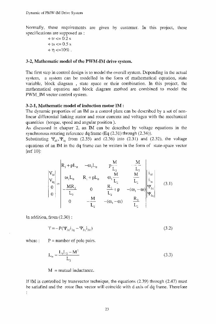
3-2-1, Mathematic model of induction motor IM: The dynamic properties of an 1M as a control plant can be described by a set of nonlinear differential linking stator and rotor currents and voltages with the mechanical quantities (torque, speed and angular position ). As discussed in chapter 2, an 1M can be described by voltage equations in the synchronous rotating reference dq frame (Eq (2.31) through (2.34)). Substituting \f1cl' \f1q from (2.35) and (2.36) into (2.31) and (2.32), the voltage
equations of an IM in the dq frame can be written in the form of state-space vector [ref 10]:
-rolLa M M
Rl +pLa p-L2 L2
vld M M 1lct rolLa Rl +pLa ro-
vlq JL L2 llq 2 0 _MR2 R \}'2d 0 _2+p -( rol - ro) 0 L2 L2 \}'2q
0 M
-( rol - ro) R2
L2 L2
(3.1)
In addition, from (2.30) :
T =-P(\f2cti2q - \f2qi2ct) (3.2)
where: P = number of pole pairs.
(3.3)
M =mutual inductance.
If IM is controlled by transvector technique, the equations (2.39) through (2.47) must be satisfied and the rotor flux vector will coincide with d axis of dq frame. Therefore
23
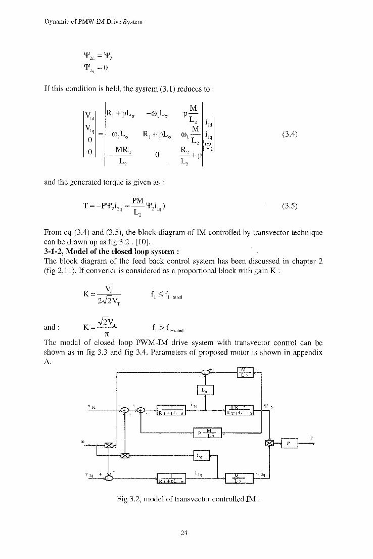
Dynamic ofPMW-IM Drive System
If this condition is held, the system (3 .1) reduces to :
vld Rl +pLa -coiLa
vlq = coiLa Rl +pLa
0 (3.4)
0 _MR2 0 L2
and the generated torque is given as :
(3.5)
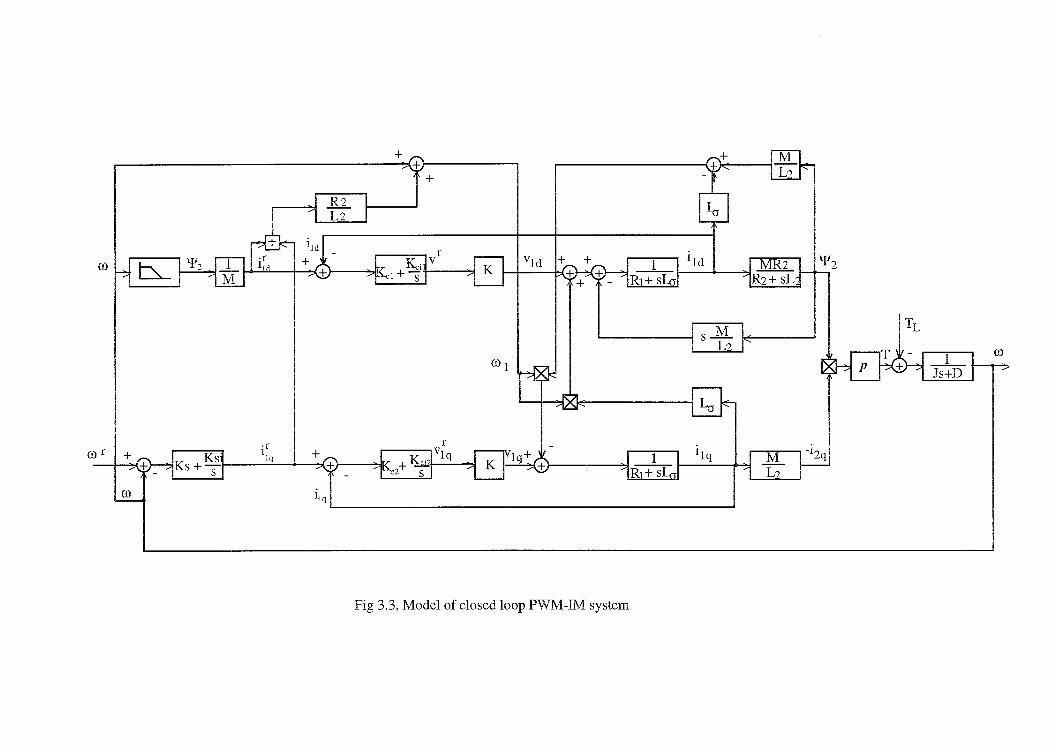
From eq (3.4) and (3.5), the block diagram of 1M controlled by transvector technique can be drawn up as fig 3.2 . [10]. 3-1-2, Model of the closed loop system: The block diagram of the feed back control system has been discussed in chapter 2 (fig 2.11). If converter is considered as a proportional block with gain K:
and: K= Jivd TC
The model of closed loop PWM-IM drive system with transvector control can be shown as in fig 3.3 and fig 3.4. Parameters of proposed motor is shown in appendix A.
v ld
Ol 1
i lq
Fig 3.2, model of transvector controlled IM.
24
(J)
wr ·[
llq
TL
(J)l
Fig 3.3, Model of closed loop PWM-IM system
Dynamic of PMW-IM Drive System
QProduct
I~ !11t[1jFcn
I
L-EJ Constant
1 .2*1.25S+ 1.
s speed control!
l.~H ~GainS ' Pcod"ct1 ~I
Gain?
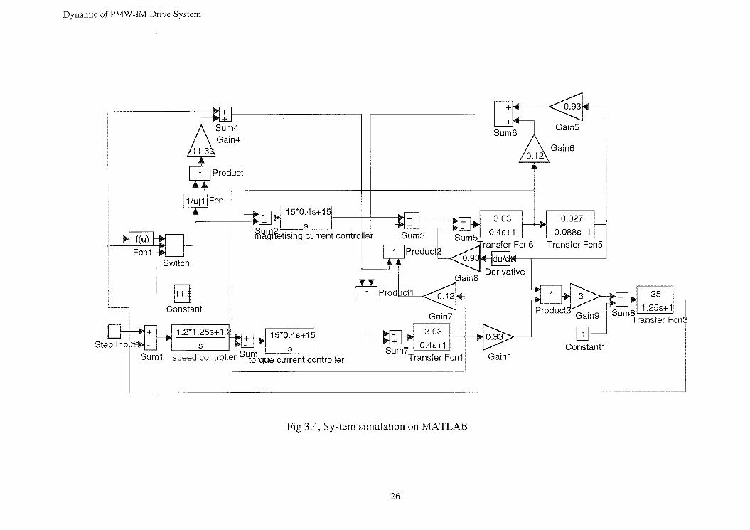
Fig 3.4, System simulation on MATLAB
26
3.03
0.4S+ 1
Gain1
0.027
0.088s+1
Transfer Fcn5
;r~ 25
~n9 I Sums I 1 .25s+ 1 l...!_J-- Transfer Fen
Constant1
Dynamic of the PWM-IM Drive System
3-3, Control design : It can be seen that the transvector controlled PWM-IM system is described by a highorder non-linear multi-variable state-space equation. Therefore, its control and feedback processing is very complicated. To simplify problem, the conventional design method suggest that the system can be linearized on the basis of the small signal perturbation at a particular operating point and then the conventional feedback analytical methods such as the Nyquist and Bode plot technique can be applied. However, if the operating point changes, the poles, zeros and gain of the linearized system will also change, mandating a new set of control parameters for the system. Therefore, the conventional method requires to check and tune control parameters, theoretically, at all operating point of the speed range, then a fixed control structure with a fixed set of control parameters is determined so that the worse-case system performance is acceptable. With the availability of user-friendly simulation software packagess such as SIMNON, ACSL, MATLAB, etc, a new method is suggested to avoid such laborious design technique. It is clear that there is a strong coupling between stator current component and stator voltage component via motion voltage. In order to decouple the motional voltage in the reference voltage, in the proposed method, the motion induced coupling voltages are considered as disturbances to reference voltage. By such a way, two current loops become independent and can be synthesised as linear loops with conventional linear feedback analytical methods. The synthesis of the speed loop is more complicated due to non-linearity of the system and needs helps of computer. It first is designed by hand, ignores the effects of the rotor flux and then the system is simulated by simulink tool of MATLAB software package to check and tune the parameters of the controllers at all the most important points of the speed region until specified requirements of the system are met.
3-3-1, Overview of control design : There are many methods that can be used to design a controller such as root locus, frequency response, pole-zero placement, state-space, etc. In this project, the frequency response method is chosen to design the current controllers. The principle of the frequency response method is outlined as follows : In terms of the frequency response, the transfer function of a system can be expressed by a magnitude I H( (J)) I and a phase I <p( (J)) I curve respect to frequency (J). These curves are introduced by Bode (1960). By using Bode plot, the stability and dynamic response of system can be entirely analysed through some important factors related to Bode plot diagram. They are : + Gain margin GM : is defined as the difference between 1 and I H( (J)) I curve at which the gain of the system is less than the neutral stability value ( phase curve crosses 180°.) + Phase margin PM : is the difference between I <p( (J)) I curve and -180° when magnitude curve crosses 1. The stability and dynamic response of the system now can be stated as :
* The system is stable when I GM 1>=1 or PM >=0. * Damping of the system decreases when PM increases.
28
Dynamic of the PWM-IM Drive System
In order to apply the Bode plot diagram technique to design a controller, a dummy function must be introduced depending on the required specifications. If second order could satisfy requirements, the dummy function will has the form :
(3.6)
The formulas related to parameters of the second order dummy function and system specifications are [ 14] :
(3.7)
(3.8)
where:
~ = damping ratio : (3.9)
ffi11
= undamped natural frequency (3.10)
After the dummy function is determined, the parameter of the controller is somehow calculated so that its Bode plot of the closed loop system is closed to the Bode plot of the dummy function in the range ( + 15 dB,- 15 dB) 3-3-2, Torque current loop : In the case of the current loop, the overshoot is permitted up to 25% while the fast response is necessary. Suppose that 11 = 20% and tp = 0.1s are required, the dummy function of torque current loop is derived from (3.6) through (3.10) (appendix B):
30 Hct(s)=----
s(0.0167s+ 1) (3.11)
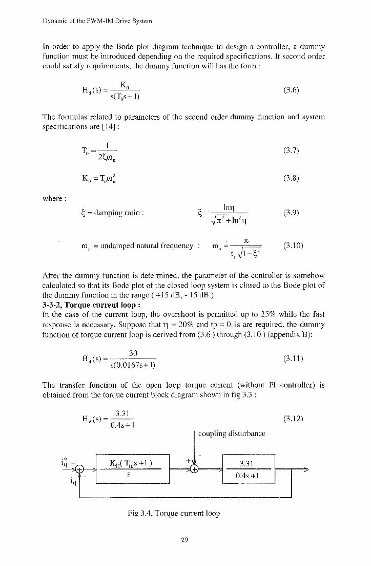
The transfer function of the open loop torque current (without PI controller) is obtained from the torque current block diagram shown in fig 3.3 :
H (s) = 3.31 ct 0.4s+ 1
(3.12)
I coupling disturbance
-·* KtcC Ttcs + 1 ) +\ ~ 3.31
.... s .... + .... 0.4s +1
.... -
lq
Fig 3.4, Torque current loop
29
Dynamic of the PWM-IM Drive System
v~-- 0 ...-. 1 f'L 11'1:::1
PlOO .0 : ;:: :>-<~~~~Jlli~t~~: :::::;::::;::: ............... , ... tk~ freq~~y: .. : ~ ·~
,_ lllO.Q . ....,.,_··~- . . .. .... ...... , ...
' .. . . -·· ·-· ··-. ··-····· ...... :·"-...·····-····---- ·-· ·······-
ltl. tJ : ;:: y~~~~~::::: :~:::1::: i·~>r-~<i:~~ :;: ::;:>; ........ , .. , .,., ············ _,
· ·1· · · · · -~ !~~:~-L 11··-~~~~:. · · ~ · · ~ ·1 L.or-~~~~:-::~::-::_-::-:~:::~·::-::-:~::~:[~:1-::=::~r~::~-:~}~~~~~~~~~~K~l.-,-::-::-::-::~::~::~:::
(r . - '-:--'---'-----L-'----'-----'----'-----'--'-' -::'-::-.L...L'--'---'--l.:~"'--''-~--'--'-'-' o.o j::.o 1000.)
:ra.-:=~ ... :;;-) PhC't:=;.o=-
~~ .---~~~i·i·"-T~;··i~<:_r· r ·1 ! .... 1 .. ri 1r ·1 "' . . . . . . : -,-~~----- L-_J_ o:p~~ loo:p , ,
; ; ! ·-·-rT·-·~: · · ·:, 0:~ ·,+·-~T~y ~=tio+ ! LitJ
-so -----1 l?r1
l~U . ~"":--... .
-L80~~--~-~-~~~~--~~~--~~~~~~~~~-~-'-~---~~ ::'1r1
! l . . . ..
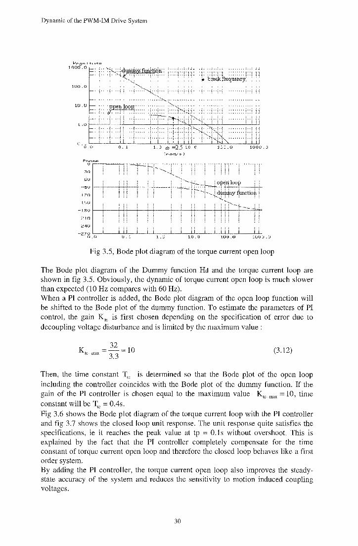
Fig 3.5, Bode plot diagram of the torque current open loop
The Bode plot diagram of the Dummy function Hd and the torque current loop are shown in fig 3.5. Obviously, the dynamic of torque current open loop is much slower than expected (10Hz compares with 60Hz). When a PI controller is added, the Bode plot diagram of the open loop function will be shifted to the Bode plot of the dummy function. To estimate the parameters of PI control, the gain K 1c is first chosen depending on the specification of error due to decoupling voltage disturbance and is limited by the maximum value :
32 Ktc-max =- ""' 10
3.3 (3.12)
Then, the time constant T1c is determined so that the Bode plot of the open loop including the controller coincides with the Bode plot of the dummy function. If the gain of the PI controller is chosen equal to the maximum value Ktc-max = 10, time constant will be Ttc = 0.4s. Fig 3.6 shows the Bode plot diagram of the torque current loop with the PI controller and fig 3.7 shows the closed loop unit response. The unit response quite satisfies the specifications, ie it reaches the peak value at tp = O.ls without overshoot. This is explained by the fact that the PI controller completely compensate for the time constant of torque current open loop and therefore the closed loop behaves like a first order system. By adding the PI controller, the torque current open loop also improves the steadystate accuracy of the system and reduces the sensitivity to motion induced coupling voltages.
30
Dynamic of the PWM-IM Drive System
~ra.:j,.. o:
F'h"'""' ~ -·:····:"":':""''""'' ·:·:" ·: """: 0 • I • ' ' ~ • • • .. ' a I • ' • • ' • • I • • . . . . . . . . . . . . . . . . . . . . . . :: : : : :
:])
. . . . . . . . . . . -6) -·~····~····~·!····· ....... -.:·=·· -.: ... ···! :.: ... .: ... .: .. : ....... : .. .:.
. . . . : : : : : .l<.> ;~ ~ l<.>q..
1?"1
~.......:-..... : 0 ' 0 0 ; : : ~N~~N·~~ : : : : :
. . . . . . . . : . >~. :.'.um.··l)y fiin~~·~ -!5.) _,, .... , .... ,., ............. ,., .. ·: ...... : :.: .. . : . .. : .. :.>.•-, ... : .. : . . .
~ ~ : : : : ~ ~ ~ ~ ~ ~ ~ -~~~--j_ .. : : : :
: : : : : : : :
-20 _,, .... , .... ,., ............. ,., .. ·: ...... : :.: .. . : . .. , .. , ....... , ..
i 1 I i I I I i I i I I i -27) ---L~--~--------~--~--~~~--~~--~~~-W J.: 0.1 L.O ~0 0 ~OC.C 1COC.C.
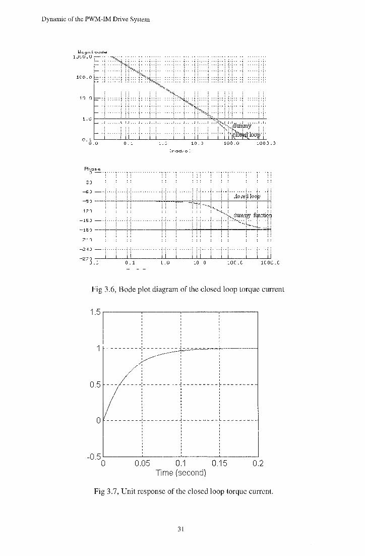
Fig 3.6, Bode plot diagram of the closed loop torque current
1.5 r-----..------.,.-------,.-------,
' ' ' ' . ------- -:-- -J-~.,-~~_:-~---- :···-·····--··-·-·-·-··----
. .,..,"'" ........ ~
/
1
,,./··· ,•' I
/ : 0.5 --- .. "-----:------- ·- --------- --------/ '
/ : /
/ / : :
0 --------~---------~---------L--------0 '
' ' '
-0.5 L...I ___ .,L_ __ ___,l, ___ ___,_ __ ____,
0 0.05 0.1 0. 5 0.2 Time (second)
Fig 3. 7, Unit response of the closed loop torque current.
31
Dynamic of the PWM-IM Drive System
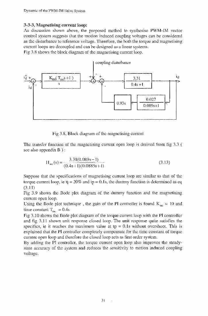
3-3-3, Magnetising current loop: As discussion shown above, the proposed method to synthesise PWM-IM vector control system suggests that the motion induced coupling voltages can be considered as the disturbance to reference voltage. Therefore, the both the torque and magnetising current loops are decoupled and can be designed as a linear systems. Fig 3.8 shows the block diagram of the magnetising current loop.
coupling disturbance
-·*
~ KmJ Tmc" +1) +\ + 3.31 ld + -j;; -- I__.
- s 0.4s + 1 ld -
0.027 0.93s ¢-
0.089s+l ~
Fig 3.8, Block diagram of the magnetising current
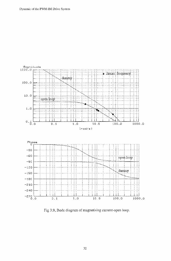
The transfer function of the magnetising current open loop is derived from fig 3.3 ( see also appendix B ) :
Hmc(s)= 3.31(0.089s+1) (0.4s+ 1)(0.0885s+ 1)
(3.13)
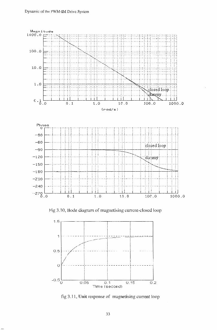
Suppose that the specifications of magnetising current loop are similar to that of the torque current loop, ie 11 = 20% and tp = 0.1s, the dummy function is determined as eq (3 .11) Fig 3.9 shows the Bode plot diagram of the dummy function and the magnetising current open loop. Using the Bode plot technique , the gain of the PI controller is found Kmc = 10 and time constant Tmc = 0.4s Fig 3.10 shows the Bode plot diagram of the torque current loop with the PI controller and fig 3.11 shown unit response closed loop. The unit response quite satisfies the specifics, ie it reaches the maximum value at tp = O.ls without overshoot. This is explained that the PI controller completely compensate for the time constant of torque current open loop and therefore the closed loop acts as first order system. By adding the PI controller, the torque current open loop also improves the steady-state accuracy of the system and reduces the sensitivity to motion induced coupling voltage.
31
Dynamic of the PWM-IM Drive System
1.0~:-:~:-::-::~::~:;-::~::-~;:-::-::~::-::-:~~:-:~:~~:~i:-::-:~~:-::-:~~:~:i~:~~:~, -.:-:~~:~::~---~::~:;-::~::~;:-::-::~::-::-::~::~:~
:;::::: :):::: ;::: :;:::::)s:.-·~<L:::):::: ;:: 0- 1 LO 10.0 100.0 1000.0
(rad/s)
Phase 0 r-----:--'"':""""~-';--'--' :_:_· ·..:__· ·:-::·_:__· : .. : , ..
;~; ; .. ; ; ;; ; ; ; ;; ·~·:··,:· ... :·· ., ··-··.' .... , .. ,., ..... , .... , .... ' .. :: ': -30
-GO ·: ·: ·· · ·- · ·· · ·: ·; ·:- · · ·:· · · ·:·-: · 1 · ofie~·10·~r·: ·:·: . .
-9 0 r--~-~-~-~--~~~""'-'-'-'-'' -~:_:.~-~~~~: .... ~.- ..
=~:: · · ·: 1:: t: j ::::::1::::1 ·:: · 1.: · ·:: 1::::1::::1 t::: r~~~t-~id~~: 1::::1.: :: :::::: :: .. :: :::~~~j
-180 ~----~--~~~------~~--~----~----~--~~----~--~~
-ZlO o o • o .. o o I" o , o 1 o o o • .. ~ o o • .. o • 1 o .. ' I ' 0 0 ' 'I 0 0 0 0 .. 0 0 I ' .. 'I • 0 ' 0 .. 0 0 0 0 .. ' • I ' .. ' I ' 0 0 • .. 0 ' ' ' . . . . . . . . . . . . . . . . -240
. . . ... ·-··-·- ...... --···-. ···- ..... ·-···.- ... ·-··-···-· .. ·-. -··- ..... --···· . . . . . . . . . . . . . . . . . . . . . . . .
0- 1 1.0 10 . 0 100.0 1000.0
Fig 3.9, Bode diagram of magnetising current-open loop.
32
Dynamic of the PWM-IM Drive System
1000.0
100.0
10.0
::;:::-><. __ :;::::::;::::;::::j::::::j::::;:::: • • 'I • • • • .. • • r :U.,'I. • 1 • • o o ~ ~ • • , 'I , o I , 'I • 1 • • • • ., • , o • 'I • • 1 •
: : : :--"-- : ' ' ' ' : . . . . . ........... . . ' ':' • • '~' • ~ '~ •: "'-,,~~:'' • 'I' 'I • 'I' I"' ': •"' 'I'' I •
:: j::::;::;: j :::::: j ::">i~~-: j :j:::: j:::: j:::: ' 'j''' ': '': ': ·: '''' ~-'' ':' ': --->~<' '~'' '' :'': . : : ; ; ; ; ; ; ' ; ; ; ;;: : : ; : ) ; ; : : ; ; ; : ; ; : : : :~'·t<~~; ; : ; . -~ ... -~-·~·~·: ····~~ ... ~. ·:·~·:··· -~"'' ~~~-' ' ~ ' ' ' ' ~ • ' r ' ~ 'I • • • • ~ a ' ' ' , • • I • • ' I ' • • • , • • • ' , • • I •
' . . . . . ' . . . ... .. . ... . ... . .. .. . . ., ........ , . .,., .......... ., .. , . .,., .. . . . . . . . ... ' . . .. '
' ' .
• • ••••at• '1'1''' ... , ''''I ••
. ···:· ·:· :·:··. ·:····: .. . ... ":. ·:· ··:·· .. ":'''' ":''
........ , . .,., .... ., ....... . . ... -.................. . . . . . . . . . . . -: . - : . ~ . : .... ": .... ": ..
. ..... -··- ·····-- .... - ..
.... ., .. , . .,., .... ., .... ., ..
. ...... -.. ., ..... - ., .... ~ .. . . . . . . ' ' . 1.0 ~~---~~~--~---~~~--~-~~~~~~~~~~--~--~~~
::::::::::::::::::::::::::::::::::: :; :::::::::::::::: : ::~~d6~~ai6ci~: . . . .. .. i.- ;·~-~ . y .. ~ ..
Phase Q
-30
-GO
0. 1 LO i 0 '0 100.0 1000.0
Crod/s)
,,., •• '"''r'"' • • • • 'I • • • • 'I • • I • .. • I • • • • 'I • • • • 'I • • I • .. • I u ' ' ' 'I • • • • .. • ~ I ' .. • I • • • • 'I ' ' ' ' 'I • • I • 'I 'o . . . . . . . . . . . . . . . . .... I I I I I I I I I I I I I I I I I I I I I I I I
,,.,,, .,.., r ,,, '''',.,'''I' '1''1'1''' '" '''' ... 'I,,,,.,,,,,'''"' •I• ,,,,,'"'I'''' 'I ''I '"'I . . . . . . . . . . . . . . . . . . . o m o o o • ~ o o n o a o .... -..... -.... -...... -.... -.... -.. - ... -.... ~ . -.. -..... --.... -.... - .. . . ..
: : : · · : : j ~lp~ed lpop j j j j -go r-~--~~~--~---~~~----~~~~~~---~~~--~--~~~
=::: i !ill !:T itT!TIFb~--180
' ~ • • • • ~ ' ' r 0 '1 ° I • • • • 'I • 0 ' ' 'I ' ' I ' .. ' I ' ' ' ' 'I 0 ' 0 ' 'I ' ' I ' • 'I • ' 0 ' 'I ' ' 0 ' 'I ' • I ' 't ' I ' ' ' • .. ' ' ' ' . . . . . . . -Z10 . . . . . . . . . . . . . . .
-240 . . . . . .
..... ·-· ·-·- ...... ·-· .... ···-··· ......... -· .. ·-··-· ··-· ···-·-··- ·····-- ... . . . . . . . . . . . . . . . . . . . . . . . . . . . -270 ~~---L-L~---L--~~~--~--~~~--~~~~~--~~~~
0.0 0 - 1 1.0 i 0 . 0 100.0 1000.0
Fig 3.1 0, Bode diagram of magnetising current-closed loop
1.5.---------.---------.---------.--------.
1 - - - - - - - - -:- - - - - - - - - ~ - - - - - - - - :::: .... ~ ... :: ... :::-... :::-.... ::: .. .:::::-···""'"'"""'"'"' ,,, .. , .. ..-••""........---~ :
~~---~·· : : /, .. ~·: : :
-~--~·"''./ [ : ~ 0 '5 - - -/""- - - - -:- - - - - - - - - ~ - - - - - - -- - :- - - - - - - - -
,/ : : : / : : :
I t : ; : -1
,l : : :
o'---- -- -~- -- ----' ----- -,--- --
-0.5 ~ ' ' ' ~ 0 0.05 0.1 0.15 0.2
Time (second)
fig 3.11, Unit response of magnetising current loop
33
Dynamics of the PWM-IM Drive System
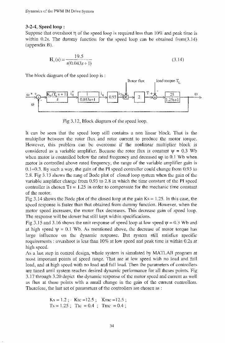
3-2-4, Speed loop : Suppose that overshoot 11 of the speed loop is required less than 10% and peak time is within 0.2s. The dummy function for the speed loop can be obtained from(3.14) (appendix B).
H ( ) 19.5 s s = s(0.043s+ 1)
(3.14)
The block diagram of the speed loop is : Rotor flux load torque TL
Fig 3.12, Block diagram of the speed loop.
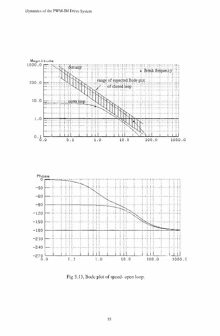
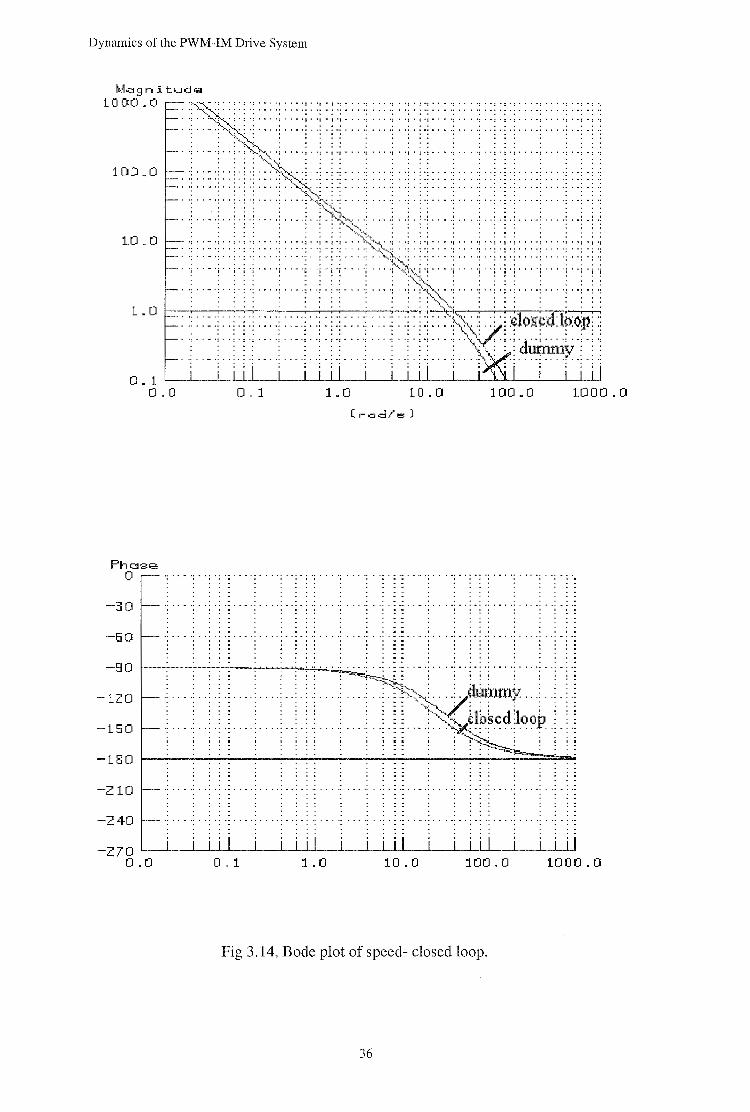
It can be seen that the speed loop still contains a non linear block. That is the multiplier between the rotor flux and rotor current to produce the motor torque. However, this problem can be overcome if the nonlinear multiplier block is considered as a variable amplifier. Because the rotor flux is constant \If = 0.3 Wb when motor is controlled below the rated frequency and deceased up to 0.1 Wb when motor is controlled above rated frequency, the range of the variable amplifier gain is 0.1 +0.3. By such a way, the gain of the PI speed controller could change from 0.93 to 2.8. Fig 3.13 shows the rang of Bode plot of closed loop system when the gain of the variable amplifier change from 0.93 to 2.8 in which the time constant of the PI speed controller is chosen Ts = 1.25 in order to compensate for the mechanic time constant of the motor. Fig 3.14 shows the Bode plot of the closed loop at the gain Ks = 1.25. In this case, the speed response is faster than that obtained from dummy function. However, when the motor speed increases, the motor flux decreases. This decrease gain of speed loop. The response will be slower but still kept within specifications. Fig 3.15 and 3.16 shows the unit response of speed loop at low speed \If= 0.3 Wb and at high speed \If = 0.1 Wb. As mentioned above, the decrease of motor torque has large influence on the dynamic response. But system still satisfies specific requirements : overshoot is less than 10% at low speed and peak time is within 0.2s at high speed. As a last step in control design, whole system is simulated by MATLAB program at most important points of speed range. That are at low speed with no load and full load, and at high speed with no load and full load. Then the parameters of controllers are tuned until system reaches desired dynamic performance for all theses points. Fig 3.17 through 3.20 depict the dynamic response of the motor speed and current as well as flux at these points with a small change in the gain of the current controllers. Therefore, the last set of parameters of the controllers are chosen as :
Ks = 1.2; ~ Ktc =12.5 ; Kmc =12.5; Ts = 1.25 ; Ttc = 0.4 ; Tmc = 0.4 ;
34
Dynamics of the PWM-IM Drive System
~bgn i l:.ud""
1 o a o . o : : r~~-~<,: : ~ : jd~~< : : .. · · : ; : ~ : : : : ; : : : : ; : : ~ : ; : ~ : : : : ; : : : : ~ : ~r~ :fi.*uen;t;y\ :
. . ' 0 • 'l 0 I ' ' 0 0 't 0 ' 0 0 "I • o f • "I 0 I ~ 0 0 0 "I ' o o o "I • w I ' "I • I • • • ~ "f • o • • "f • o I •
100.0 : tano-e of esnec:ted Bode nlot: : : : : :
I 'I 0 I 1 I ,q 'I I I I I 'I I~~ I I 'I II R I I I 'I I I I~~ 'I I 8 I I 'I I I I I I • '1 I I I I • I I I I ... : :7:: : i ?r:qt~~~P~?? i: ::::::::::::::: i:::: :::: : . . . .
0 0'10000 "fOOt >'10fBOOO"f 0 000"fo•o' •• ,. 00N"f0000 .... , 0
0. 1 1.0 i 0 '0 100.0 1000.0
Phe~se 0 r-~.o...:...:.."'-"..:.·..:.,··:..:.··"''''~················:················~················
-so -EiO
-80
-120
-150
.u .•. bst••······••!•·!:•••·••••,•'•···•••• :::::::h:::::::: :: : : :·:·: .. ~~.:.:.:.~~·:· ... : .... :··:·:·: ·i·!····i····i··!·i·!····i····i··!·i~··i·-!·i·!···· . ~·: ... ·~····~· ·\·j·\··· ·~ .... ~. ·\. ~·\····j .-.~~·\· ...
• • 0 • • • • • • •••
-180 ~~--~~~--~·--~·~·~·~·--~·--~·~·~~~·--~·~·~·~--~~~~
-210
-240 . . ...... ·········-· ···-·· ...................... ·····-······· ·-. . . . . . . . . . .
0. 1 1.0 10.0 100.0 1000.0
Fig 3.13, Bode plot of speed- open loop.
35
Dynamics of the PWM-IM Drive System
M".:::gt'"l.itud'iiil iOOO.rJ
100_0
10- [l
0. t 0.0
Phaee 0
-30
-90
-LZO
-LSO
-L80
-ZlO
-240
0 '~ 0 0 0 0 0 M 0 0 0 0 0 0 0
.::--;,:~·:::::::::::::::::::::::::::::::::::::::::
.. , .. "'' . ' . ' ., . -.. , .. -. ' .. , -' ., .... , .... , .. , . '
., .. :0\2••:.·•·,:··············· .. ,,_ .. ,, ........ ~~-· .. ·······"'''"'"''
:::::~:::::::::::::::·:···>~.~:::::::::::::::::: . . . . . . . ''-'-... . . . . . . . . . . - . ~ . . . .
·····;·········;·:···:····,~··:·· ··:··-·:··:·!·:····:··-·~··:·!•!····:···~~ . ·:. ·-·:· ·:·: ·: ... ·:. ·-·~· ·: ·:·:· .. ·: ... ·:. ·:. :~·.
0. 1 1.0 10.0 100.0
( r-::~d/..,)
.............. - .... -..... -· -.. -.... -......... . I I I R B I I I I I I I . . . . . . . . . . . . . . . . .............. - .... - ..... u-."- . ... - ......... . I I I I . . . . . . . . . . . . I I I I ............. ·-·-·. _,,. ·-·- ...... ·-· ........ . . ' . . I I I I I I . . . -- . . . . .
. ·~~·~· ·-·~·. ··:··:·: ·: ... ·; ... ·~ ..
. . .... ·-. ·-·· .... -··. : : :·:":::::~ : : d·~.;.,..,...,..y· : ...... , , ..... , .. ~, .. :::-:._· , .
7. , ,1;1-P.,LUJ, , , , .. , .
. . . ...............
: : : : : "'v " . : : : : : ~ ~ ~ : : ~-·-~ . l ~ ~d 1 ~
... ·! ... ·! . ·: . ~ ·~ .. - ·! .. ·:~:s·~. ·: .~~T . . . . . . .
. . . . . . -.................... - ·- .. - ..... -· - .. -.... -. ' . . . . . . . .
d ......................... -···.·-·-···· ••• -·. . . . . . ....
1000.0
-Z70 O.LJ 0. 1 :1.1'.) 10.0 :wo.o lOOrJ.O
Fig 3.14, Bode plot of speed- closed loop.
36
Dynamics of the PWM-IM Drive System
u)r----------.----------,-----------.----------.----------,
1
flux= 0. 3 V!b : .. /~-""~ "~ ...... """'~~ : · Ks = 1: 2
I. ..._.J."'w I .It. ----- -,:------- ~ -~·-.........:::...~-............. -.-------'-----------4
) I I I
I : I : I I I
----1--~------~-------:-------~------
1 : : : : I I I I I
I I I I
- -~-f-- -j------- -j------- t------- j-------______ L ______ j _______ i _______ l _____ _
I I I I I I I I
/
J 1 I 1 I
I I I I I I I I i--- --j------- ~------- t------- ~------
0.8
0.6
0.4
0.2 i
0 (------~------~-------~-------~------
-0.2 '----.J'------'-----'-----'----'
0 0.1 0.2 0.3 0.4 0.5 Time (second)
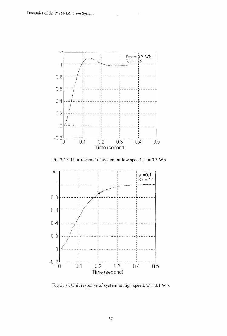
Fig 3.15, Unit respond of system at low speed, \jf = 0.3 Wb.
1
0.8
0.6
0.4
0.2
I I
- -·-----'
I I
I I ; p-=0.1
:Ks=1.2 ' ' --- T" ~.r::: . ..:::_.,--~~.....;
~~-7 : .: ~,.....~-~' : ,,,
--;_ ----7-·i- ----- -,- -------r - - - - - -
' // : ' '
--i-lc--- -~------ -;.----- --r------ -;/
;\
---- -~1- j- ----- -~ ------ -~ -------~ ------I '
/ ---J- --:- ----- --:- ----- - t - - - - - - - :- - - - - - -
! ' I
/'' 0 .,.·~---- ' ' ' - -,- - - - - - - -,- - - - - - - T - - - - - ' ---------'
-0.2~----~----~----~----~----~
0 0.1 0.2 0.3 0.4 0.5 Time (second)
Fig 3 .16, Unit response of system at high speed, \Jf = 0.1 Wb.
37
Dynamics of the PWM-IM Drive System
"I C! CJ c<r (xad)
()
_r; CJ 0
= ·-'
u
!\ : : '• N~~ :
- - - - - - - - -: - - - - - - - - - -:: - ~~ - - -- - """'"":"'""'""""'""""-' .... m ..... _.....,._,...._. ..... _. ....... ,_
idA
. ' " . . ' " . . ' " .
:;-Ti r r 1<:> ( s '=""-'"-' r 1 d)
._. ">
' ' ' - --- -- - - -·- - -- - -- -- ...I-- ----- - - L..- -- -----: :
: ... :-:. Tin-. P. (:=. P.c-.n n d')
\'t (Wbf---------.---------r--------,---------.
--- - - - - - _;_- - -- -- -- ~ - - ----- - - ~- -- - - ---. ' ' . ' '
0. 6 ln..- - - - - - - -l-- - ------ ~ -- -- -- --- ~- - - - - ---I \ . . .
() 4 1- J._- - - - - )_ - ------- j ------ --- L- - - - - -- -\., : . : ,_, ~ ~ ________ J ________ f' ____ : ~ _ -~L ~ _ _ _ _ _ _ I
(_) .2 r = : : 1 1:1 'I ::2 :::-. -~1
Tin-...:< ( s ..:<•= -=• n•:l)
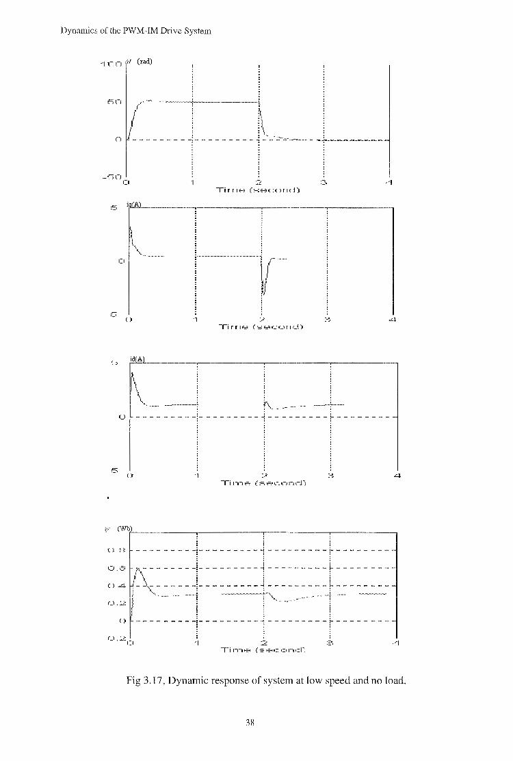
Fig 3.17, Dynamic response of system at low speed and no load.
38
Dynamic of the PWM-IM Drive System
1 ooffi.-~~_ad~)---------.-------------.------------.-------------.
50
0
-50 0
Tinoe (second)
~
·' iq(A)
t~,
\f --.... ~~N~-
u
)
r_~
C• -I 2 .:. 4 li r r 1-: ~ (•:<":ond)
~. i A
i\ ., ·,,
w - - i .. --~ ~
0 !"'"·~ ~··"
0 'I 2 :~. J'l Tin-..;:. (seoo: •:•n-=1·~
'!f' (W'b)
" '·' r------- -!- -- ----- -1\::;---~- o·c :y~ .:--~- -J Ql--------1---------1---------r--------J
- CJ ·.-:,.} -~ --( ) 1
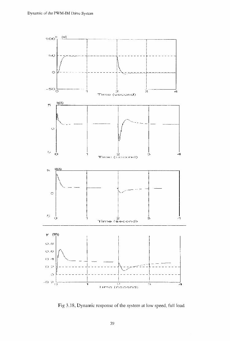
Fig 3.18, Dynamic response of the system at low speed, full load
39
Dynamics of the PWM-IM Drive System
2:'::· u''r'---"'r'-'ad=-) -----,.--------,---------,---------,
2UU . . .
--------~---------1---------r--------. . ' '
-------------------------------------. . . ·1 GO . . . . . . ' '
- ,~.::~::::-..:-:."::..=;- -·~j--------- L.--------! : !-., : . '........... . I I I N ~ 1
7' - - - - - - - -J- --------~ ---~~~ ... ~. ::_.::. -::_- -r ,__~~~-~~ : : :
'100
u . ' --------~---------~---------~--------
: : l . ' . . . . . -GO~--------~·--------~-------~·~------~
0 'I ·.?
TilliO.::.' (GC'CQiid)
:'::1 iq(A)
-__ ::-_ ~--- ------t -/::-::-:._ -:-- -~=-:-' ' . ' ' ' ' ' ' ' '
0 ., 2 Ti 1118 ( :=.8c.n11 cJ)
id A1
·-~ :2 Ti r r!Ho ( ~HC( H 1d)
~ (rWb~J~--------,-----------,------------~-----------.
1:1 ,;"?. ('\
L"J ~-; \
\ : : :
~=: .-:·: ~~~:··-·~~~~~-I~~~~~~~~ r ~ ~ ~)~ ~ ~-~-~ ~= ~ ~ ~ ~ ~ ~ () r -------- -!- --------j ~~ - -/ - ----l- -------i
~ ! ~~··/ ! -L-J ·? : : :
. u 1 2 ~-"' 4 1 1 rno ~oocona)
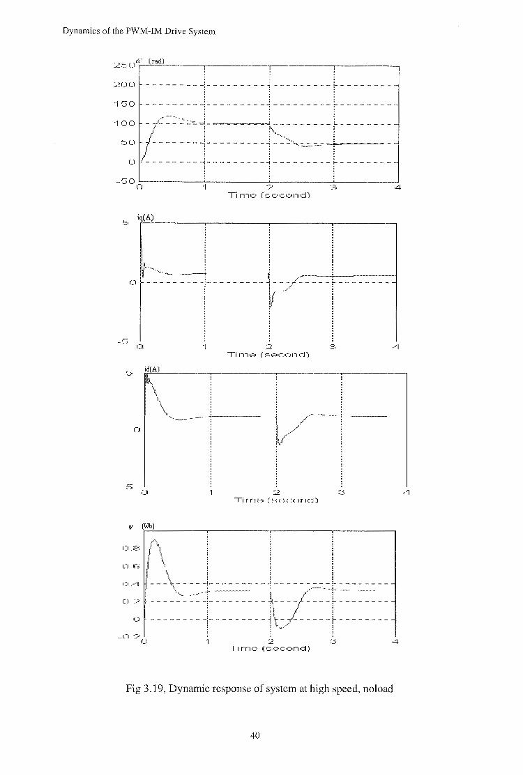
Fig 3.19, Dynamic response of system at high speed, no load
40
Dynamic of the PWM-IM Drive System
;>()()
·J () ()
. . --------~---------~---------. . . . . . - - - - - - - - -· - - - - - - ~ - - ..... - - - - - - - - -. . . . . . - -/"'-:: :_' ::_-:::. .=-....~-·- -
( : / i
---------~. :\ i \., ~~
J :
() .1_ - - - - - - - -i- - - - - - - - - -1 - - - - - - - - -
-bU ()
. . . .
'1
~ ~r(=A~)---------~--------~~--------~--------__,
~ : "~ fl-.. '-~---~ .. ~'''-nmm""'
CJ - - - - - - - - -~- - - - - - - - - v --------~ --------. . ' '
'
-G 4
. ~ t-- i /"'·,~-" :-() ---------:- --------1-r -------i- -------i :1/ : . . . .
-b () "1
\V (W.rb"----------~-------~------~-------,
(\ i i i 0 . 8 1 -\- - - - - - -i- - - - - - - - - ~ - - - - - - - - - ~ - - - - - - - -0 _E) 1- - ~~- - - - - _[_-- ------ ~--------- ~---- -- --
\ : : :
~= ::::~~~ctc:~~~J::;~J:~~ - - f : :1 I : 1 : !I :
0 - - - - - - - - -:- - - - - - - - -: ,/ - - - - - - - r ---------0.2 - ' ' ' --
0 1 2 3 4
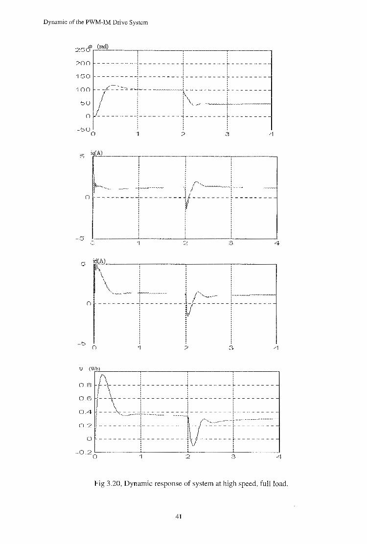
Fig 3.20, Dynamic response of system at high speed, full load.
41
Dynamic of the PWM-IM Drive System
3-4, Effects of digital implementation. As mentioned at the beginning of this chapter, this project employs an indirect control procedure that totally ignores the effects of the sampler and digital computer on the real time system. Therefore, this chapter will remain incomplete without some discussion of these effects on the dynamic response and steady sate error of the system. studies in [14] shows that there are two main factors that could influence on digital system: the sampling rate and quantisation error.
3-4-1, Sample rate: + Choice of sample rate : The selection of the best sample rates for a digital control system is a compromise. Generally, the performance of a digital control system improves with increasing sample rate, but cost may also increase with faster sampling. A decrease in sample rate means more time is available for the control calculation; hence, slower microcomputer are possible for a give function, or more control capability is available for a given microcomputer. Either result lower cost per function. For PWM-IM drive system with some AID converters, slower sampling means less conversion speed is required, which will also lower cost. Furthermore, it can be seen that faster sampling require a large word size, which would also increase cost. All these arguments suggest that the best choice is the lowest sample rate that meets all performance specification. + Sampling theory : The sampling theory [14] states that in order to reconstruct an unknown band-limited continuous signal from samples of that signal, the sample rate must be at least twice as fast as the highest frequency contained in that unknown signal. This theory applies to closed-loop PWM-IM drive system because reference motor speed co is considered as unknown signal that must be followed by the motor speed. Based on the sampling theory, the sample rate must be at least twice the required closed-loop bandwidth of that system, that is 40Hz for speed loop and 120Hz for current loops. If the sample rate is chosen lower than these limitation, the system would unstable or considerable slower than specification. + Time response and smoothness: The sample rate 40 Hz for speed loop and 120 Hz for currents loops provide the fundamental lower bound of the sample rate. In practice, however, these lower bounds would be judged far too slow for an acceptable time response. Therefore, It would be typical to chose a sample rate at 10 to 40 time of closed-loop bandwidth in order to limit the magnitude of the control steps. This means that the desired sample rate for a reasonable smooth time response for speed loop is 200 to 8000 Hz and current loops is 600 to 2400 Hz. + Command change delay : In addition to the smoothness issue, it is important to reduce the delay betvveen a command change and the system response to that command change. A command motor speed input can occur at any time through a sample period; therefore, there can be a delay up to full sample period before the controllers are aware of this change. For a system with human input such as IM drive system, the sample rate should be at least 20 time band width frequency in order to kept command delay time to be less than 10% of rise time.
42
Dynamic of the PWM-IM Drive System
+ Multirate sampling : It is useful to use different sample rate on the speed loop and current loops. By such a way, the system is called multirate (MR) system in which current loops (inner loops) are normally faster than speed loop (outer loop). The sample rate selection for multirate system is also carried out using discussion showed above. However, care should be taken in order to avoid an unacceptable movement of the inner roots [14/p508].
3-4-2, Quantisation effects : The fixed point is normally used to represent a number in digital calculation. Therefore, a number has to be quantised by either truncation or rounding process. It result in errors known as quantisation errors. Quantisation errors can have a detrimental effects on system performance at fast sample rate with a word size less than 10 bits. Therefore, it would be useful to analysis the system's sensitivity to quantisation errors and possibly to limit the sample rate to reduce sensitivity. Offcourse, another approach that can reduce the effects of quantisation errors is use of microcomputer with higher word size bits. Practically, the quantisation error is typically not an issue by using microcomputer with 16 or more bits.
As conclusion, this chapter discusses the dynamic of the PWM-IM transvertor control system. A model of system in the form of space-state vector is derived. A new method which employs the advantages of software simulink tool is introduced to determine parameter of controllers. Simulation of whole system shows that the couple induced voltages between d and q axis of motor influence strongly on performance of system and these effects change with change of the operation point of system. By tuning the set of parameters of controllers at most important points, the best set of control parameters can be chosen so that the worst-case system performance is acceptable. Finally, the effects of digital implementation is discussed. It expressed that the best sampling policy for system is a complicated matter involving compromise a mong many factors. Therefore, the analysis of sample rate tools to make the most costeffective choice are described.
43
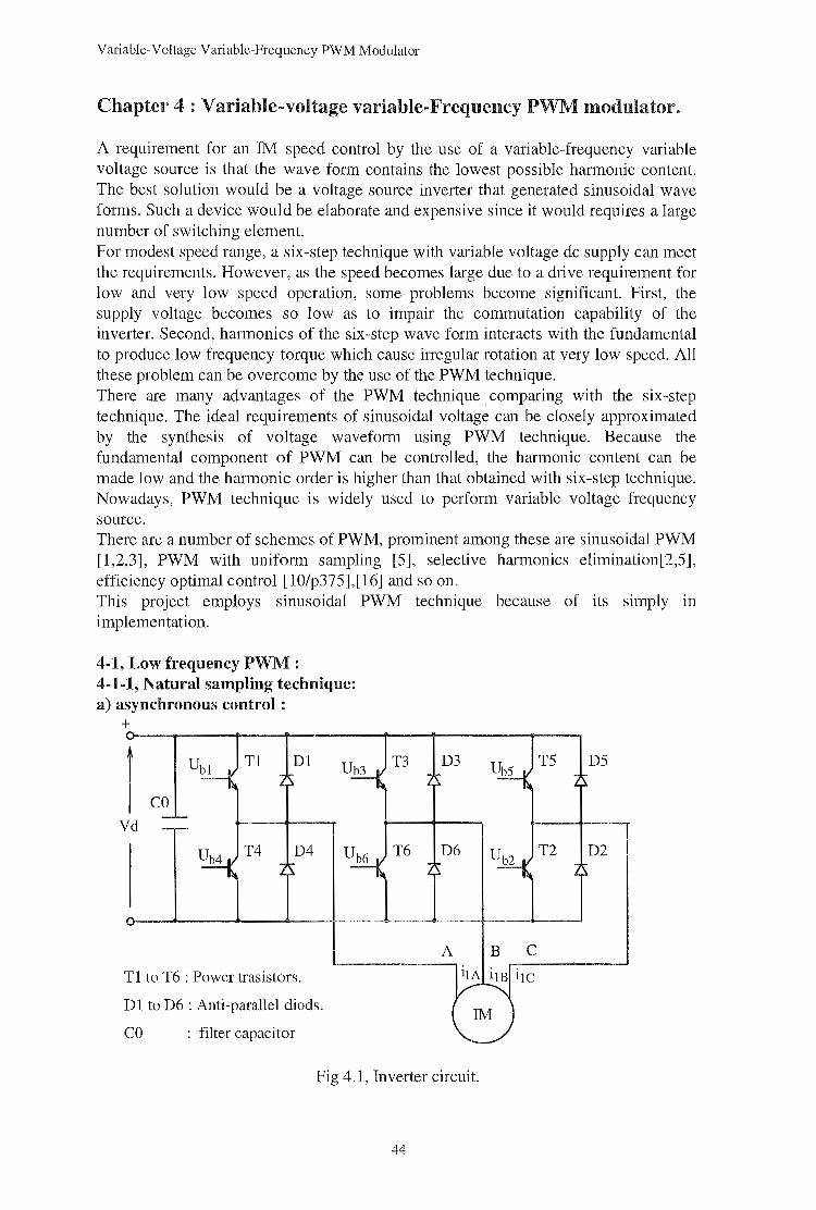
Variable-Voltage Variable-Frequency PWM Modulator
Chapter 4: Variable-voltage variable-Frequency PWM modulator.
A requirement for an IM speed control by the use of a variable-frequency variable voltage source is that the wave form contains the lowest possible harmonic content. The best solution would be a voltage source inverter that generated sinusoidal wave forms. Such a device would be elaborate and expensive since it would requires a large number of switching element. For modest speed range, a six-step technique with variable voltage de supply can meet the requirements. However, as the speed becomes large due to a drive requirement for low and very low speed operation, some problems become significant. First, the supply voltage becomes so low as to impair the commutation capability of the inverter. Second, harmonics of the six-step wave form interacts with the fundamental to produce low frequency torque which cause irregular rotation at very low speed. All these problem can be overcome by the use of the PWM technique. There are many advantages of the PWM technique comparing with the six-step technique. The ideal requirements of sinusoidal voltage can be closely approximated by the synthesis of voltage waveform using PWM technique. Because the fundamental component of PWM can be controlled, the harmonic content can be made low and the harmonic order is higher than that obtained with six-step technique. Nowadays, PWM technique is widely used to perform variable voltage frequency source. There are a number of schemes of PWM, prominent among these are sinusoidal PWM [1,2,3], PWM with uniform sampling [5], selective harmonics elimination[2,5], efficiency optimal control [10/p375],[16] and so on. This project employs sinusoidal PWM technique because of its simply in implementation.
4-1, Low frequency PWM: 4-1-1, Natural sampling technique: a) asynchronous control:
+
Tl to T6 : Power trasistors.
Dl to D6 :Anti-parallel diods.
CO : filter capacitor
T3 D3
T6 D6
A B C
Fig 4.1, Inverter circuit.
44
T5 D5
T2 D2
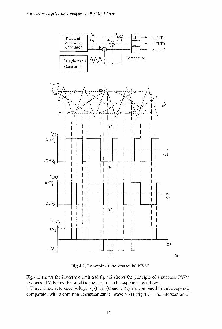
Variable-Voltage Variable-Frequency PWM Modulator
Referent Sine wave Generaror
Triangle wave
Generator
I . - - I
: I I I
I I r-- I
--1 -~1 I I
I I
I i I
I 1 I I
I I
I -I
I I I I I I I
I I I I I I I
I I I
va
Vb
Vc +
¥A
I I I I I I ICa) I I
I I '--I I I I
I I I I
I I I
: : l(b)l
I I I I I I I
I I I I I I
I I I
'-- I I I l(c)l I I I I I I I I I I I I I I . I
(d)
I I
I I
I I
Comparator
1--1
I I I
to Tl,T4
to T3,T6
to T5,T2
I I
I
I 'r--:-
I I I cot
I f--- I I I I I I I -l-1
I I
I -I
I I I I I I I I I
I
I r-
I I
I co
I
cot
Fig 4.2, Principle of the sinusoidal PWM
(J)
Fig 4.1 shows the inverter circuit and fig 4.2 shows the principle of sinusoidal PWM to control IM below the rated frequency. It can be explained as follow : + Three phase reference voltage v a ( t) , v b ( t) and v c ( t) are compared in three separate comparator with a common triangular carrier wave v 1 ( t) (fig 4.2). The intersection of
45
Variable-Voltage Variable-Frequency PWM Modulator
the reference voltage and carrier signal determine both the onset and duration of the modulated pulse and hence the pulse pattern. The circuitry actuating the turn-on and turn-off of the transistor inverter is controlled by sensing these intersections. +To calculate vAn (t), let consider the operation of switch pairs (T1,T4) and (T3,T6):
-T1,T4: Tl is on when va(t)>vt(t). T4 is on when va(t)<vt(t). This produces phase voltage v Ao(t)as fig 4.2 (b).
- T3,T6: T3 is on when vb(t)>vJt). T6 is on when vb (t)<vt (t). This produces phase voltage vn0 (t) as fig 4.2 (c).
- Line Voltage : VAB(t)= VA0 (t)-Vn0 (t) asfig4.2(d).
+ If m is module index :
and p is frequency module index :
where fc =carrier frequency. f1 = reference frequency.
(4.1)
(4.2)
reference [2/p299] shows that for m:::;; 1, the fundamental component in the phase voltage waveform v Ao(t) is given by:
V =mvcl AOJ 2-!2
(4.3)
Form> 1 (known as overmodulaton), the relationship between v Am (t) and module index m is no longer linear. Form>> 1, PWM reaches six step mode and the fundamental component of VA01
reaches the maximum value :
v_ = Jivcl · AUl-max (4.4)
1t
From Eq (2.29), the amplitude of v AOJ (t)can be controlled by changing modulation index m, ie by changing V m if VT is fixed, and the frequency of v Am ( t) can be controlled by changing frequency of the reference waveform. Obviously, the frequency index p should be large to reduce the effects of harmonics. However, the maximum value of p is limited by switch capability of power devices.
46
Variable-Voltage Variable-Frequency PWM Modulator
b) synchronous control : At asynchronous control shown above, the variable frequency variable amplitude sine wave is compared with a triangular waveform of fixed frequency. In this case, the carrier waveform is asynchronous with modulating wave. The quantity of the output waveform will depend on the modulating index m. The highest this ratio, the highest will be the frequency of the unwanted harmonics in the output waveform, and the ripple current that is produced in an inductive load such as IM will be less. The draw back to this waveform generation method is that the carrier and modulating frequency are generally incommensurable so that the PWM wave is non-periodic and therefore contain components of lower frequency than wanted frequency component (subharmonics). The flux produced by the subharmonics may be considerable and can seriously interfere with the efficient operation of the IM. The speed of currently available BJT's and MOSFET's and the losses associated with the switching of these devices have made the higher carrier to modulating frequency impractical. It has thus been necessary to devise other way of avoiding the generation of the subharmonics in the output waveform. One way this can be achieved is by synchronising the carrier and modulating wave so that the carrier frequency is an integer multiple of the modulation frequency. A more detailed analysis indicates that the frequencies of the reference and carrier wave should satisfy the following relation
n:2:1 (4.5)
The PWM waveform is than periodic and contains only harmonics which are integer multiple of fundamental. The difficulties with synchronous operation is that the carrier and modulating wave are synchronised . Therefore, the carrier frequency must vary over wide range as the output frequency. However, it is not usually practical to allow the carrier frequency to vary so widely, since, if it is too low, the motor time constant is insufficient for adequate smoothing of the motor current, and if it is too high, the inverter commutation losses are unacceptably large. To overcome this problem, the modulating index is changed at interval throughout the operating range of the motor speed in order to keep the carrier frequency within prescribed limit. This method is known as sliding mode and will be discussed in more detail at the end of this chapter.
2-1-2, Uniform sampling technique The natural sampling technique of the sinusoidal PWM has found wide acceptance for controlling electronic switching power inverter. PWM control signals were originally generated with the help of electronic hardware, but lately, microcomputer has begun to play an important role in the design of control signal generator for power inverters gradually assuming more and more functions. The microcontroller-based PWM have been developed principally on the basis of the look-up table. In the natural sampling technique, the number of notch angles for a wave pattern tends to increase at lower fundamental frequency and the number of wave patterns stored tends to be limited. Even if the memory size is considered to be no constraint, the hardware and software designs of the present modulator are such they often do not provide good angle resolution, and the output wave do not respond adequately in real time with change in voltage and frequency commands. Although
47
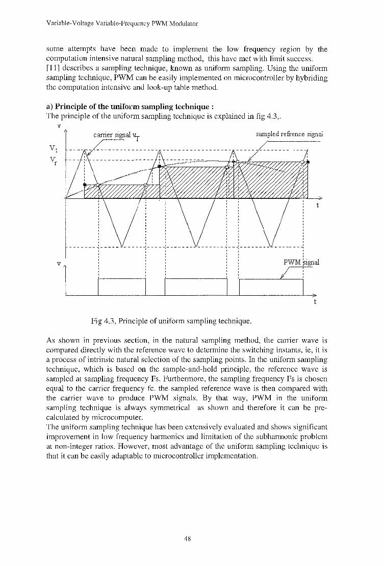
Variable-Voltage Variable-Frequency PWM Modulator
some attempts have been made to implement the low frequency region by the computation intensive natural sampling method, this have met with limit success. [11] describes a sampling technique, known as uniform sampling. Using the uniform sampling technique, PWM can be easily implemented on microcontroller by hybriding the computation intensive and look-up table method.
a) Principle of the uniform sampling technique : The principle of the uniform sampling technique is explained in fig 4.3,.
v carrier signal 'T sampled refrence signal
' -------,-----' '
-----~----~-------
t
' -------~--~--------
vl~----~------~--~--------~~-------,1-P_W_M~~-ign~: t
Fig 4.3, Principle of uniform sampling technique.
As shown in previous section, in the natural sampling method, the carrier wave is compared directly with the reference wave to determine the switching instants, ie, it is a process of intrinsic natural selection of the sampling points. In the uniform sampling technique, which is based on the sample-and-hold principle, the reference wave is sampled at sampling frequency Fs. Furthermore, the sampling frequency Fs is chosen equal to the carrier frequency fc. the sampled reference wave is then compared with the carrier wave to produce PWM signals. By that way, PWM in the uniform sampling technique is always symmetrical as shown and therefore it can be precalculated by microcomputer. The uniform sampling technique has been extensively evaluated and shows significant improvement in low frequency harmonics and limitation of the subharmonic problem at non-integer ratios. However, most advantage of the uniform sampling technique is that it can be easily adaptable to microcontroller implementation.
48
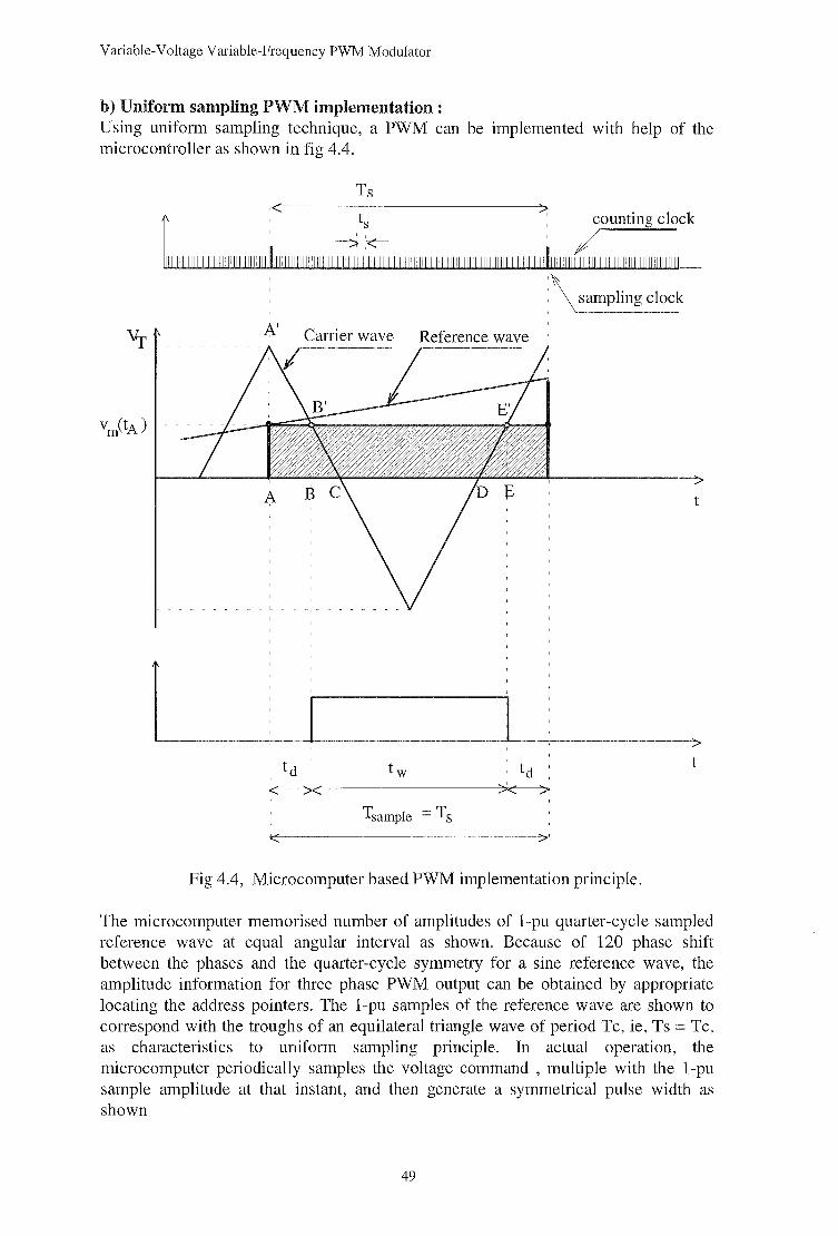
Variable-Voltage Variable-Frequency PWM Modulator
b) Uniform sampling PWM implementation : Using uniform sampling technique, a PWM can be implemented with help of the microcontroller as shown in fig 4.4.
1
Ts
[
: ts : counting clock
Ulllllllllllllllllllllllllllllllllll~lllllllllllllllllliii~II:I;IIIIIIIIIIIIIIIIIIIIIIIIIIIIIIIIIIIIIIIIIIIIIIIIIIIIIIIIIIJIIIIII~IIIIIIIIIIIIIIIIIIIIIIIIIII :\sampling clock
A' Carrier wave Reference wave
t
- - L -
> td ' tw td
t
< >< :>.....~ '
Tsample = Ts
7'
Fig 4.4, Microcomputer based PWM implementation principle.
The microcomputer memorised number of amplitudes of 1-pu quarter-cycle sampled reference wave at equal angular interval as shown. Because of 120 phase shift between the phases and the quarter-cycle symmetry for a sine reference wave, the amplitude information for three phase PWM output can be obtained by appropriate locating the address pointers. The 1-pu samples of the reference wave are shown to correspond with the troughs of an equilateral triangle wave of period Tc, ie, Ts = Tc, as characteristics to uniform sampling principle. In actual operation, the microcomputer periodically samples the voltage command , multiple with the 1-pu sample amplitude at that instant, and then generate a symmetrical pulse width as shown
49
Variable-Voltage Variable-Frequency PWM Modulator
Fig 4.4 shows operation of PWM modulator principle within only one sample reference wave v m. Here :
Ts = sample interval of reference wave. ts = basic clock pulse. td = delay time of PWM. tw = pulse width time.
The clock pulse with frequency fs= 1/ts can be created by a programmable counter. There are two problem concerning with clock pulse counter fs:
1, frequency fs must be large enough to ensure precision synthesis of the PWM wave. In each sample interval Ts, it should be at least 256 pulses.
2, How many pulse required to count sample time Ts, pulse width time tw and delay time td?
a) Sample time Ts :
T f f f N =~=~=~=-s TS ts Fs fc af1
where N Ts = number of clock pulse to count Ts. b) Pulse width time tw : From fig 4.4,
BE=2BC+CD Because:
hence:
BC= BB' *AC AA'
AC=AF 4
BE=2 BB' *AC+CD= AF (BB' +1) AA' 2 AA'
or:
CD=AF 2
(4.6)
(4.7)
(4.8)
N = 0 5N (vr(ta) + 1) (4.9) tw • Ts V
T
where : v r ( ta) = amplitude of sampled reference at t = t(A) V1 =maximum amplitude Of VT (15V) N tw = number of clock pulse required to count tw.
c) Delay time td: From 4.7, the number of clock count is easily driven:
(4.10)
c, Uniform sampling technique at asynchronous mode : At low frequency, PWM should operate at asynchronous mode to improve performance as explained in section 4-1-1, The exploded view of part of cycle in this mode is shown in fig 4.5, which is somewhat self-explanatory.
50
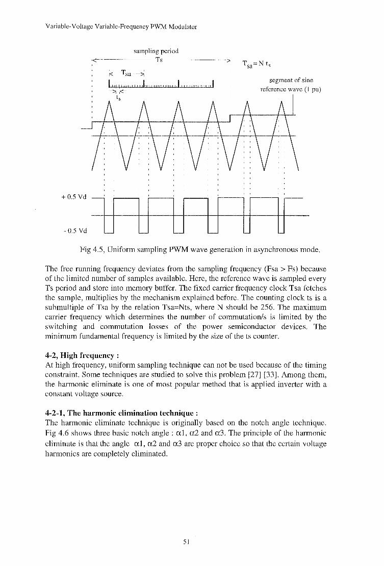
Variable-Voltage Variable-Frequency PWM Modulator
+ 0.5 Vd
-0.5 Vd
sampling period c.<------- Ts
lll!!llll!l!ll!!l!!l!!!!!l!!!!ll!!!!!!!!!!!!!!l!!!lll!!l!!lll!!ll!!!!!l!!!!ll
~ ;<-ts
iJ u u u ~
segment of sine reference wave (1 pu)
Fig 4.5, Uniform sampling PWM wave generation in asynchronous mode.
The free running frequency deviates from the sampling frequency (Fsa > Fs) because of the limited number of samples available. Here, the reference wave is sampled every Ts period and store into memory buffer. The fixed carrier frequency clock Tsa fetches the sample, multiplies by the mechanism explained before. The counting clock ts is a submultiple of Tsa by the relation Tsa=Nts, where N should be 256. The maximum carrier frequency which determines the number of commutation/s is limited by the switching and commutation losses of the power semiconductor devices. The minimum fundamental frequency is limited by the size of the ts counter.
4-2, High frequency : At high frequency, uniform sampling technique can not be used because of the timing constraint. Some techniques are studied to solve this problem [27] [33]. Among them, the harmonic eliminate is one of most popular method that is applied inverter with a constant voltage source.
4-2-1, The harmonic elimination technique: The harmonic eliminate technique is originally based on the notch angle technique. Fig 4.6 shows three basic notch angle: al, a2 and a3. The principle of the harmonic eliminate is that the angle al, a2 and a3 are proper choice so that the certain voltage harmonics are completely eliminated.
51
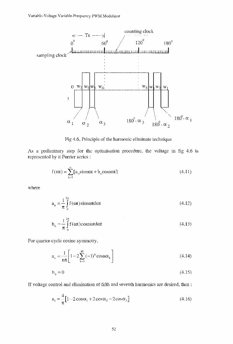
Variable-Voltage Variable-Frequency PWM Modulator
counting clock k-- Ts -~
. /L""""""""III"'""''"~~:,,,,,,,L,,,,,,,:,~::,,,III"""""'"'"':,~r sampling clocK , , ' '
0 180 - ex 2
0 180- ex 1
Fig 4.6, Principle of the harmonic eliminate technique
As a preliminary step for the optimisation procedure, the voltage in fig 4.6 is represented by it Furrier series :
where
=
f (cot)= ~)ansinncot + bncosncot] n=l
1 21t
an = - f f (cot) sinncotdcot 1t 0
1 21t
bn =- J f(rot)cosncotdcot 1t 0
For quarter-cycle cosine symmetry,
an= -1-[1 +2 i ( -1)kcosnexk]
nn k=l
b =0 n
(4.11)
(4.12)
(4.13)
(4.14)
(4.15)
If voltage control and elimination of fifth and seventh harmonics are desired, then :
(4.16)
52
Variable-Voltage Variable-Frequency PWM Modulator
4 a5 = -[1- 2cos5a1 + 2cos5a2 - 2cos5a,J = 0
5n ·
4 a7 = -[1- 2cos7a1 +2cos7a2 - 2cos7a3 ] = 0
n
(4.17)
(4.18)
Equation( 4.16) and ( 4.18) are solved to generate the look-up table and stored in memories. Again, because of the symmetry and absence of notch in the middle of the wave, only the pattern for the 0 - 60 segment need be stored , and three phase full wave PWM outputs can be generated by appropriately locating address pointer. Studies in [17] shows that the maximum magnitude of the fundamental is only about 93 percent for complete elimination of the fifth and seventh harmonics. As a result of elimination of lower order harmonics, the higher order significant harmonics such as eleventh and thirteenth become prominent. An improvement performance can be obtained by solving harmonic heating loss for different harmonics as a function of the notch angles and then iterating the angles so that loss (ie. the rms ripple current ) is minimum. The effects resistance, though, varies as a function of temperature, and skin effect is assume to be constant. The harmonic eliminate operation typically extend from 80 percent of the fundamental voltage, and the wave pattern characterised by the a angles are stored in 1 percent increment which may be adequate for system requirements. The lower step size is limited by the resolution of a angle implementation. At about 93 percent of fundamental voltage, a1 approaches to zero, and from this point, the voltage is increased by a one percent step by symmetrically shifting the notch toward the edge of half cycle and simultaneously reducing their widths
4-2-2, PWM operation modes. According to discussions in obvious sections, the modes of PWM-IM operation will now be described with the help of fig 4.10 : * a< a1 : fl is lower than rated frequency of IM. PWM operates in the asynchronous mode. The carrier frequency fc is maintained as highest as possible to reduce effects of harmonics. * a= a1 : frequency modulation index preaches limited value. Therefore, fc must be reduced to fc 1. However, fc 1 must be sufficiently large to maintain a nearly sinusoidal motor current. * al < a < a2 : the system shifts to synchronous mode, ie fc is changed synchronously with f1 at a constant ratio p 1. * a = a2 : the fc become large enough to violate the minimum notch time restriction. Therefore, fc must be reduced. * a2 < a < a3 : system also operates in synchronous mode but ratio between fc and f1 is changed to p2. * a = a3 : the operation is brought close to the boundary of the sinusoidal PWM, ie m "" 1. From this, the system is shifted to harmonic elimination mode The project employs a single microcontroller M68HC11 with speed of 2 kHz. Therefore, the maximum carrier frequency fc is also limited by capability for control calculation time of M68HC11. Estimated processing time for both feedback control function and PWM modulator is 1000!-LS ( see also chapter 6 - System software implementation). Here, the maximum fc is limited within 1000 Hz, or 1KHz. As
53
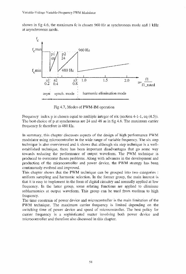
Variable-Voltage Variable-Frequency PWM Modulator
shown in fig 4.6, the maximum fc is chosen 960Hz at synchronous mode and 1 kHz at asynchronous mode.
a1' a2 0.2: 0.4
a3' 1.0 0.8:
1.5 2.0
: asyn synch. mode , harmonic elimination mode
Fig 4.7, Modes ofPWM-IM operation
f1 a=
fl_rated
Frequency index pis chosen equal to multiple integer of six (section 4-1-1, eq (4.5)). The best choice of p at synchronous are 24 and 48 as in fig 4.6. The maximum carrier frequency fc therefore is 480 Hz.
In summary, this chapter discusses aspects of the design of high performance PWM modulator using microcontroller in the wide range of variable frequency. The six step technique is also overviewed and it shows that although six step technique is a wellestablished technique, there has been important disadvantages that go some way towards reducing the performance of output waveform. The PWM technique is produced to overcome theses problems. Along with advances in the development and production of the microcontroller and power device, the PWM strategy has been continuously evolved and improved. This chapter shows that the PWM technique can be grouped into two categories : uniform sampling and harmonic selection. In the former group, the main interest is that it is easy to implement in the form of digital circuitry and normally applied at low frequency. In the latter group, some relating functions are applied to eliminate subharmonics at output waveform. This group can be used from medium to high frequency. The time constrain of power device and microcontroller is the main limitation of the PWM technique. The maximum carrier frequency is limited depending on the switching time of power device and speed of microcontroller. The best policy for carrier frequency is a sophisticated matter involving both power device and microcontroller and therefore also discussed in this chapter.
54
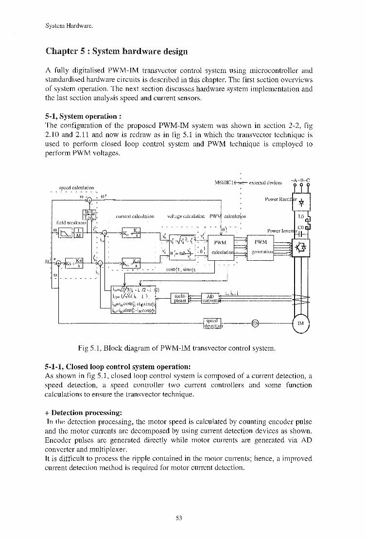
System Hardware.
Chapter 5: System hardware design
A fully digitalised PWM-IM transvector control system using microcontroller and standardised hardware circuits is described in this chapter. The first section overviews of system operation. The next section discusses hardware system implementation and the last section analysis speed and current sensors.
5-1, System operation : The configuration of the proposed PWM-IM system was shown in section 2-2, fig 2.10 and 2.11 and now is redraw as in fig 5.1 in which the transvector technique is used to perform closed loop control system and PWM technique is employed to perform PWM voltages.
M68HC1 ±~ external devices -A-B-C speed calculation
current calculation voltage calculation PW calculat(on
Fig 5.1, Block diagram of PWM-IM trans vector control system.
5-1-1, Closed loop control system operation: As shown in fig 5.1, closed loop control system is composed of a current detection, a speed detection, a speed controller two current controllers and some function calculations to ensure the transvector technique.
+ Detection processing: In the detection nrocessin£. the motor sneed is calculated bv counting encoder nulse
..L '-'" ..L ., ~ ..L
and the motor currents are decomposed by using current detection devices as shown. Encoder pulses are generated directly while motor currents are generated via AD converter and multiplexer. It is difficult to process the ripple contained in the motor currents; hence, a improved current detection method is required for motor current detection.
53
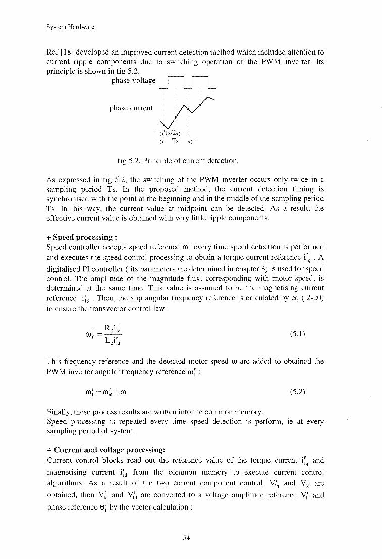
System Hardware.
Ref [18] developed an improved current detection method which included attention to current ripple components due to switching operation of the PWM inverter. Its principle is shown in fig 5 .2.
phase voltage ~
phase current
-->:r's/2'<(-- : -; Ts '<-
fig 5 .2, Principle of current detection.
As expressed in fig 5.2, the switching of the PWM inverter occurs only twice in a sampling period Ts. In the proposed method, the current detection timing is synchronised with the point at the beginning and in the middle of the sampling period Ts. In this way, the current value at midpoint can be detected. As a result, the effective current value is obtained with very little ripple components.
+ Speed processing : Speed controller accepts speed reference cor every time speed detection is performed and executes the speed control processing to obtain a torque current reference i~q . A
digitalised PI controller (its parameters are determined in chapter 3) is used for speed control. The amplitude of the magnitude flux, corresponding with motor speed, is determined at the same time. This value is assumed to be the magnetising current reference i~ct . Then, the slip angular frequency reference is calculated by eq ( 2-20) to ensure the transvector control law :
(5.1)
This frequency reference and the detected motor speed co are added to obtained the PWM inverter angular frequency reference co~ :
Finally, these process results are written into the common memory. Speed processing is repeated every time speed detection is perform, re at every sampling period of system.
+ Current and voltage processing: Current control blocks read out the reference value of the torque current i~q and
magnetising current i~ct from the common memory to execute current control algorithms. As a result of the two current component control, v:~ and Vtct are
obtained, then V1~ and v:~ are converted to a voltage amplitude reference Vt and
phase reference 8~ by the vector calculation :
54
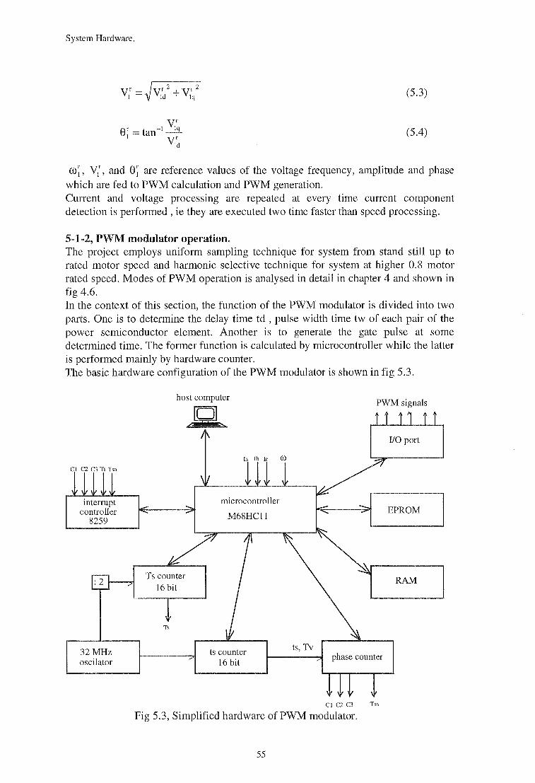
System Hardware.
yr = ~yr 2 yr 2 I ld + lq
yr er _ t -1 lq
1 - an-Vtct
(5.3)
(5.4)
w~, V1r, and 8~ are reference values of the voltage frequency, amplitude and phase which are fed to PWM calculation and PWM generation. Current and voltage processing are repeated at every time current component detection is performed , ie they are executed two time faster than speed processing.
5-1-2, PWM modulator operation. The project employs uniform sampling technique for system from stand still up to rated motor speed and harmonic selective technique for system at higher 0.8 motor rated speed. Modes of PWM operation is analysed in detail in chapter 4 and shown in fig 4.6. In the context of this section, the function of the PWM modulator is divided into two parts. One is to determine the delay time td , pulse width time tw of each pair of the power semiconductor element. Another is to generate the gate pulse at some determined time. The former function is calculated by microcontroller while the latter is performed mainly by hardware counter. The basic hardware configuration of the PWM modulator is shown in fig 5.3.
Cl C2 C3 Ts Tsa
interrupt controller
8259
32MHz oscilator
host computer
)gL,
ts counter 16 bit
PWM signals
I/0 port
EPROM
RAM
phase counter
Cl C2 C3 Tsa
Fig 5.3, Simplified hardware of PWM modulator.
55
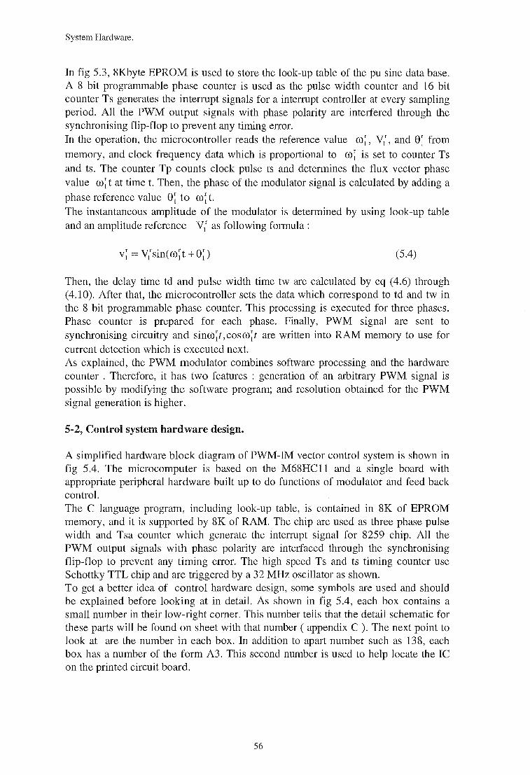
System Hardware.
In fig 5.3, 8Kbyte EPROM is used to store the look-up table of the pu sine data base. A 8 bit programmable phase counter is used as the pulse width counter and 16 bit counter Ts generates the interrupt signals for a interrupt controller at every sampling period. All the PWM output signals with phase polarity are interfered through the synchronising flip-flop to prevent any timing error. In the operation, the microcontroller reads the reference value ro~, Vt, and 8~ from memory, and clock frequency data which is proportional to ro~ is set to counter Ts and ts. The counter Tp counts clock pulse ts and determines the flux vector phase value ro; t at time t. Then, the phase of the modulator signal is calculated by adding a phase reference value 8~ to ro~ t. The instantaneous amplitude of the modulator is determined by using look-up table and an amplitude reference V1r as following formula :
(5.4)
Then, the delay time td and pulse width time tw are calculated by eq (4.6) through ( 4.1 0). After that, the microcontroller sets the data which correspond to td and tw in the 8 bit programmable phase counter. This processing is executed for three phases. Phase counter is prepared for each phase. Finally, PWM signal are sent to synchronising circuitry and sinro~ t, cos ro;· t are written into RAM memory to use for current detection which is executed next. As explained, the PWM modulator combines software processing and the hardware counter . Therefore, it has two features : generation of an arbitrary PWM signal is possible by modifying the software program; and resolution obtained for the PWM signal generation is higher.
5-2, Control system hardware design.
A simplified hardware block diagram of PWM-IM vector control system is shown in fig 5.4. The microcomputer is based on the M68HC11 and a single board with appropriate peripheral hardware built up to do functions of modulator and feed back control. The C language program, including look-up table, is contained in 8K of EPROM memory, and it is supported by 8K of RAM. The chip are used as three phase pulse width and Tsa counter which generate the interrupt signal for 8259 chip. All the PWM output signals with phase polarity are interfaced through the synchronising flip-flop to prevent any timing error. The high speed Ts and ts timing counter use Schottky TTL chip and are triggered by a 32 MHz oscillator as shown. To get a better idea of control hardware design, some symbols are used and should be explained before looking at in detail. As shown in fig 5.4, each box contains a small number in their low-right corner. This number tells that the detail schematic for these parts will be found on sheet with that number (appendix C). The next point to look at are the number in each box. In addition to apart number such as 138, each box has a number of the form A3. This second number is used to help locate the IC on the printed circuit board.
56
,..... ,..... 0
"!"'"-
[}= =
BUFFER ---r> HC245
(A2)
-v- LE
M68HC11AO
ADO ..I. AO-A7 PEl to --•? LATCH -AD? HCI38 PE2
(AI)
PE3 AS LE
-PE5 IRQ
RfW
:It~ R
I~ PES E
ADS A8-A15 to
AD15
lko 4
osc~
____j 32MHz
(Al9)
32MHz
"1=----16MHZ ~ ....._ > 74F74
(A20)
r- L-n
DO-D7 DATA BUS
" r-- PWMSIGNALS
ff Tv / > 74F74 i==
" ~'0~"'""_1\ IJO PORT _j - / ff >
i==
" ff wv 8255 r- I> 74F74 / >
ff • ~ ~ " EPROM / 4* " (A7) ~
L:= I> 74F74 / ff i==
r- ..lL " ff / '---
Ill I I I --# INTERUPT COUNTER COUNTER
A' DECODE
~ ~ 8259 8254 8254
HC138 EPROM - -(A3)
~ I !Rf''1Al ~ w IIA2 ~ IW I IA2 (AS)
E CS! r---r---
f.B--- " "" "<~::::~, '-'\. ~ ~' -, ::-.::
,, R!W ~ INTERU:l[ C-PHASE! ~ C-PHASE2
C-TVJ j
L RfW - LATCH LATCH C-TV2 j)o- HC373 HC373
A5 SE 1 r. (A12) (A13) Tv
ECODER
f~Y: ~ r-- MONO- -'
I I 1111 Ill I I HC!38 RAM! STABLE HC221
(A4)
~~ 32MHz COUNTER coutrrnR
~ (A9) - 74F193(2) 74Fl93(2)
A (A14,Al5) (A16,A17)
v 'I
"" "" "" "" @, ::s"' "::-.::'"~'\~~
RfW ~ ... ]t ~ • ~ C-TCl j
RAM2 RfW ' ......... LATCH L LATCH C-T 2 .v:- HC373 HC373
(AiD) (A21) (A22)
- MONO-
I I 1111 Ill I II STABLE HC221
16MHz COUNTER COutrTER - HC173(2) HC173(2) Tc
CONTROL BUS (A23,A24) (A23,A24) h
v v v y
ADDRESS BUS
Fig 5.4, Detail block diagram of PWM modulator

System Hardware.
5-2-1, Overview of control system hardware. The first part to look at in fig 5.4 is the M68HC11 microcontroller. The M68HC11 microcontroller accepts and processes speed and current feed back signals and motor speed reference from host computer or ROC. Then it produces address bits and data bits depending the function it is executing. The next parts to look for in the block diagram of the control system hardware are address latch ( A1) and data buffer (A2). Address latch is needed to grab address information produced by microcontroller. A heavy black line is used to distinguish the demultiplexer address bus from data bus. Following the address line to the of the address latch to find memory of the system (A7 to AlO) and memory decoder A3. The memory decoder connected to EPROM/RAM memory has two related purposes. The first is to produce a signal which turns on the desired EPROM or RAM. The second purpose is to make sure that only once device is outputting on data bus at a time. The box just below memory decode is port decoder A4 that has somewhat the same purpose with memory decoder. However, it is used for decoding external device such as phase counter, interrupt controller, etc. A set of latches A12, A13 and 4 bit counters A14 to A17 performs 16 bit counter while another set from A18 to A 21 performs 16 bit Ts counter. The output pulses of ts and Ts counter are put through monostable to expand their duration before sent to phase counter A12. System output is expressed on the top of the diagram. It includes a programmable parallel port, and six flip-flop to synchronising output waveforms. Finally, six optoisolation are used to isolate control system from power inverter to avoid any damage.
5-2-2, M68HC11AO controller: (fig 5.5) Power supply : connected to pin Vdd (+5V) and Vss (ground). The 1~F capacitor (C6) and 0.01 ~F capacitor (C4) are used to provide good power supply bypassing at the MCU. Both these capacitor should be as close (physically and electrically) as possible to the M68HC11AO and should have good high-frequency characteristics (ie, not old technology dipped ceramic disc). The separate 0.01 ~F capacitor is included because the large l~F capacitor is typically not as good at snubbing very high frequency noise. The 1 ~F capacitor (C5) primarily supplies charge for bus switching through a very low impedance path. Without this bypass, there could be very large voltage drops in the circuit-board runner to the MCU due to the very high current spike caused by several MCU pins simultaneously switching from one level to the other. Mode select pin (MODB/VSTBY and MODAILIB) : Because MCU is used in the expanded mode, the mode select pins MODB an MODA must be high. To do this, 4.7K resistor Rll and R12 are used. Hovvever, a connect Jumper Jl could be used to pull MODB down for test mode. Crystal oscillator pins (EXTAL and XTAL): a crystal oscillator of 8 MHz is used. The resister R13110M provides direct current bias to the inputs. Two equal capacitor C1 and C2118pF are combined with the higher output impedance in order to limit the power into the crystal. Clock pin (E) : is the bus frequency clock output and four time lower than crystal frequency (equal to 2 MHz in this case). This pin can be used to control external
58
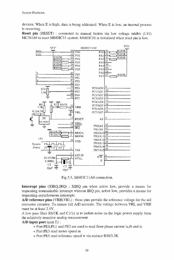
System Hardware.
devices. When E is high, data is being addressed. When E is low, an internal process is occurring. Reset pin (RESET) : connected to manual button via low voltage inhibit (LVI) MC34164 to reset M68HC11 system. M68HC11 is initialised when reset pin is low.
vee M68He11AO 20 PDQ
w
1-'------'1'-'-17 RESET
---.-:..1~8 XIRQ ----'-1"-19 IRQ
P'-'-'-'..:..:..:..:r=:-:r-"3'-l MODA L:..:;.;:.::::...;:..:..:...::;.;r---,.....:2'-l MODB
+5v -.,---..-----,----.---"2""'16 VDD
System Power
y---+---1.---1---"-J vss ..-------!.-1 EXTAL t---c:==J-T'-1 XT AL
PeO/ADO Pe1/AD1 Pe2/AD2 Pe3/AD3 Pe4/AD4 Pe5/AD5 Pe6/AD6 Pe7/AD7
AS
PBO/A8 PB1/A9 PB2/A1 PB3/A11 PB4/A12 PB5/Al3 PB6/Al PB7/A15
R/W E
9 10 11 12 13 14 15 16
4
42 41 40 39 38 37 36 35
6 5
Fig 5.5, M68HC11AO connection.
vee
Interrupt pins (XIRQ,IRQ) : XIRQ pin when active low, provide a means for requesting nonmaskable interrupt whereas IRQ pin, active low, provides a means for requesting asynchronous interrupts. AID reference pins (VRH,VRL) :these pins provide the reference voltage for the aid converter circuitry. To ensure full AJD accurate. The voltage between VRL and VRH must be at least 2.5V. A low pass filter R611K and Cl/lu is to isolate noise on the logic power supply from the relatively sensitive analog measurement. AID input port (port E) :
+Port PEO,PEl and PE2 are used to read three phase current ia,ib and ic. + Port PE3 read motor speed ffi. +Port PES read reference speed w via resistor R10/3.3K
59
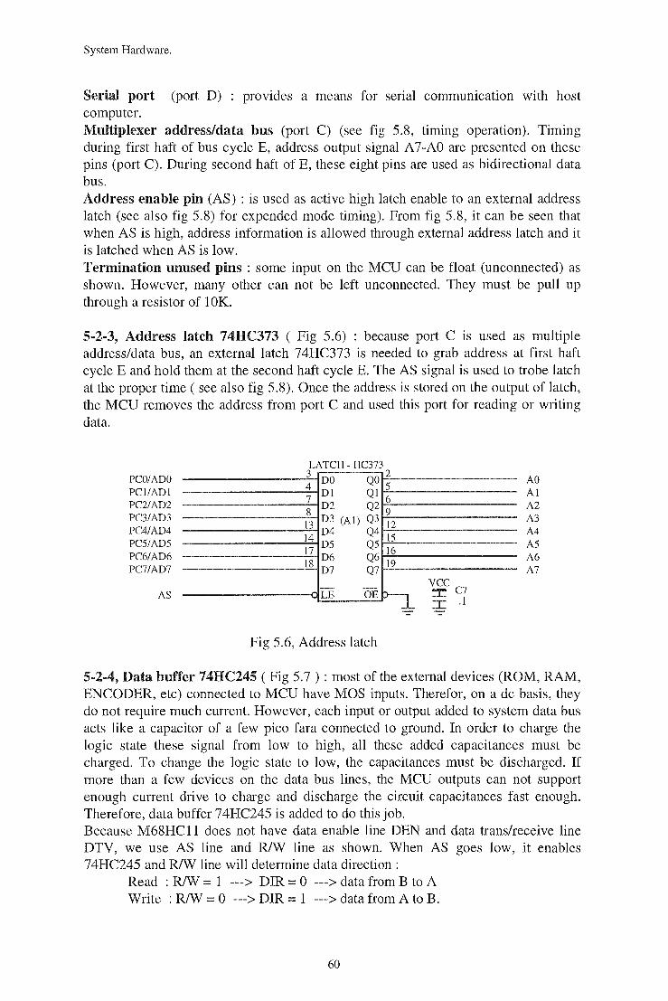
System Hardware.
Serial port (port D) : provides a means for serial communication with host computer. Multiplexer address/data bus (port C) (see fig 5.8, timing operation). Timing during first haft of bus cycle E, address output signal A7-AO are presented on these pins (port C). During second haft of E, these eight pins are used as bidirectional data bus. Address enable pin (AS) : is used as active high latch enable to an external address latch (see also fig 5.8) for expended mode timing). From fig 5.8, it can be seen that when AS is high, address information is allowed through external address latch and it is latched when AS is low. Termination unused pins : some input on the MCU can be float (unconnected) as shown. However, many other can not be left unconnected. They must be pull up through a resistor of 1 OK.
5-2-3, Address latch 74HC373 ( Fig 5.6) : because port C is used as multiple address/data bus, an external latch 74HC373 is needed to grab address at first haft cycle E and hold them at the second haft cycle E. The AS signal is used to trobe latch at the proper time (see also fig 5.8). Once the address is stored on the output of latch, the MCU removes the address from port C and used this port for reading or writing data.
PCO/ADO PCI/ADl PC2/AD2 PC3/AD3 PC4/AD4 PC5/AD5 PC6/AD6 PC7/AD7
AS
LATCH- HC373 3
DO QO 2 4
D1 Q1 ~ 7 8
D2 Q2 9
13 D3 (Al) Q3 12
14 D4 Q4
15 17
D5 Q5 16
18 D6 QG 19 D7 Q7
-LE OE f>-J_
Fig 5.6, Address latch
vee c ::r:7 I .1
AO A1 A2 A3 A4 A5 A6 A7
5-2-4, Data buffer 74HC245 (Fig 5.7) : most of the external devices (ROM, RAM, ENCODER, etc) connected to MCU have MOS inputs. Therefor, on a de basis, they do not require much current. However, each input or output added to system data bus acts like a capacitor of a few pico fara connected to ground. In order to charge the logic state these signal from low to high, all these added capacitances must be charged. To change the logic state to low, the capacitances must be discharged. If more than a few devices on the data bus lines, the MCU outputs can not support enough current drive to charge and discharge the circuit capacitances fast enough. Therefore, data buffer 74HC245 is added to do this job. Because M68HC11 does not have data enable line DEN and data trans/receive line DTV, we use AS line and RIW line as shown. When AS goes low, it enables 74HC245 and RIW line will determine data direction:
Read : RIW = 1 ---> DIR = 0 --->data from B to A Write : R/W = 0 ---> DIR = 1 --->data from A to B.
60
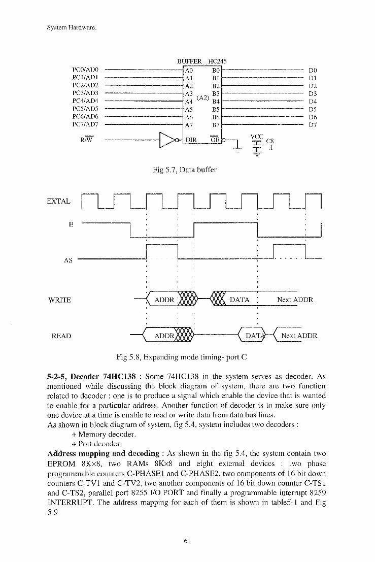
System Hardware.
EXTAL
PeOJADO Pel/AD I Pe2/AD2 Pe3/AD3 Pe4/AD4 Pe5/AD5 Pe6/AD6 Pe7/AD7
RIW
E
BUH"'ER HC245 -AO BO Al Bl A2 B2 A3 (A2) B3 A4 B4 AS B5 A6 B6 A7 B7
{::>o-nrR OE~
Fig 5.7, Data buffer
vee :r: es I .1
DO Dl D2 D3 D4 D5 D6 D7
AS -------~-----~.-__ I _____ L
WRITE -< ADDR ~.,_, ......... _D_A_T_A_-:--__ N_e_x_t _ADDR
READ -( ADDR~,_' -----<( DATH NextADDR
Fig 5.8, Expending mode timing- port C
5-2-5, Decoder 74HC138 : Some 74HC138 in the system serves as decoder. As mentioned while discussing the block diagram of system, there are two function related to decoder : one is to produce a signal which enable the device that is wanted to enable for a particular address. Another function of decoder is to make sure only one device at a time is enable to read or write data from data bus lines. As shown in block diagram of system, fig 5.4, system includes two decoders:
+ Memory decoder. + Port decoder.
Address mapping and decoding : As shown in the fig 5.4, the system contain two EPROM 8Kx8, two RAMs 8Kx8 and eight external devices : two phase programmable counters C-PHASEl and C-PHASE2, two components of 16 bit down counters C-TVl and C-TV2, two another components of 16 bit down counter C-TSl and C-TS2, parallel port 8255 I/0 PORT and finally a programmable interrupt 8259 INTERRUPT. The address mapping for each of them is shown in table5-1 and Fig 5.9
61
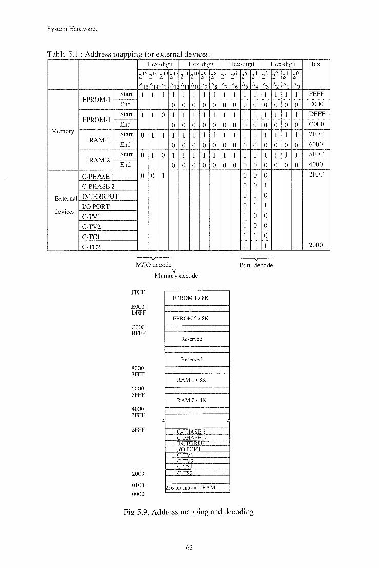
System Hardware.
Table 5.1 : Address mapping for external devices.
EPROM-I
EPROM-I
Memory RAM-1
RAM-2
C-PHASE 1
C-PHASE2
External INTERRPUT
I/0 PORT devices
C-TV1
C-TV2
C-TC1
C-TC2
Hex-digit Hex-digit Hex-digit Hex-digit
215 214 213 212 211 210 29 28 27 26 25 24 23 22 21 20
AL AI AL AI All Ale A9 As A7 A6 As A4 A3 A2 AI Ao
Start 1 1 1 1 1 1 1 1 1 1 1 1 1 1 1 1 - - - - - - - - - - - - - - - -· - -
End 0 0 0 0 0 0 0 0 0 0 0 0 0
Start 1 1 0 1 1 1 1 1 1 1 1 1 1 1 1 1 - - - - - - - - - - - - - - - - - - - -
End 0 0 0 0 0 0 0 0 0 0 0 0 0
Start 0 1 1 1 1 I 1 1 1 1 1 1 1 1 1 1 - - - - - - - - - - - - - - - - - - - - -
End 0 0 0 0 0
Start 0 1 0 1 1 I 1 1 - -
End 0 0 0 0 0
0 0 1
~el Memory decode
FFFF
EOOO DFFF
cooo BFFF
8000 7FFF
6000 5FFF
4000 3FFF
2FFF
2000
0100 0000
EPROM I /SK
EPROM2/8K
Reserved
Reserved
RAM 1 I 8K
RAM2/8K
C-PHASE 1 C-PHASE 2 INTERRUPT I/0 PORT C-TVl ( -TV2 C-TSJ c T"c
~56 bit internal RAM
0
1 - -
0
0 0 0 0
1 1 1 1 - - - - - - - - -
0 0 0 0
0 0 0 - - -
0 0 1 - - -
0 1 0 - - -
0 1 1 - - -
1 0 0 - -
1 0 0 . - - - -
1 1 0 . - - - - -
1 1 1
-y-
Port decode
Fig 5.9, Address mapping and decoding
62
0 0 0
1 1 1 - - - - -
0 0 0
Hex
FFFF - - - - -EOOO
DFFF - - - - -cooo 7FFF
- - - - -
6000
5FFF - - -
4000
2FFF
2000
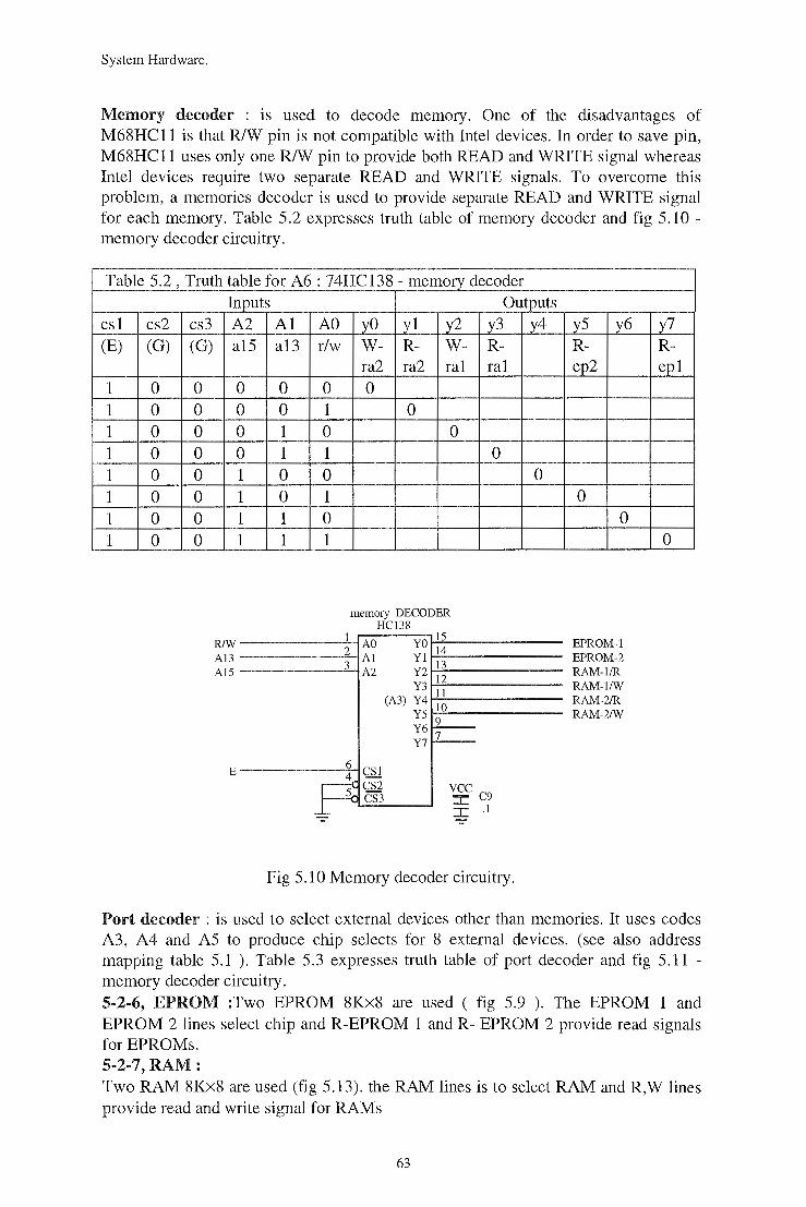
System Hardware.
Memory decoder : is used to decode memory. One of the disadvantages of M68HC11 is that RIW pin is not compatible with Intel devices. In order to save pin, M68HC11 uses only one RIW pin to provide both READ and WRITE signal whereas Intel devices require two separate READ and WRITE signals. To overcome this problem, a memories decoder is used to provide separate READ and WRITE signal for each memory. Table 5.2 expresses truth table of memory decoder and fig 5.10 -memory decoder circuitry.
Table 5.2, Truth table for A6 : 74HC138- memory decoder
csl cs2 cs3 (E) (G) (G)
1 0 0 1 0 0 1 0 0 1 0 0 1 0 0 1 0 0 1 0 0 1 0 0
Inputs A2 a15
0
R/W Al3 Al5
E
0 0 0 1 1 1 1
AI a13
0 0 1 1 0 0 1 1
AO r/w
0 1 0 1 0 1 0 1
1 2 3
yO yl y2 W- R- W-ra2 ra2 ral 0
0 0
memory DECODER HC138
AO YO 15
AI Yl 14
A2 Y2 13 Y3 12
(A3) Y4 ll Y5 10
Y6 9
Y7 7
6 CS!
Outputs y3 y4 R-ral
0 0
4 -pcs2 vee c 9 CS3 :r: .I
Fig 5.10 Memory decoder circuitry.
y5 y6 R-ep2
0 0
EPROM-! EPROM-2 RAM-1/R RAM-1/W RAM-2/R RAM-2/W
y7 R-epl
0
Port decoder : is used to select external devices other than memories. It uses codes A3, A4 and A5 to produce chip selects for 8 external devices. (see also address mapping table 5.1 ). Table 5.3 expresses truth table of port decoder and fig 5.11 -memory decoder circuitry. 5-2-6, EPROM :Two EPROM 8Kx8 are used ( fig 5.9 ). The EPROM 1 and EPROM 2 lines select chip and R-EPROM 1 and R- EPROM 2 provide read signals forEPROMs. 5-2-7, RAM: Two RAM 8Kx8 are used (fig 5.13). the RAM lines is to select RAM and R,W lines provide read and write signal for RAMs
63
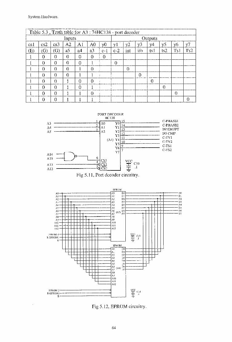
System Hardware.
Table 5.3, Truth table for A3 : 74HC138- port decoder
csl (E) 1 1 1 1 1 1 1 1
cs2 cs3 (G) (G) 0 0 0 0 0 0 0 0
A3 A4 AS
A14 Al5
A13 Al2
0 0 0 0 0 0 0 0
AO AI A2 A3 A4 AS A6 A7 AS A9
AIO All Al2
EPROM-I R-EPROMl
E
EPROM-2 R-EPROM2
E
Inputs A2 a5 0 0 0 0 1 1 1 1
AI AO a4 a3 0 0 0 1 1 0 1 1 0 0 0 1 1 0 1 1
I
yO yl c-1 c-2 0
0
PORT DECODER HC138
1 AO YO 15
2 A1 Yl 14 3 A2 Y2 13
Y3 12
(A4) Y4 1l Y5 10
Y6 9
Y7 7
6 4 CS1
5 CS2 CS3
Outputs y2 y3 y4 int i/o ts 1
0 0
0
'±C ClO I .1 -
Fig 5.11, Port decoder circuitry.
EPROM
AO DO AI Dl A2 D2 A3 D3 A4 D4 AS DS
A6 (A?) D6 A7 D7 AS A9 AlO All Al2
¥cl3 ~.I
EPROM
AO DO Al Dl A2 D2 A3 D3 A4 D4 AS D5
A6 fASn D6 A7 V""' D7
AS A9 AlO All Al2
¥c14 ~.I
Fig 5.12, EPROM circuitry.
64
y5 y6 ts2 Tsl
0 0
C-PHASEJ C-PHASE2 INTERUPT I/0 CHIP C-TV1 C-TV2 C-TS1 C-TS2
DO Dl D2 D3 D4 D5 D6 D7
y7 Ts2
0
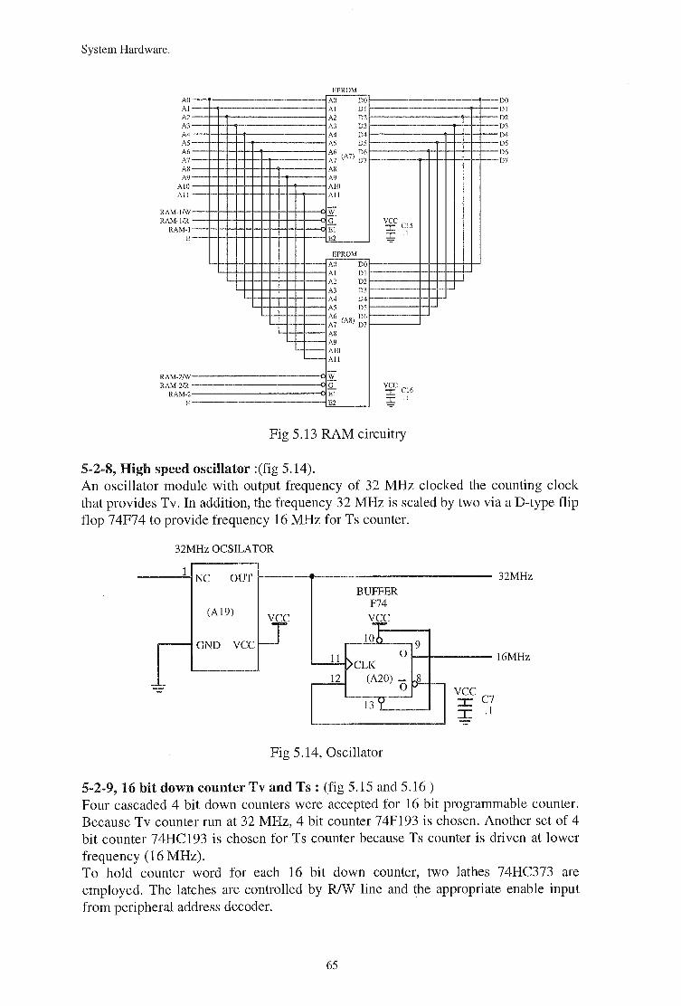
System Hardware.
AO AI A2 A3 A4 A5 A6 A7 AS A9
AlO All
RAM-1/W RAM-1/R
RAM-I E
RAM-2/W RAM-2/R
RAM-2 E
1-'-
EPROM
AO DO AI Dl A2 D2 A3 D3 A4 D4 AS DS
A6 (A7) D6 A7 D7 AR A9 AlO All
-1f_ .Q...
¥c1s El E2 ~ .1
EPROM
AO DO AI Dl A2 D2 A3 D3 A4 D4 AS D5
A6 (AS) D6 A7 D7 AS A9 AlO All
-1f_ .Q...
¥cJ6 El E2 ~.I
Fig 5.13 RAM circuitry
5-2-8, High speed oscillator :(fig 5.14).
DO Dl D2 D3 D4 DS D6 D7
An oscillator module with output frequency of 32 MHz clocked the counting clock that provides Tv. In addition, the frequency 32 MHz is scaled by two via aD-type flip flop 74F74 to provide frequency 16 MHz forTs counter.
32MHz OeSILATOR
----'~Ne OUT 1-----+------------ 32MHz
(A19)
GND vee
BUFFER F74
vee
.---'1""0......_ _ _, 9
Fig 5.14, Oscillator
0 1-+----- 16MHz
vee :X: e7 I .1
5-2-9, 16 bit down counter Tv and Ts: (fig 5.15 and 5.16) Four cascaded 4 bit down counters were accepted for 16 bit programmable counter. Because Tv counter run at 32 MHz, 4 bit counter 74F193 is chosen. Another set of 4 bit counter 74HC193 is chosen forTs counter because Ts counter is driven at lower frequency (16 MHz). To hold counter word for each 16 bit down counter, two lathes 74HC373 are employed. The latches are controlled by R/W line and the appropriate enable input from peripheral address decoder.
65
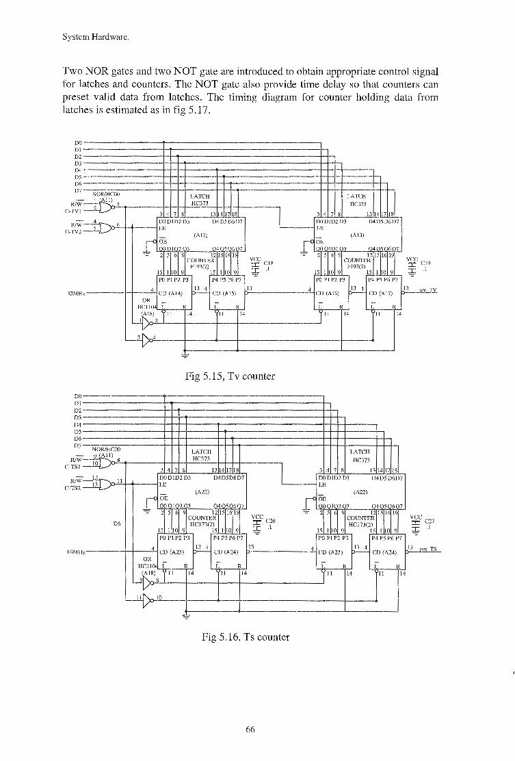
System Hardware.
Two NOR gates and two NOT gate are introduced to obtain appropriate control signal for latches and counters. The NOT gate also provide time delay so that counters can preset valid data from latches. The timing diagram for counter holding data from latches is estimated as in fig 5.17.
DO Dl D2 D3 D4 D5 D6 D7
NORJHCOO
R/W C-TV!
-=±D) ~
3
R!W C-TV2
32MH
DO D1 D2 D3 D4 D5 D6 D7
R!W C-TSI
z
4_,... 6
5] -.-
NORJHCOO 9JA.ll) 10] 8
--,;...-
-=tiD 3 ~
R!W C-TS2
11
D6
16M! Iz
LATCH HC373
3 4 7 8 13 14 17 18 I DOD!D2D3 D4D5D6D7 LE
(A12)
.rOE lcoc 1c2 3 (4(5 6 7 - 2 5 6 9 1215 16 19
COUNTER '§fc1s 1'193(2)
15 1 10 9 15 1 10 9 ~ .1
PO P1P2 P3 P4 P5 P6 P7
4 ~ 13 CD (A14) CD (A15)
OR HCllO L' R L' R
~8) 11 14 11 14 2
44
Fig 5.15, Tv counter
LATCH HC373
I 3 4 7 8 I3I4 1718 DODID2D3 D4D5D6D7 LE
(A22)
rOE LQO( IC2 3 Q4J:5J: 6 7
- 2 5 6 9 I215 I6I
'§fc26 COUNTER HCI73(2)
I5 I IO 9 15 I 10 9 :::r: .1
PO PI P2 P3 P4 P5 P6 P7
4 CD (A23) ~ 13
CD (A24) OR
HC!IO L' R L' R
4>8) 11 I4 11 I4
8
.. r-.. 10 ll ~
Fig 5.16, Ts counter
66
LATCH
HC373
3 4 7 8 13 14 17 18 DOD1D2D3 D4D5D6D7 LE
(Al3)
.rOE I CO( 1( 2 3 C40 6 7 -:::- 2 5 6 9 1215 16 19
COUNTER '§fc19 F193(2)
15 1 10 9 15 1 10 9 :::r: .1
PO PI P2 P3 P4 P5 P6 P7
4 ~ 13 pre TV CD (A16) CD (Al7)
L' R L' R 11 14 11 14
LATCH
HC373
3 4 7 8 I3I4 I7 18 DOD!D2D3 D4D5D6D7 LE
(A22)
rOE QOJ; !i 2 3 _Q4J: 5_( 6 7
-::- 2 5 6 9 COUNTE~r I619 ~c c27 HCI73(2)
15 I 10 9 I5 I 10 9 :::r: .1
PO PI P2 P3 P4 P5 P6 P7
4 p 13 Jrc TS CD (A23) CD (A24)
L' R L R 1I 14 11 I4
~
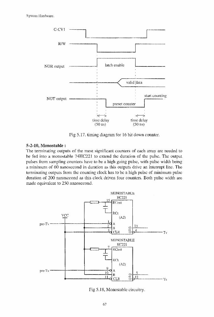
System Hardware.
C-CVl
R/W
NOR output
NOT output
5-2-10, Monostable:
latch enable
------..!...-----<( valid :data
' ' '~
time delay (50 ns)
start counting
' preset countet: I ' ' ,-<~
time delay (50 ns)
Fig 5.17, timing diagram for 16 bit down counter.
The terminating outputs of the most significant counters of each array are needed to be fed into a monostable 74HC221 to extend the duration of the pulse. The output pulses from sampling counters have to be a high going pulse, with pulse width being a minimum of 60 nanosecond in duration as this outputs drive an interrupt line. The terminating outputs from the counting clock has to be a high pulse of minimum pulse duration of 200 nanosecond as this clock driven four counters. Both pulse width are made equivalent to 250 nanosecond.
vee --pre-Tv
pre-Ts
MONOSTABLE He221
...--. 15 - j_ Reext
L_Ret (A2)
1 A
2 B 0
3 -eLR 0
13 4
MONOSTABLE He221
..--.. 7 - i_ RCext
Ret (A2)
9 A
10 5 11
B 0 ~ eLR 0 12
Fig 5.18, Monostable circuitry.
67
Tv
Ts
System Hardware.
5-2-11, Programmable 8 bit counters: Four programmable 8 bit counter are required : three are required to generate the pulse widths and delay times for three phase outputs, one is to trace the carrier period during asynchronous mode. Two INTEL 82C53 Programmable counter are employed to satisfy these system requirements. Each chip contains three independently operating 16 bit counters which can be programmed to operate as 8 bit counters. Three pulse widths counters are situates on a single 82C53 while Tsa counter occupy the other chip as shown in fig 5.19.
DO D1 D2 D3 D4 D5 D6 D7
C-PHASE 1 R w
AO Al
Tv
C-PHASE R w
AO A1
~
PROGRAMMABLE COUNTER vee 8254 -r-
DO OUTO PHASE A Dl GATED D2 CLKQ D3 D4 D5 OUTO PHASEB D6 GATEO D7 CLK~
-cs RD WR OUTO PHASEC
AO GATEO
CLK«l A1 vee :r:: C7
I .1 -
PROGRAMMABLE COUNTER 8254
DO OUTO Tsa Dl GATEO D2 CLK~
D3 D4 D5 OUTO D6 GATEO D7 CLK«! -cs RD WR OUTO vee vee c AO
GATEO :r:: C7 :J:+ 7
A1 CLK«! I .1 ~- 4.7uF
- -
Fig 5.19 , Configuration of the 8 bit counter
All phase counter have been incorporated in the design assuming they are to operate as time-out counters, that is the OUT pin of each counter goes high on the termination of the counter are remains high until a new count is loaded. This is referred to as MODEO operation. All counters on the other programmable counter must operate in MODE 2 where the OUT pin outputs a square wave with frequency equal to the driving clock divided by the count issued to the counter. These modes of operation must be initialised by writing to the control register of each counter. The OUT pins of the three phase counters and the Tsa counter drive are used to issue interrupt requests to the CPU.
68
System Hardware.
5-2-12, Interrupt: A maximum of five counters are required to issue interrupts to the CPU, which occurs during three phase, asynchronous, uniform sampling operation. These include the sampling clock Ts, the carrier clock Tv and three phase counters. The programmable interrupt controller 8259 can provide up to eight interrupt inputs with programmable priority management and is directly interfaceable with the CPU. As only five input are required, the remaining three inputs are masked by software. The programmer can specify the five most significant bit of this pointer. During initialisation, the controller inserts the three least significant bits automatically depending on the input request interrupt. Therefore, four address location must contain the new instruction pointer and code segment register relating to the start of the service routine.
DO D1 D2 D3 D4 DS D6 D7
IRQ INTERUPT
R w
AO
5-2-13, Interfacing circuitry :
11 10 9 8 7
6 5 4
17 26 1 3 2
27
INTERRUPT 8259
DO IRl D1 IRl D2 IR D3 IR D4 IR DS TR' D6 IRt D7 TR~
vee INT TNTA LJ cs SP/E RD CAS WR CAS AO CAS
Fig 5.20, Interrupt
Tc Tsa phase a phase b phase c
The modulator is required to send logic signal to the power inverter via an isolation and driver circuit in order to turn the switching on/off to produce the correct PWM output. + Parallel interfacing port : the modulator utilise a programmable parallel interface (PPI) 8255 to provide interface. The PPI has three independently addressed 8 bit ports which can be configured to be output or input ports by software. The 8255 is to be configured as an all output port which can achieve by sending a control byte to the control register. Only three output to the PPI are required because the other signals, there exists six switching elements on the inverter, are simply complement of complement sign. This is because the series pairs of MOSFET's can not turned on simultaneously as a short circuit will occur causing damage to the MOSFET's. + Synchronising circuit : To prevent any time error, The output of parallel port are put through three D-type synchronising flip flop 74F74. The three flip-flop are clocked by the counting clock ts. + Isolation : provide protection to the digital circuit of the modulator if any power
MOSFET becomes damaged.
69
System Hardware.
Tv -------------------------------------, vee
PARALELLPORT 8255A
D0-------"'"'-1 DJ-------"'-"'-1 D2------"""'"-lD2
D3 D3 D4 D4 DS DS D6 D6 D7 D7
l/0 POR1 26 es
RESET----~-; RESET w----~-q
RD
BUFFER F74
+---t--""-3 1>eLK (A40-1)
AO ------lAO Al AI r-~e~D~~o~5------SW5
Fig 5.21, Output port.
OR-GATE 74F06
~ +5v ' - (A?_?)_ -: R /270
1~2 &~[451 :=J] SW1 GATE-I
vee R 1270 +Sv
T R /270
5~6 ~ ;i~tZJI :=J] SW2 GATE-2
~ +Sv
I R /270
:]]~< ;i~[ZJI ::::J SWI GATE-3
~ +Sv
I R /270
:s~ ;i~tZJI ::::J SW1 GATE-4
+5v
~ I R /270
2~8 ~~~I ::::J SWI GATE-5
~ +5v
£j~[451 I R /270
:11~12: ::::J SW1 GATE-6
Fig 5.22 Isolation circuit.
70
System Hardware.
5-3, Current and speed sensor.
5-3-1, Current sensor. The project employs a three phase current detection available in the power lab. However, some aspects related to current detection should be included. Normally, the motor current is detected by Hall effect current transducer. A device supplied by Honeywell Microswitch can be selected. This kind of device has three pins which can be connected as in [19]. The output from transducer is a voltage which is from 25% to 75% of the voltage supply and can be calculated by the following formula:
V =V +(0.0364xNxi) VccxK output offset - I X 12
g
(5.8)
Where: voffset = output voltage at zero current. N =No. of the current carrying conductor passing. I = magnitude of current in the current carrying conductor. Ig = gap cut in the flux collector. Vee =voltage supply. K =constant depending on Vee.
The maximum motor current is 15 A. From eq (5.8), in order to obtain output voltage range 5V to 6V de, 4 turn around the flux collector are required.
5-3-2, Speed sensor. Shaft encoder is used in this project to detect motor speed. Fig 5.23 shows simplified configuration of motor shaft encoder.
M68HC11 microcontroller
motor toothed wheel
D© It:=}-~__. sensor
Fig 5.23, Simplified configuration of motor shaft encoder.
The principle of motor shaft encoder can be explained as follow : a toothed wheel is mounted on the motor shaft and an opto-switch generates pulse as motor shaft rotates. On the rising edge of each pulse, the microcontroller reads its free-running internal 16 bit counter- the input clock to this counter is driven from the primary microcontroller clock at 2 MHz. The microcontroller then generates a stream of 16 bit binary words, each word corresponding to the start of a pulse from the toothed wheel. Pulse period
71
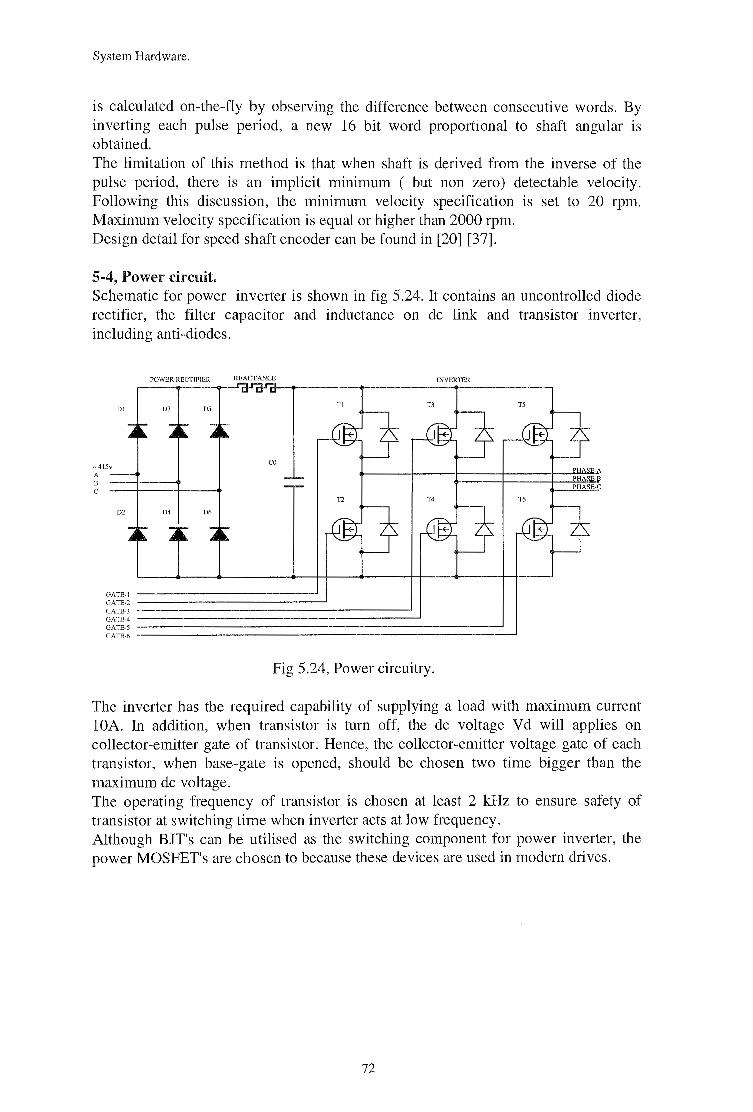
System Hardware.
is calculated on-the-fly by observing the difference between consecutive words. By inverting each pulse period, a new 16 bit word proportional to shaft angular is obtained. The limitation of this method is that when shaft is derived from the inverse of the pulse period, there is an implicit minimum ( but non zero) detectable velocity. Following this discussion, the minimum velocity specification is set to 20 rpm. Maximum velocity specification is equal or higher than 2000 rpm. Design detail for speed shaft encoder can be found in [20] [37].
5-4, Power circuit. Schematic for power inverter is shown in fig 5.24. It contains an uncontrolled diode rectifier, the filter capacitor and inductance on de link and transistor inverter, including anti-diodes.
-415v A B c
Dl
POWER RECTIFIER REACTANCE
03 05
co
04 06
GATE-! ----------------' GATE-2 --------------l
Tl
GATE-3 =================='-J GATE-4
INVERTER
T3
GATE-5 =======================::__] GATE-6
Fig 5.24, Power circuitry.
T5
The inverter has the required capability of supplying a load with maximum current 1 OA. In addition, when transistor is turn off, the de voltage V d will applies on collector-emitter gate of transistor. Hence, the collector-emitter voltage gate of each transistor, when base-gate is opened, should be chosen two time bigger than the maximum de voltage. The operating frequency of transistor is chosen at least 2 kHz to ensure safety of transistor at switching time when inverter acts at low frequency. Although BIT's can be utilised as the switching component for power inverter, the power MOSFET's are chosen to because these devices are used in modern drives.
72
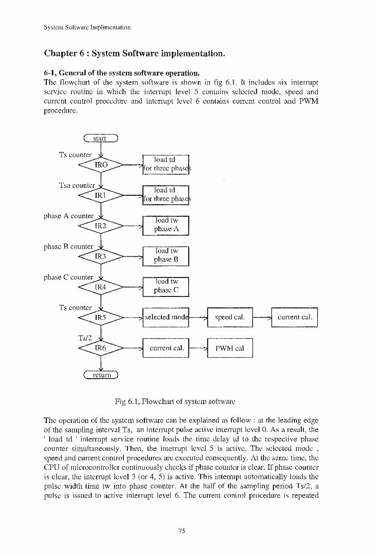
System Software Implimentation
Chapter 6 : System Software implementation.
6-1, General of the system software operation. The flowchart of the system software is shown in fig 6.1. It includes six interrupt service routine in which the interrupt level 5 contains selected mode, speed and current control procedure and interrupt level 6 contains current control and PWM procedure.
load td or three phas
load td for three phas
load tw phase A
load tw phase B
load tw phase C
current cal.
speed cal.
PWM cal
Fig 6.1, Flowchart of system software
current cal.
The operation of the system software can be explained as follow : at the leading edge of the sampling interval Ts, an interrupt pulse active interrupt level 0. As a result, the 1 load td 1 interrupt service routine loads the time delay td to the respective phase counter simultaneously. Then, the interrupt level 5 is active. The selected mode , speed and current control procedures are executed consequently. At the same time, the CPU of microcontroller continuously checks if phase counter is clear. If phase counter is clear, the interrupt level 3 (or 4, 5) is active. This interrupt automatically loads the pulse width time tw into phase counter. At the half of the sampling period Ts/2, a pulse is issued to active interrupt level 6. The current control procedure is repeated
75
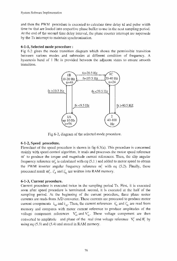
System Software Implimentation
and then the PWM procedure is executed to calculate time delay td and pulse width time tw that are loaded into respective phase buffer to use in the next sampling period. At the end of the second time delay interval, the phase counter interrupt are supersede by the Ts interrupt to maintain synchronisation.
6-1-1, Selected mode procedure : Fig 6.2 gives the mode transition diagram which shows the permissible transition between various modes and submodes at different condition of frequency. A hysteresis band of 1 Hz is provided between the adjacent states to ensure smooth transition.
fs>20.5 Hz
fs<19.5 Hz
fs > 10.5 Hz fs <39.5 Hz
fs <9.5 Hz fs >40.5 HZ
Fig 6-2, diagram of the selected mode procedure.
6-1-2, Speed procedure. Flowchart of the speed procedure is shown in fig 6.3(a). This procedure is concerned mainly with speed control algorithm. It reads and processes the motor speed reference cor to produce the torque and magnitude current references. Then, the slip angular frequency reference co~, is calculated with eq (5.1 ) and added to motor speed to obtain the PWM inverter angular frequency reference CD~ with eq (5.2). Finally, these processed result ro;·, i;·ct and i~q are written into RAM memory.
6-1-3, Current procedure. Current procedure is executed twice in the sampling period Ts. First, it is executed soon after speed procedure is terminated. second, it is executed at the half of the sampling period. At the beginning of the current procedure, three phase motor currents are reads from AID converter. These currents are processed to produce motor current components i," and i,~. Then, the current references i~" and i~~ are read from
..1.. J.U H.. . H.l ''i
memory and compares with motor current reference to produce amplitudes of the voltage component references V1
1~ and V1~ . These voltage component are then
converted to amplitude and phase of the real time voltage reference Vt and 8~ by using eq (5.3) and (5.4) and stored in RAM memory.
76
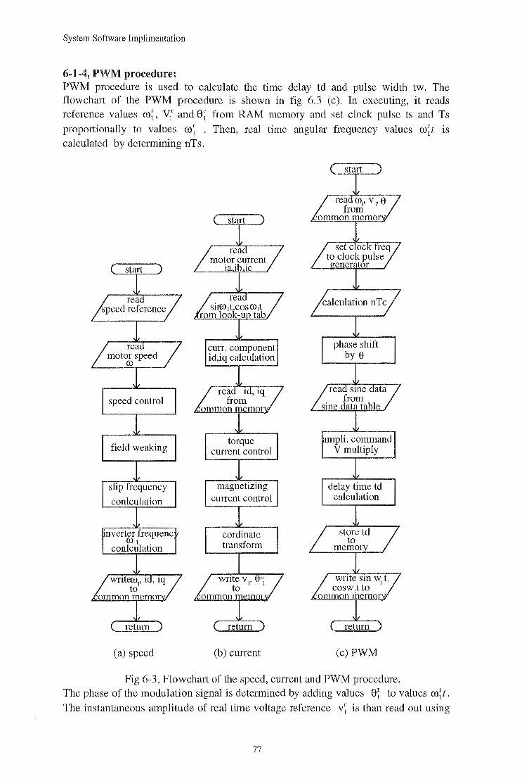
System Software Implimentation
6-1-4, PWM procedure: PWM procedure is used to calculate the time delay td and pulse width tw. The flowchart of the PWM procedure is shown in fig 6.3 (c). In executing, it reads reference values ro;, V/ and e;· from RAM memory and set clock pulse ts and Ts proportionally to values ro; . Then, real time angular frequency values ro;t is calculated by determining nTs.
(a) speed (b) current (c) PWM
Fig 6-3, Flowchart of the speed, current and PWM procedure. The phase of the modulation signal is determined by adding values e; to values ro;·t. The instantaneous amplitude of real time voltage reference v;· is than read out using
77
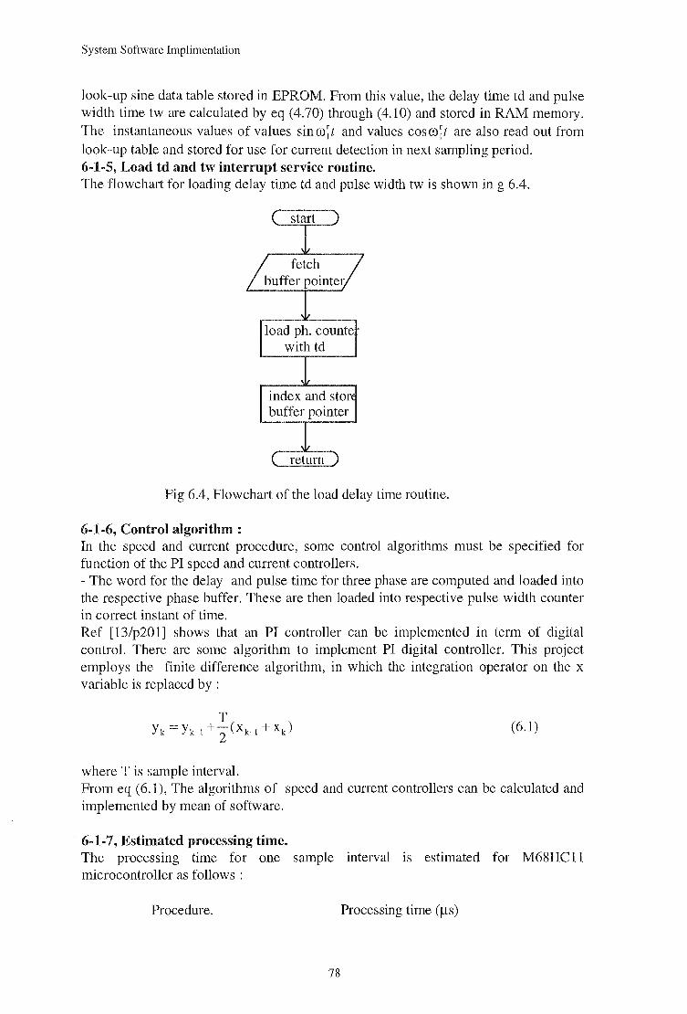
System Software Irnplirnentation
look-up sine data table stored in EPROM. From this value, the delay time td and pulse width time tw are calculated by eq (4.70) through (4.10) and stored in RAM memory. The instantaneous values of values sin ffi~ t and values cos ffi~ t are also read out from look-up table and stored for use for current detection in next sampling period. 6-1-5, Load td and tw interrupt service routine. The flowchart for loading delay time td and pulse width tw is shown in g 6.4.
load ph. counte with td
Fig 6.4, Flowchart of the load delay time routine.
6-1-6, Control algorithm : In the speed and current procedure, some control algorithms must be specified for function of the PI speed and current controllers. - The word for the delay and pulse time for three phase are computed and loaded into the respective phase buffer. These are then loaded into respective pulse width counter in correct instant of time. Ref [13/p201] shows that an PI controller can be implemented in term of digital control. There are some algorithm to implement PI digital controller. This project employs the finite difference algorithm, in which the integration operator on the x variable is replaced by :
(6.1)
where T is sample interval. From eq ( 6.1 ), The algorithms of speed and current controllers can be calculated and implemented by mean of software.
6-1-7, Estimated processing time. The processing time for one sample interval rs estimated for M68HC11 microcontroller as follows :
Procedure. Processing time (~s)
78

System Software Implimentation
Mode Load time Speed current PWM
50 50 150 250x2 200
It shows that total processing time is estimated lOOOf!s, or 1ms. Therefore, sample frequency, also carrier frequency, is limited below 1kHz as mentioned in chapter 3.
6-2, Software implementation in C++ System software can be implemented in either assembly or high level languages such as C or pascal. However, high level language programs are much more convenience in comparing with assembly language:
* They are more likely to be self-documenting. * The structure of the program can be made to reflect the structure of the original problem. * Meaningful names can be chosen for variables and subprograms. * The solution of the problem need not be obscured by the level of detail necessary in an assembler program.
From this point of view, high level languages are initial choice. Regarding that compiler for pascal is not available in lab, the C++ language is finally chosen to develop system software in this project. All function of the PMW-IM drive system mentioned in previous chapters can be written in C++ language using Borland text editor. C++ program is then converted into an OBJ file by using HI-TECH compiler and subsequently, this file produces appropriate files contains binary code and the hexadecimal code. The hexadecimal code is required to ensure the conversion from mnemonics to machine code is correct.
6-2-1, Direct access of peripheral devices: It is important to know the way a certain external device is accessed using C++ because each external device must be accessed, initialised and controlled when program is executed. C++ provides two special functions, declared in header file <conio.h>, for accessing external devices [24]:
int input (int io_ port) int output (int io_ port)
/*read a byte from io_ port *I /*write a byte to io_ port*/
Here, ' io_ port' is defined as address of the external device including addresses of registers as a part of that external device. When called, input function return the byte read from the specified external device and output function write a byte to the device. By using these function, data or status information of a certain device in IM control system, such as Ts and ts counter, parallel port, etc, can be passed between microcontroller and external devices via data bus. The addresses of each device can be found in the address mapping table 5.2, chapter 5.
6-2-2, Interrupt programming : As shown in the fig 6.1, the system software contains 6 hardware interrupt. The service routines for each interrupt are explained in the previous section. From view
79
System Software Implimentation
point of software implementation, these service routine must be first set up in the form of a interrupt procedure. This can be done in C++ by define [24]:
void interrupt (far int_ procedure (void)) {
/* interrupt procedure body */ }
The key word ' interrupt' tells the compiler that this is an interrupt service routine, The compiler will generate the appropriate entry and exit sequences including saving and restoring registers ( in processor ) and terminating the procedure with an IRET (interrupt return) instruction. Next, the interrupt service routine is set to interrupt level of interrupt controller. C++ provides function setvect to do this job.
void setvect (int int_ number, void interrupt ( * int_procedure)( ))
This function loads the interrupt level 'int-number, for the interrupt service routine int_procedure via its address. All interrupt service routine of PWM-IM system software such as time delay calculation, speed and current procedure, etc, are written by using the functions explained above.
6-2-3, Initialisation for external devices. As mentioned, all external devices must be initialised before main program is
executed. Normally, each device interface contains a number of register which can pass data and status/control information between the program running in the processor and that device. Therefore, in order to initialise a device, its structure must be studied from data sheet. Then, mode word must be specified to each register of the device. finally, the concerning device can be initialise by transmitting a specified byte to its registers by mean of software. In the software implementation of PWM-IM drive system, some care must be taken in initialisation for external devices : +All three port of the parallel interface are declared as output ports. Each output port must be kept low during the initialisation stage. +The phase counter is operated in MODEO while Ts counter is operated in MODE3. + The interrupt controller is declared to be used in M6800 system. The interrupt input is unmasked. The interrupt vector table must be written in system RAM. + The communication interface must be reset. Once initialisation is completed, the CPU will monitor the communication status register until the speed command is issued. On receiving data, the CPU loads the relevant counts to the system counter, sets the output logic ad the unmasks the interrupt enable flags to allow the CPU to accept interrupts. The CPU the simply service the interrupts of the system as they occur.
80

System Software Implimentation
7-2-4, Communication programming. The function of the communication programming is to send motor speed reference from host computer to the M68HC11 microcontroller and/or receives system status if drive is used in data acquisition system. The communication subject is somewhat difficult to approach and beyond the scop of this project. This section only discussion general ideas of system communication, focus on communication programming in C++. However, detail studies can be found in ref [22], [23]. In order to transfer over long distance, data between host computer and microcontroller is transmitted in serial via RS-232 interface. Three terms often encountered on serial data communication are simplex, haft-duplex and full-duplex, that are the way data is transmitted. Some the other terms are related to structure of data to be sent: start and stop bit, parity bit and baud rate [22]. The project employs the simplex transmission in which data is transmitted only in one direction. However, half I full duplex transmission can be used if the drive is developed to be used in data acquisition system or CIM system. To initialise the serial port (port D) of M68HC11 microcontroller, a mode word and then command word are sent to the addresses of status/control registers of port D. By such a way, number of start bit, stop bit, parity bit and baud rate are set to serial port of microcontroller. A procedure is then written for microcontroller to receive data from host computer, depending on status of the clear-to-send (CTS) pin. The same way can be applied to host computer. However, the project employs an another method in which the serial port COM of computer is accessed, initialised and controlled via some special function of ROM BIOS. This method shows a simplification in programming and hence is discussed here. The ROM BIOS provide four functions via interrupt type 14H for controlling serial ports (COMO: to COM3:). In all cases, register ah of CPU contains function numbers ( 0 to 3 ) and register dx contains the serial port numbers ( 0 to 3 ). A brief description of each function is presented as following : Function 0 : is used to initialise serial port. The data word format is specify m register al of CPU.
bit 1,2 word length of processing data : 10 for 7 bits and 11 for 8 bits. bit 2 number of stop bit : 0 for one stop bit and 1 for two stop bit. bit 3,4 parity bit: 00 non, 01 odd, 10 non, 11 even. bit 5,6,7 baud rate : from 000 for 110 baud to 111 for 9600 baud.
Function 1 : transmits data. Data to transmit is stored in al register. On returned, bit 7 of ah will be set if an error occurs and the remainder of ah contains line status. Function 2 : receivers data. When called, this function waits for a character to be received. The character is then transmitted into al register. Bit 7 of ah indicates if any error occurs and bit 1 ,2,3,4 indicate the line status. Function 3 : reads serial port status. It returns the values of the line status in ah register and modem status in al register. In order to access ROM BIOS function for serial communication, C++ provide function int86. When int86 function is called, information is passed to 16 bit processor register ax,bx,cx,dx,si and di or their byte equivalent. In Turbo C++, the function prototype of int86 is declared in header file < dos.h > thus :
int int86 ( int int_number, Union REGS * in_register, Union REGS *out_register );
81

System Software Implimentation
Where: int_number is the interrupt type to invoke the required MS-DOS functions. int_register is the value of the CPU register to be passed to MS-DOS. out_register is the value of the CPU registers as returned by MS-DOS.
The declaration of Union REGS is of the form: I* Intel8086 family word register ( 16 bit), cflag is the carry flag *I
Struct WORD_REGS {Unsigned int ax,bx,cx,dx,si,di,cflag }; I* Intel 8086 family byte registers (8 bit) *I
Struct BYTE_REGS { Unsigned char al,ah,bl,bh,cl,ch.dl,dh}; I* Intel 8086 general purpose registers : overlap word and byte registers *I
Union REGS { Struct WORD_REGS I* Word registers *I Struct BYTE_REGS I* Byte register *I
Using variables of type Union REGS, a CPU register may be accessed as a 16 bit word or a pair of 8 bit byte. By accessing serial port via BIOS functions shown above, one can write program to transmit and receive data from host computer. An example to initialise serial port COM: of the host computer is given in fig 6-6.
I* Procedure to initialise 8250 port number" io_port" with 8 data bit, no parity, one stop bit and 9600 baud. *I void rs_initialise ( const int io_port ) {
}
Union REGS register ;
register.h.ah = 0 ; register.h.al = Oxe3 ; register.x.dx =io_port ;
I* variable to hold 8086 register *I
I* initialize function 0 *I I* set data bit, parity bit, stop bit, baud *I I* specify port number *I
int86 ( Ox14, & register, & register); I* call interrupt type 14H *I
Fig 6.6, Procedure to initialise io_port
There are some advantages of using ROM BIOS functions. First, they may save programming efforts and space in the program file. Second, they make program more compatible with other DOS machine. Finally, programs using DOS and BIOS functions exclusively could be compatible with future versions of the PC.
82
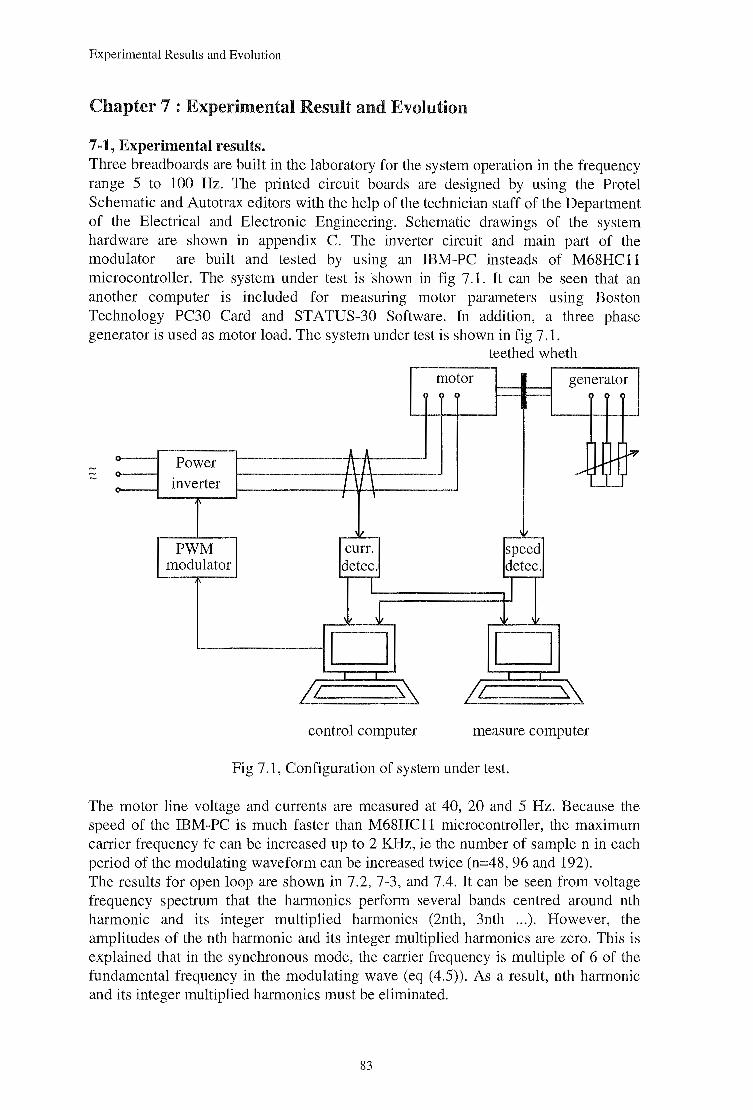
Experimental Results and Evolution
Chapter 7 : Experimental Result and Evolution
7-1, Experimental results. Three breadboards are built in the laboratory for the system operation in the frequency range 5 to 100 Hz. The printed circuit boards are designed by using the Protei Schematic and Autotrax editors with the help of the technician staff of the Department of the Electrical and Electronic Engineering. Schematic drawings of the system hardware are shown in appendix C. The inverter circuit and main part of the modulator are built and tested by using an IBM-PC insteads of M68HC11 microcontroller. The system under test is shown in fig 7 .1. It can be seen that an another computer is included for measuring motor parameters using Boston Technology PC30 Card and ST A TUS-30 Software. In addition, a three phase generator is used as motor load. The system under test is shown in fig 7 .1.
teethed wheth
motor generator
A A JBtt Power 1\ 1\ inverter I \
I I
PWM curr. speed modulator detec. detec.
I I ! !
D D L! ~\ LL ~\
control computer measure computer
Fig 7.1, Configuration of system under test.
The motor line voltage and currents are measured at 40, 20 and 5 Hz. Because the speed of the IBM-PC is much faster than M68HC11 microcontroller, the maximum carrier frequency fc can be increased up to 2 KHz, ie the number of sample n in each period of the modulating waveform can be increased twice (n=48, 96 and 192). The results for open loop are shown in 7.2, 7-3, and 7.4. It can be seen from voltage frequency spectrum that the harmonics perform several bands centred around nth harmonic and its integer multiplied harmonics (2nth, 3nth ... ). However, the amplitudes of the nth harmonic and its integer multiplied harmonics are zero. This is explained that in the synchronous mode, the carrier frequency is multiple of 6 of the fundamental frequency in the modulating wave (eq (4.5)). As a result, nth harmonic and its integer multiplied harmonics must be eliminated.
83

Experimental Results and Evolution
From this point of view, the harmonic with highest amplitude must occur around nth, 2nth, 3nth and so on. That are 48th, 96th, ... harmonics when system operates in the synchronous mode. The current harmonics are much smaller than that of the voltage harmonics because of the act as low-pass filter of the motor magnetising reactance The closed loop has not been tested. However, a problem could be arisen. That is the closed loop processing time seems to be longer than estimated. In such a case, the maximum carrier frequency must be reduced, or some control procedure must be written in assembly language to reduce processing time, or M68HC11 must be replaced by another microcontroller with faster speed.
84
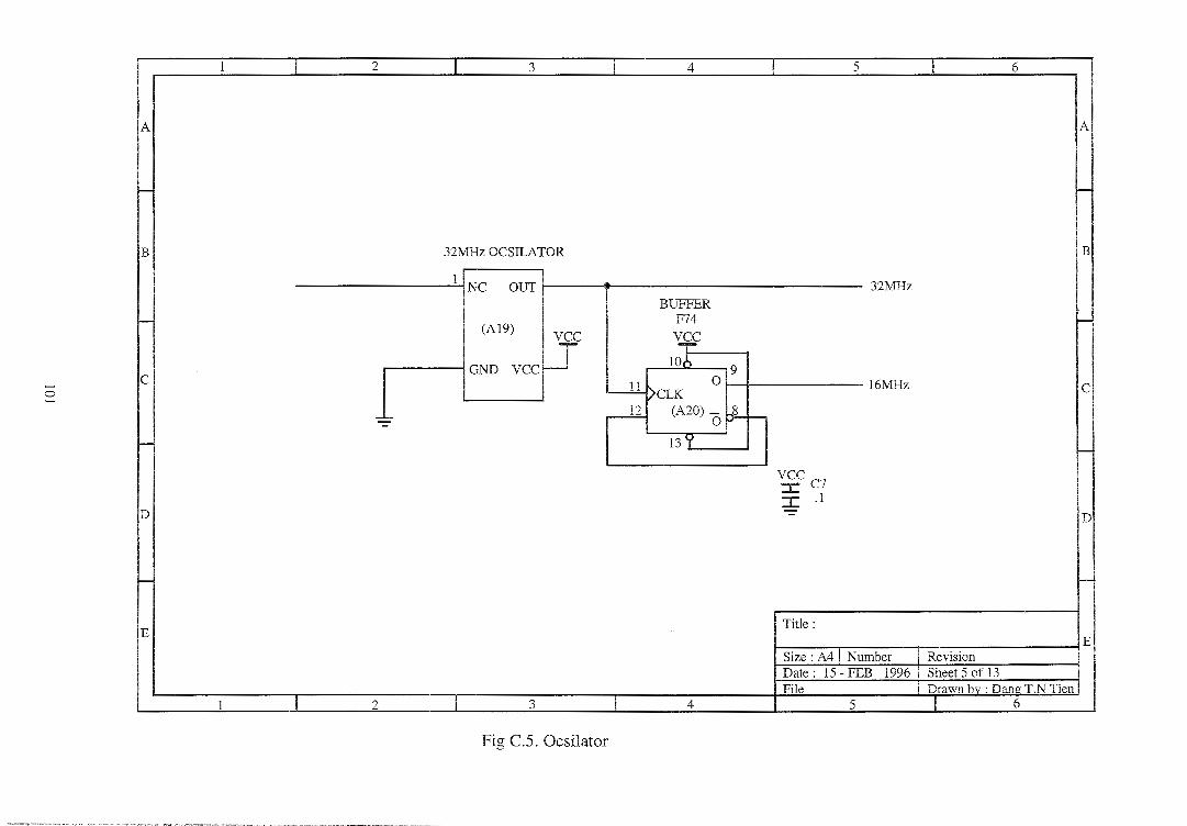
,__.. 0
A
-
B
-
e
'--
D
-
E
1 I 2
-==
1 I 2
I 3 I 4
32MHz OeSILATOR
1 Ne OUT
BUFFER F74
(A19) _y ¥ GND vee
lOb
~ \eLK 0
~ (A20)-0
13Y
I 3 I 4
Fig C.5. Ocsilator
5 I 6
A
,__
B
32MHz I
I--
9 16MHz e
pL - I
~ ±ee7 I .1 - D
-
Title: E
Size : A4 I Number Revision Date: 15- FEB 1996 Sheet 5 of 13 File Drawn by : Dano- T.N Tien
5 I 6
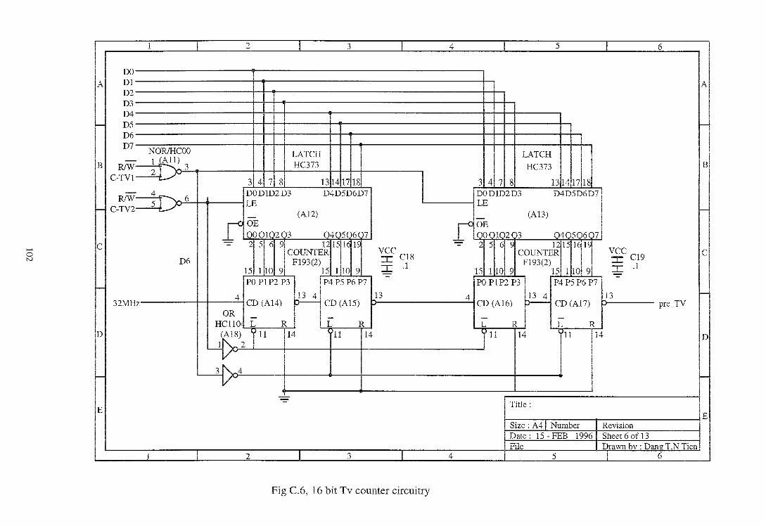
..... 0 N
A
1-
B
DO D1 D2
1 2 I 3 I 4 5
D3 J rn 1 m 1 1 ll D6 D?-N-O-B--~-C-0-0---
LATCH HC373 -~~ll) 1111 c-~ ----1..L>
3
l 31417~ 81 13141718 I 31 41 71 8
LATCH
HC373
13114117118 DOD1D2D3 D4D5D6D7
I 6
A
1-
B
R/W~>6 I t IDOD1D2D3 D4D5D6D7 1--1 C-TV2--4 LE
(Al2) '-------1 LE
_ (A13) 1-
151 111011 91
c vee ::C C18 I .1
vee ::C C19 I .1
D6 c
I J 13 4 D CD(Al7) b---- pre_TV
I P4 P5 P6 P7
13 1-
PO P1P2 P3
4 113 4 32MHz--,---+--+------''-l CD (Al4) p:.::..-.:. 13
CD (Al5) 1-
L R L R L R D 911 114 9u 114 9u 114 D
1- ~4 I l I 1-
.....1-
E Title:
I Size : A41 Number I Revision IE Date: 15- FEB 1996 I Sheet 6 of 13 File I Drawn bv : Dane: T.N Tien
1 2 I 3 I 4 5 ! 6
Fig C.6, 16 bit Tv counter circuitry
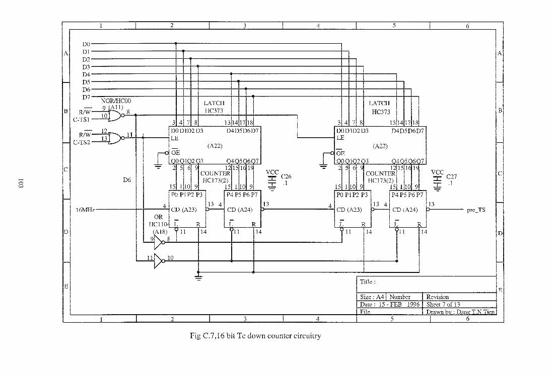
1 2 I 3 I 4 5 I 6
DO
A D1 A D2 D3 D4
I- D5 i--
D6 D7
NORJHCOO LATCH LATCH B -~1) HC373 HC373 B R1W ~, 8
C-TS1 10 .. ~ 3 4 7 8 13 14 17 18 3 4 7 8 13 14 17 18 R/W±, 11 DOD1D2D3 D4D5D6D7 DOD1D2D3 D4D5D6D7
C-TS2 13 rv
LE LE - (A22) (A22) -
-
-0 w
rOE rOE i00(1(2( 3 04(5(6( 7 ooc 1(2( 3 04(5(6( 7
c -=- 2 5 6 9 l:L15 H IS
~CC26 -=- 2 5 6 9 12 15 H 15 vee COUNTER COUNTER c
D6 HC173(2) HC173(2) :c C27
15 110 9 15 1 10 9 :::c .1 15 110 9 15 110 9 :::c .1
PO P1P2 P3 P4P5 P6 P7 PO P1P2 P3 P4 P5 P6 P7 !-
4 ~ 13 4 ~ 13 -16MHz CD (A23) CD (A24) CD (A23) CD (A24) pre_TS
OR - - - -HCllO L R L R L R L R
D ~8) 11 14 11 14 11 14 11 14 D ._28
v I- ~10 i-
-==-- Title : E
E Size : A41 Number Revision Date: 15- FEB 1996 Sheet 7 of 13 File Drawn by : Dam,. T.N Tien
1 2 I 3 I 4 5 I 6
Fig C.7,16 bit Tc down counter circuitry
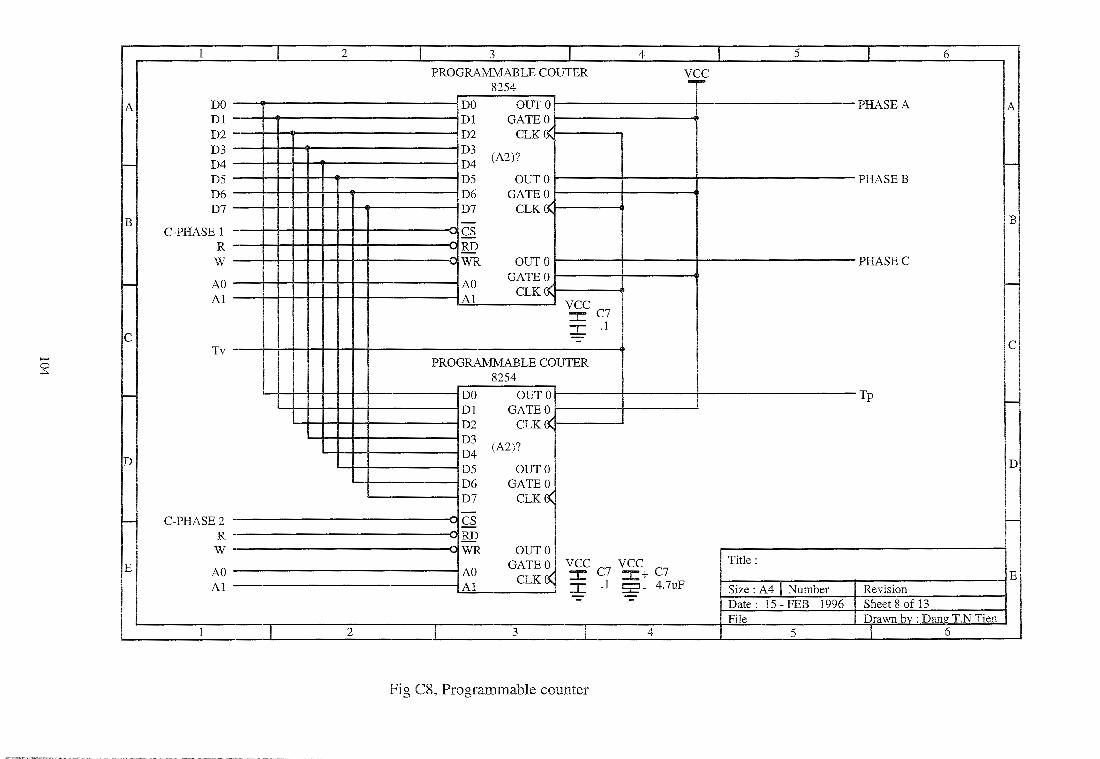
>-' 0 ~
A
-
B
-
e
-
D
-
E
1 2
DO Dl D2 D3 D4 D5 D6 D7
e-PHASE 1 -R-w-AO-Al
Tv -
e-PHASE2 -R -w-AO-Al -
1 _I 2 -
I 3 I 4
PROGRAMMABLE eOUTER vee 8254 --
DO OUTO Dl GATEO D2 eLK o( D3
(A2)? D4 D5 OUTO D6 GATEO D7 eLK o( -
~ es _,., RD ~-
-WR OUTO
AO GATEO
eLKri Al vee :r: e7
:c .1
PROGRAMMABLE eOUTER 8254
DO OUTO Dl GATEO D2 eLK 0:: D3 (A2)? D4 D5 OUTO D6 GATEO D7 eLKO:: -es RD WR OUTO
GATEO vee vee AO
eLK 0:: :r: e7 :I:+ e1 A1 :C .1 5::'- 4.7uF - -- -
I _____ 3 __ _j ______ 4_--
Fig C8, Programmable counter
5 I 6
PHASE A A
~ PHASEB
B
PHASEe
-
e
Tp f-
D
-
Title: E
Size : A4 I Number Revision Date : 15- FEB 1996 Sheet 8 of 13 File Drawn bY_: Dang T.N Tien
5 I 6
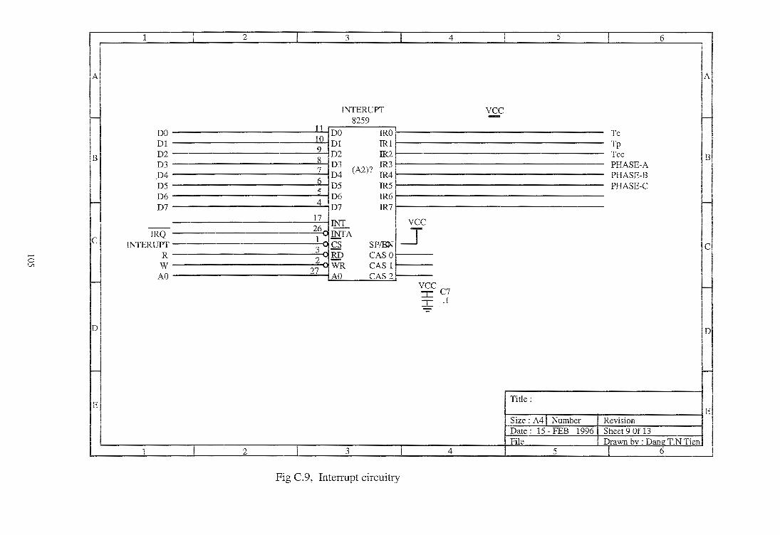
,..... 0 V1
A
-
B
-
c
r-
D
r-
E
1 I 2
DO D1 D2 D3 D4 D5 D6 D7
--· IRQ
INTERUPT R w
AO
1 - -- L__ 2
l 3
INTERUPT 8259
11 DO IRO lODl IRl 9 D2 IR2 8 D3
(A2)? IR3 7 D4 . IR4 6 D5 IRS S D6 IR6 4 D7 IR7
17 INT
26 1
INTA -3
cs SP!'EN
2 RD CASO
27 WR CAS 1 AO CAS2
L __ 3 -
Fig C.9, Interrupt circuitry
I 4 5 I 6
A
vee r-
Te Tp Tee B PHASE-A PHASE-B PHASE-C
r-
vee _T
c
vee :r: C7 I .1
r-
D
-
Title:
E Size : A4l Number Revision Date: 15- FEB 1996 Sheet 9 Of 13 File Drawn bv : Dan_g_ T.N Tien
I 4 5 I 6
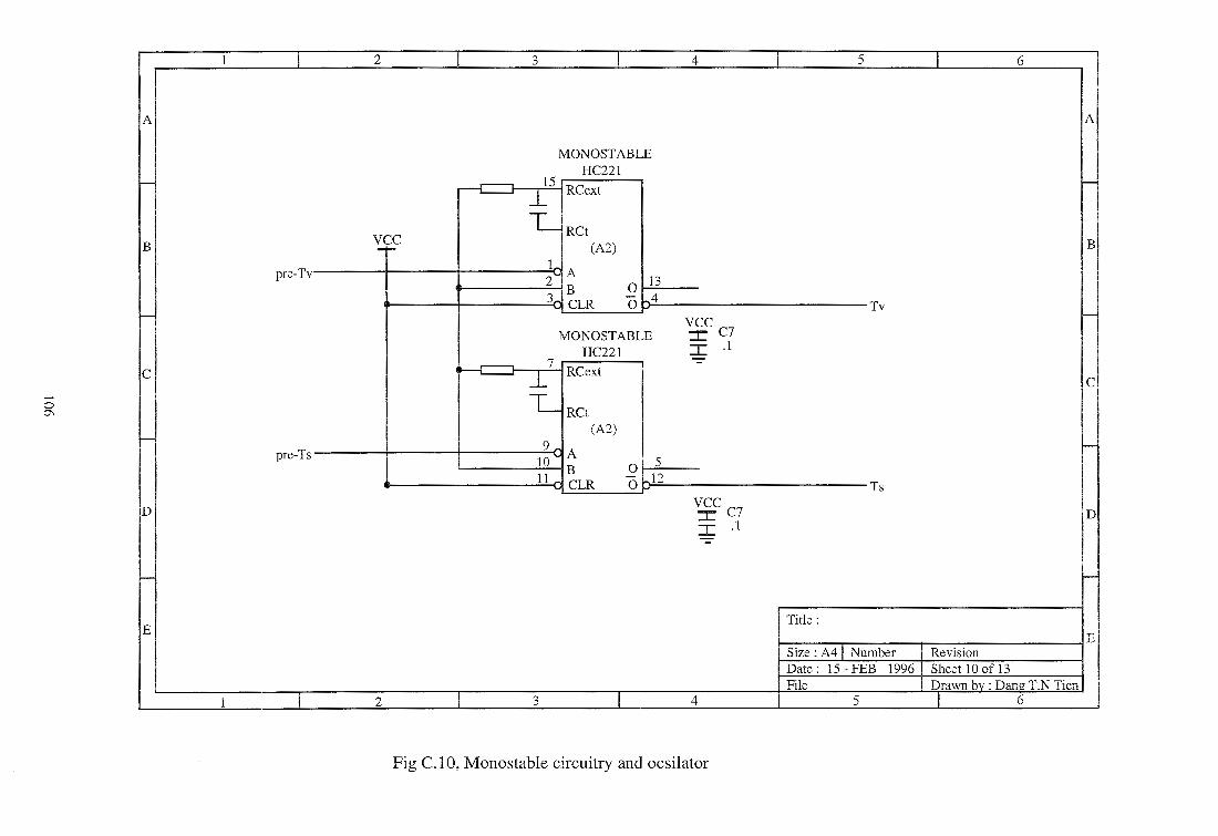
,...... 0 0\
A
-
B
-
e
-
D
-
E
--
1 I
pre-Tv
pre-Ts
1 I
2 3 I 4
MONOSTABLE He221
.-------. 15 ~ j_ Reext
L Ret vee
(A2) -~ 1
A 2~ 13 B 0
3 eLR 0 4
vee MONOSTABLE ::C e7
He221 I .1
~ j_7 Reext
L Ret (A2)
9 10
A 5
B 0 11 eLR 0 12
vee e ::r:7 I .1
2 3 I 4
Fig C.l 0, Monostable circuitry and ocsilator
5 I 6
A!
:--
B
Tv f-
e
f-
Ts
D
-
Title:
E Size : A41 Number Revision Date: 15- FEB 1996 Sheet 10 of 13 File Drawn bv : Dang T.N Tien
5 I 6
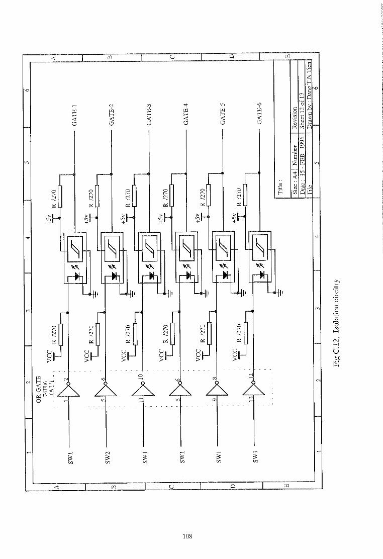
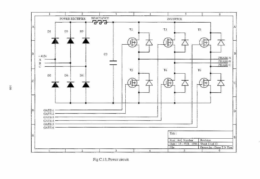
2 3 4 5 6
POWER RECTIFIER REACTANCE INVERTER
AI Dll J J rarara 1 I I l lA
T1 T3 T5
I~
co 1 Bl
f~ B
PHASE-A PHASE-B
T PHASE-C
T2 T4 T6
D2 I D4 D6
cl ~~ ""'"r" ""'"r" I I I I 1+1 1\. I I 11+1 /\. I I 11+1 1\. !C
,..... I I 0 \0
Dl GATE-1- D GATE-2-GATE-3-GATE-4-GATE-5-GATE-6-
I E
Title:
I Size: A41 Number I IE Date : 15- FEB 1996 File
1 2 3 4 5
Fig C.13, Power circuit

![cdn.instructables.com · Web view[7] “Android Mobile Phone Controlled Bluetooth Robot. Using 8051 Microcontroller” proceedings of, July 2014 ISSN (Online): 2347‐3878, Volume](https://img.pdfslide.us/doc/110x75/5e892ec38d6bb048d5676dfb/cdn-web-view-7-aoeandroid-mobile-phone-controlled-bluetooth-robot-using-8051.jpg)