Embed Size (px)
Citation preview
© Fraunhofer IST
Deposition of TCO films by Atomic Layer Deposition (ALD)
Gurram Sanjeev Kumar
Fraunhofer Institute for Surface Engineering and Thin Films (IST), Germany
TCM-2010, 3rd International Symposium on Transparent Conductive Materials
ORAMA Summer School ,15-17 Oct, 2010
© Fraunhofer IST
Outline
ALD Fundamentals
ALD of TCOs
ALD in ORAMA Project
Summary

© Fraunhofer IST
Atomic Layer Deposition Fundamentals
Introduction
Atomic Layer Deposition follows
- Sequential steps from [1] to [4] - Self limiting property- Reaction completion/cycle- No gas phase reactions
Beneq Oy
Matti Putkonen and lauri Niinisto, 2005
Condensation Dec
ompo
sitio
n
Desorption
Low
rea
ctiv
ity
Low reactive sitesEa – activation energyEd - desorption energy
T. Suntola, M.S. Report 4, 1989

© Fraunhofer IST
Atomic Layer Deposition Fundamentals
Comparision with other techniques
Technology Backgrounder: Atomic Technology Backgrounder: Atomic Layer Deposition," IC Knowledge LLC, Layer Deposition," IC Knowledge LLC, 24 April 06. 24 April 06.
VTT Finland
Properties
PVD CVD ALD
Uniformity ~80 Å range
~10 Å range
Å range
Conformity < 50% < 70% 100%
Cleanliness Particles Particles No particles
Vacuum High High /Med. Medium
Temp. range
Low Low Wide
Technology ~100 nm ~90 – 65nm
No limit
© Fraunhofer IST
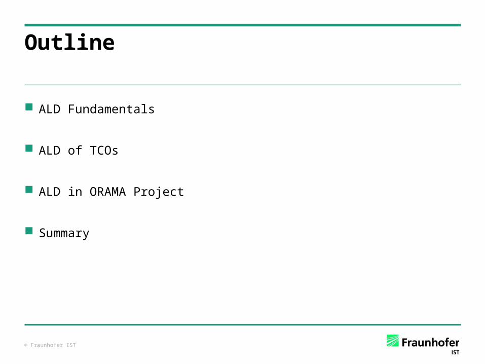
Atomic Layer Deposition Fundamentals
History
Picosun Oy Beneq Oy

© Fraunhofer IST
Atomic Layer Deposition Fundamentals
Thermal ALD
Beneq Oy
-Thermal energy is the main source
- ALD without radicals or plasma
-Negative H (heat of reactions, sponteneous at any temperature)(eg. ZnO, Al2O3, CdS ..)

© Fraunhofer IST
Atomic Layer Deposition Fundamentals
Plasma Enhanced ALD (PEALD)
PEALD is a useful extenstion of thermal ALD adding additional capabilties:
- Low temperatures and higher deposition rates (eg. SiO2 )- Enhanced film quality and tunability- It has good film adhesion than thermal ALD (Creation of more active sites)- Enhances reaction chemistry for specific films- Cycle time can be lowered ( easy switch on and off of plasma)- It helps in the deposition of single elements ( eg. Noble metals like Pt, Cu..)
Beneq Oy
Steven M George, Chem. Rev. 2010
© Fraunhofer IST
Atomic Layer Deposition Fundamentals
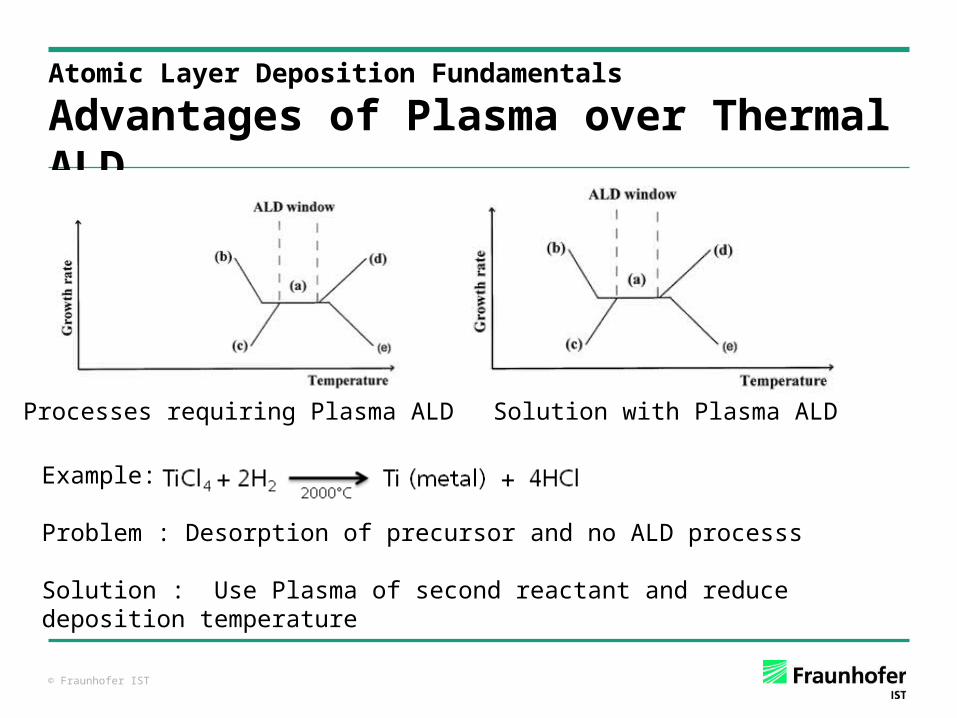
Advantages of Plasma over Thermal ALD
Processes requiring Plasma ALD
Example:
Problem : Desorption of precursor and no ALD processs
Solution : Use Plasma of second reactant and reduce deposition temperature
Solution with Plasma ALD
© Fraunhofer IST
Atomic Layer Deposition Fundamentals
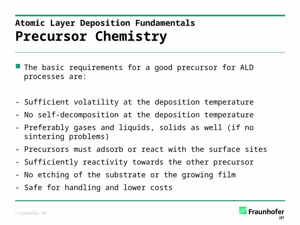
Precursor Chemistry
The basic requirements for a good precursor for ALD processes are:
- Sufficient volatility at the deposition temperature
- No self-decomposition at the deposition temperature
- Preferably gases and liquids, solids as well (if no sintering problems)
- Precursors must adsorb or react with the surface sites
- Sufficiently reactivity towards the other precursor
- No etching of the substrate or the growing film
- Safe for handling and lower costs

© Fraunhofer IST
Atomic Layer Deposition Fundamentals
Precursor ChemistryInorganic
Metal Halides
Metallo organic
ß-diketone complexes and Alkoxides
Organo metallic
Adv: Thermal stability Reactivity
Disadv: By products Vapour pressure
Adv: Vapour pressure
Disadv: Thermal stability Reactivity Molecule size
Adv: Thermal stability Reactivity By products Vapour pressure
Disadv: Cost and availability
H2O or O3 are commonly used as one of the reactant for Oxide materials
© Fraunhofer IST
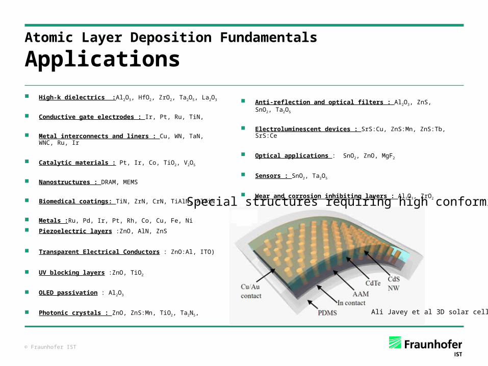
High-k dielectrics :Al2O3, HfO2, ZrO2, Ta2O5, La2O3
Conductive gate electrodes : Ir, Pt, Ru, TiN,
Metal interconnects and liners : Cu, WN, TaN, WNC, Ru, Ir
Catalytic materials : Pt, Ir, Co, TiO2, V2O5
Nanostructures : DRAM, MEMS
Biomedical coatings: TiN, ZrN, CrN, TiAlN, AlTiN
Metals :Ru, Pd, Ir, Pt, Rh, Co, Cu, Fe, Ni
Piezoelectric layers :ZnO, AlN, ZnS
Transparent Electrical Conductors : ZnO:Al, ITO)
UV blocking layers :ZnO, TiO2
OLED passivation : Al2O3
Photonic crystals : ZnO, ZnS:Mn, TiO2, Ta2N5,
Anti-reflection and optical filters : Al2O3, ZnS, SnO2, Ta2O5
Electroluminescent devices : SrS:Cu, ZnS:Mn, ZnS:Tb, SrS:Ce
Optical applications : SnO2, ZnO, MgF2
Sensors : SnO2, Ta2O5
Wear and corrosion inhibiting layers : Al2O3, ZrO2
Atomic Layer Deposition Fundamentals
Applications
Special structures requiring high conformity
Ali Javey et al 3D solar cells

© Fraunhofer IST
ALD of Transparent Conductive Oxides
TCOs Deposition and Types
There are different TCOs :
N-type TCOs P-type TCOs
ZnO based for eg. ZnO, ZnO:Al CuO based for eg. CuO, CuAlOx
ZnSn2O4 , ITO, SnO2 (delafossite structures), ZnO based amorphous Spinel structures, ZnO:N
The main important parameters for deposition of the TCO layers by ALD
- Precursors
- Growth temperature
- Type of ALD used (Thermal or Plasma)

© Fraunhofer IST
ALD of Transparent Conductive Oxides
ZnO based TCO
Zinc alkyl compounds
DEZ (Diethyl
Zinc)
DEZ (Diethyl
Zinc)
DMZ (Dimethyl
Zinc)
DMZ (Dimethyl
Zinc)+
H2O/O3
Precursor choice
The important precursors for Zinc Oxide deposition are
C2H5-Zn-C2H5 CH3-Zn-CH3
C2H5-Zn-C2H5 + H2O ZnO + 2C2H6
CH3-Zn-CH3 + H2O ZnO + 2CH4
C2H5-Zn-C2H5 + O3 ZnO + COx +H2O
CH3-Zn-CH3 + O3 ZnO + COx +H2O

© Fraunhofer IST
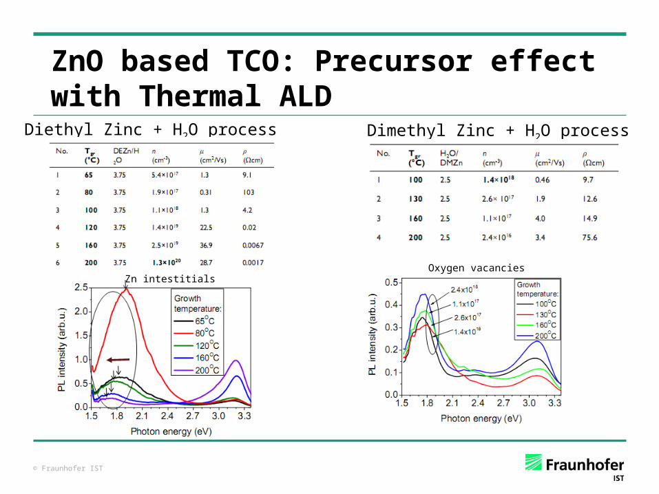
ZnO based TCO: Precursor effect with Thermal ALD
Dimethyl Zinc + H2O processDiethyl Zinc + H2O process
104 – 200 °C 100 – 150 °C
-Higher growth rate with DMZ because of Steric effect (molecular size)
-Decrease of growth rate at high temp.:- due to dehydroxylation
- Orientation in the ALD window is <100> direction and above 200°C is <200>
Grzegory Luka et al, Poland, Baltic ALD 2010 & GerALD2 in Hamburg, [1]
© Fraunhofer IST
Diethyl Zinc + H2O process Dimethyl Zinc + H2O process
ZnO based TCO: Precursor effect with Thermal ALD
Zn intestitialsOxygen vacancies

© Fraunhofer IST
ZnO based TCO: Precursor effect with Plasma Enhanced ALD
Dimethyl Zinc + O2 processDiethyl Zinc + O2 process
75 – 150 °C [*]
(104 – 200, thermal ALD)
85 – 125 °C
(100 – 150, thermal ALD)
-The growth rate of both precursors are higher than Thermal ALD
-The <002> orientation is obtained 50°C below 200°C (unlike Thermal ALD)
- Resistivities are relatively lower to the thermal ALD : Hydrogen incorporation
*Sang-Hee Ko Park et al, Elec. Solid-State Lett., 2006, Vol. 9
© Fraunhofer IST
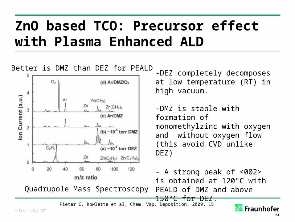
ZnO based TCO: Precursor effect with Plasma Enhanced ALD
Better is DMZ than DEZ for PEALD-DEZ completely decomposes at low temperature (RT) in high vacuum.
-DMZ is stable with formation of monomethylzinc with oxygen and without oxygen flow (this avoid CVD unlike DEZ)
- A strong peak of <002> is obtained at 120°C with PEALD of DMZ and above 150°C for DEZ.Quadrupole Mass Spectroscopy
Pieter C. Rowlette et al, Chem. Vap. Deposition, 2009, 15

© Fraunhofer IST
ALD of Transparent Conductive Oxides
ZnO based TCO: ALD of ZnO with O3
C2H5-Zn-C2H5 + H2O ZnO + 2C2H6
C2H5-Zn-C2H5 + O3 ZnO + COx +H2O
Properties:
- ZnO with Ozone occurs at high temp.
- Hydroxyl desorption at high temp.
- ZnO ( O3 process) – SAW applications
- ZnO (H2O process) – TCO applications
- Increase in resistivity - aggresive O3 - Si diffusion in to the films
O3 H2O
Seong Keun Kim et al, Thin Solid Films 478, 2005

© Fraunhofer IST
ALD of Transparent Conductive Oxides
ZnO doped TCOs :ZnO:Al
For a film thickness of 200 nm
Grzegory Luka et al, Poland, Baltic ALD 2010 & GerALD2 in Hamburg

© Fraunhofer IST
ALD of Transparent Conductive Oxides
ZnO based P-TCOs : ZnO: N
Initial reaction mechanism by DFT(Lin Dong et al, Thin Solid Films 517, 2009)Chongmu Lee et al, Materials Letters 61, 2007
Doping of Zinc Oxide with Nitrogen
© Fraunhofer IST
ALD of Transparent Conductive Oxides
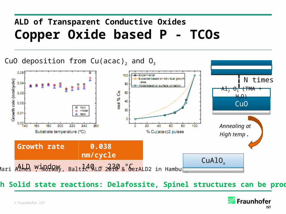
Copper Oxide based P - TCOs
Growth rate 0.038 nm/cycle
ALD window 140 – 230 °C
CuO deposition from Cu(acac)2 and O3
Mari Alnes , Norway, Baltic ALD 2010 & GerALD2 in Hamburg
With Solid state reactions: Delafossite, Spinel structures can be produced
CuOCuO
Al2 O3 (TMA + H2O)
CuAlOxCuAlOx
Annealing at
High temp.
N times
© Fraunhofer IST
ALD in ORAMA Project
To develop low defect density electronics with ALD
Deposition of Amorphous n-TCOs like Zn-Sn-O and Zn-Ga-Sn-O with ALD
Deposition of N-type ZnO and ZnMgO (counterpart to crystalline based p-n junction) having mobilities with high homogeneity and uniformity, using ALD technique.
ZnMgO to be deposited by ALD as new material for Ag seed layer
Novel ALD deposition of Poly-Crystalline (P type Active Semiconductor Oxides) e.g. Delafossite structures.
Single crystalline films to be grown on crystalline substrate

© Fraunhofer IST
Summary
A brief introduction to ALD process
Precursors effect on TCOs deposition
Different effects of Thermal and Plasma ALD on TCOs
ORAMA project goals with ALD
Thank you