Embed Size (px)
Citation preview

6T SRAMBitcell Design
Architecture
SummaryIntroducti
on
• IntroductionIntroduction• SRAM OverviewSRAM Overview• Novel SRAM bitcellNovel SRAM bitcell• Test Chip ArchitectureTest Chip Architecture• SummarySummary
Lecture ContentsLecture Contents

6T SRAMBitcell Design
Architecture
SummaryIntroducti
on
Memory is classified by 4 major categoriesMemory is classified by 4 major categoriesVolatility, Access Speed, Capacity and CostVolatility, Access Speed, Capacity and Cost
Memory ClassificationMemory Classification
Volatile Non Volatile
6T SRAMBitcell Design
Architecture
SummaryIntroducti
on
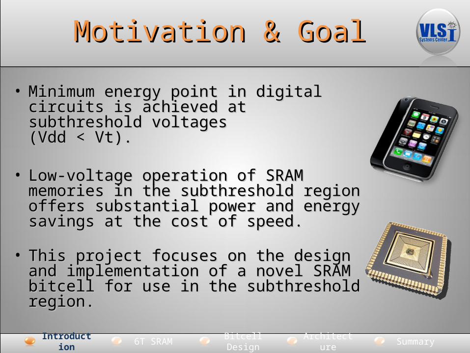
• Minimum energy point in digital circuits Minimum energy point in digital circuits is achieved at subthreshold voltages is achieved at subthreshold voltages (Vdd < Vt).(Vdd < Vt).
• Low-voltage operation of SRAM Low-voltage operation of SRAM memories in the subthreshold region memories in the subthreshold region offers substantial power and energy offers substantial power and energy savings at the cost of speed.savings at the cost of speed.
• This project focuses on the design and This project focuses on the design and implementation of a novel SRAM bitcell implementation of a novel SRAM bitcell for use in the subthreshold region.for use in the subthreshold region.
Motivation & GoalMotivation & Goal

6T SRAMBitcell Design
Architecture
SummaryIntroductio
n
SRAM OVERVIEWSRAM OVERVIEW
6T SRAMBitcell Design
Architecture
SummaryIntroductio
n
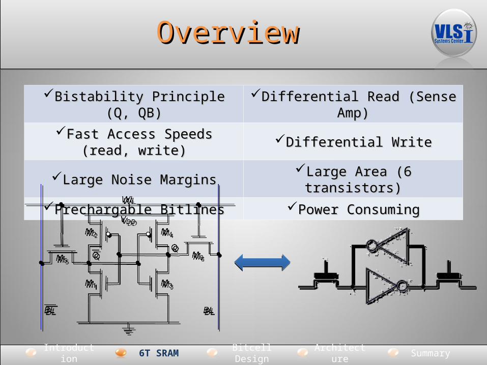
Bistability Principle (Q, QB)Bistability Principle (Q, QB) Differential Read (Sense Amp)Differential Read (Sense Amp)Fast Access Speeds (read, write)Fast Access Speeds (read, write) Differential WriteDifferential Write
Large Noise MarginsLarge Noise Margins Large Area (6 transistors)Large Area (6 transistors)Prechargable BitlinesPrechargable Bitlines Power ConsumingPower Consuming
OverviewOverview

6T SRAMBitcell Design
Architecture
SummaryIntroductio
n
• Positive feedback creates two stable points “1” and Positive feedback creates two stable points “1” and “0”.“0”.
• Regenerative property ensures a noisy cell Regenerative property ensures a noisy cell converges back to nominal values.converges back to nominal values.
Bistability – Butterfly CurveBistability – Butterfly Curve

6T SRAMBitcell Design
Architecture
SummaryIntroductio
n
1.1. Bitlines (BL, BL’) are precharged to VDDBitlines (BL, BL’) are precharged to VDD
2.2. Wordline signal (WL) is assertedWordline signal (WL) is asserted
3.3. One of the bitlines is pulled down toward GND.One of the bitlines is pulled down toward GND.
4.4. Differential signal (BL-BL’) is amplified to Differential signal (BL-BL’) is amplified to accelerate the process.accelerate the process.
SRAM – Read AccessSRAM – Read Access
WL
BL
VDD
M5
M6
M4
M1VDDVDD VDD
BL
Q = 1Q = 0
Cbit CbitMM11 > M > M55 Constr
aint!
Constraint!

6T SRAMBitcell Design
Architecture
SummaryIntroductio
n
1.1. Bitlines are precharged to complementary Bitlines are precharged to complementary values.values.
2.2. Worldline signal (WL) is asserted.Worldline signal (WL) is asserted.
3.3. Q is pulled down to GND while Q’ is driven to Q is pulled down to GND while Q’ is driven to VDD.VDD.
SRAM – Write AccessSRAM – Write Access
BL = 1 BL = 0
Q = 0
Q = 1
M1
M4
M5
M6
VDD
VDD
WL
MM66 > M > M44 Constr
aint!
Constraint!

6T SRAMBitcell Design
Architecture
SummaryIntroductio
n
• In general, ratioed digital circuits are more In general, ratioed digital circuits are more likely to fail in subthreshold voltages.likely to fail in subthreshold voltages.
• 6T Bitcells cannot operate below 6T Bitcells cannot operate below 600mV – 700mV.600mV – 700mV.
• Read SNM problem - degraded read noise Read SNM problem - degraded read noise margins decrease bitcell stability.margins decrease bitcell stability.
• Write fails under 600mV due to the Write fails under 600mV due to the increase of the pMOS drive in sub-increase of the pMOS drive in sub-threshold.threshold.
SRAM – Subthreshold ChallengesSRAM – Subthreshold Challenges

6T SRAMBitcell Design
Architecture
SummaryIntroductio
n
NOVEL 9T SRAM BITCELLNOVEL 9T SRAM BITCELL
6T SRAMBitcell Design
Architecture
SummaryIntroductio
n
The Research WorkThe Research Work
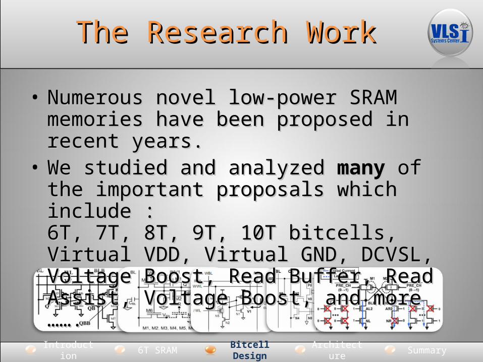
• Numerous novel low-power SRAM Numerous novel low-power SRAM memories have been proposed in memories have been proposed in recent years.recent years.
• We studied and analyzed We studied and analyzed many many of the of the important proposals which include : important proposals which include : 6T, 7T, 8T, 9T, 10T bitcells, Virtual VDD, Virtual 6T, 7T, 8T, 9T, 10T bitcells, Virtual VDD, Virtual GND, DCVSL, Voltage Boost, Read Buffer, Read GND, DCVSL, Voltage Boost, Read Buffer, Read Assist, Voltage Boost, and more …….Assist, Voltage Boost, and more …….

6T SRAMBitcell Design
Architecture
SummaryIntroductio
n
Brain StormingBrain Storming

6T SRAMBitcell Design
Architecture
SummaryIntroductio
n
• Two innovative SRAM 9T bitcells, named PSRAM Two innovative SRAM 9T bitcells, named PSRAM and SFSRAM , aimed at eliminating static power and SFSRAM , aimed at eliminating static power consumption and operated in the subthreshold consumption and operated in the subthreshold region were fully designed and analyzed.region were fully designed and analyzed.
• Three types of 8-kb 40 nm SRAM test chips, Three types of 8-kb 40 nm SRAM test chips, nicknamed nicknamed RAMBORAMBO, were designed for operation at , were designed for operation at 600mV and below.600mV and below.
Major AchievementsMajor Achievements
• We are the first academic research team inWe are the first academic research team inIsrael to fully design and fabricate a Israel to fully design and fabricate a state-of-the-art 40nm CMOS silicon chip.state-of-the-art 40nm CMOS silicon chip.

6T SRAMBitcell Design
Architecture
SummaryIntroductio
n
Chip Design WorkflowChip Design Workflow

6T SRAMBitcell Design
Architecture
SummaryIntroductio
n
Standard 8T – Schematic and LayoutStandard 8T – Schematic and Layout
NQ_NQ
PQ_PQ TQ_
TQ
WB
L
WB
L_
WW
L
WW
L_
NRB
NR
WL
RW
L
RB
L
Q_Q
Schematic of a standard 8T SRAM bitcell
QB
VVDD
PQB
PQ
NWELL
Q VDD
NFB
QB
WBLB
NQB
NQQ
QB
QB
Q
Q
QB
GNDVVDD VVDD
NFBTQ TQB
NRB QB
WWL QB
Q
WBL
RB
NRWLRBL
GND
RB
WBLB GND
QB
Q
Q
WBLRBL
WWLVDD
VDD
RWLRWL
Stick Diagram of a standard 8T SRAM bitcell

6T SRAMBitcell Design
Architecture
SummaryIntroductio
n
Pseudo static behavior - A novel bitcell Pseudo static behavior - A novel bitcell mechanism disposes of both data node mechanism disposes of both data node charges while holding a logical “1”.charges while holding a logical “1”.
Leakage current is practically Leakage current is practically eliminated during this low-power eliminated during this low-power standby mode.standby mode.
Up to Up to 3.75X3.75X less static power less static power consumption than a standard 8T consumption than a standard 8T cell at 0.9V.cell at 0.9V.
Pseudo SRAM (PSRAM)Pseudo SRAM (PSRAM)

6T SRAMBitcell Design
Architecture
SummaryIntroductio
n
WBL is driven to “1” and WBLB to “0”WBL is driven to “1” and WBLB to “0”
PSRAM – Write “1” Operation PSRAM – Write “1” Operation
Write wordline (enable) is assertedWrite wordline (enable) is asserted
Q is driven to “1” and QB to “0”Q is driven to “1” and QB to “0”
Q is discharged to during standbyQ is discharged to during standby
CLK synchronizes write accessCLK synchronizes write access

6T SRAMBitcell Design
Architecture
SummaryIntroductio
n
PSRAM – Power ReductionPSRAM – Power Reduction
1.35X

6T SRAMBitcell Design
Architecture
SummaryIntroductio
n
Enables subthreshold write with a Enables subthreshold write with a Virtual-VDD technique – weakening the Virtual-VDD technique – weakening the Supply VDD during write operation.Supply VDD during write operation.
A new approach for the design of the A new approach for the design of the Virtual-VDD scheme reduces periphery Virtual-VDD scheme reduces periphery and thus, reduces write power.and thus, reduces write power.
Operates at ultra-low voltages, down to Operates at ultra-low voltages, down to 200mV.200mV.
SFSRAM (Supply Feedback SRAM)SFSRAM (Supply Feedback SRAM)

6T SRAMBitcell Design
Architecture
SummaryIntroductio
n
Standard 8T – RevisitedStandard 8T – Revisited
NQ_NQ
PQ_PQ TQ_
TQ
WB
L
WB
L_
WW
L
WW
L_
NRB
NR
WL
RW
L
RB
L
Q_Q
Schematic of a standard 8T SRAM bitcell
QB
VVDD
PQB
PQ
NWELL
Q VDD
NFB
QB
WBLB
NQB
NQQ
QB
QB
Q
Q
QB
GNDVVDD VVDD
NFBTQ TQB
NRB QB
WWL QB
Q
WBL
RB
NRWLRBL
GND
RB
WBLB GND
QB
Q
Q
WBLRBL
WWLVDD
VDD
RWLRWL
Stick Diagram of a standard 8T SRAM bitcell

6T SRAMBitcell Design
Architecture
SummaryIntroductio
n
SFSRAM – Power ReductionSFSRAM – Power Reduction

6T SRAMBitcell Design
Architecture
SummaryIntroductio
n
40NM TEST CHIP 40NM TEST CHIP

6T SRAMBitcell Design
Architecture
SummaryIntroductio
n
• 8-kb Array8-kb Array• Read-Bitline divisionRead-Bitline division• Level ShiftersLevel Shifters• Row DecoderRow Decoder• Sense-AmpsSense-Amps• Precharge UnitsPrecharge Units• Write DriversWrite Drivers• BISTBIST
Chip ArchitectureChip Architecture
WW
L[63
:0]
RWL[
63:0
]
RBL[31:0]
Block 3
WW
L[63
:0]
RWL[
63:0
]
RBL[31:0]
Block 2
Row
Dec
oder
(8 :2
56)
Leve
l Shi
ftin
g W
ordl
ine
Driv
ers x2
56
32 x Precharge + Write Driver Units
BIST
256
256
WW
L [2
55:0
]RW
L [2
55:0
]
256
WL_
out [
255:
0]
WL
[255
:0]7
ADD_
in[7
:0]
ADD2
SRAM
[7:0
]
CLK
32
WBL[31:0]DVDD
DVSS
32
WBLB[31:0] PC
PCWBL[31:0] WBLB[31:0]
CLK
VDD
GND
CLK
DVDD
DVSS
CLK
DVDD
GND
SVDD
SVDD
CLKDVDDDVSS
CLKDVDD
GNDSVDDSVDD
32
DIN2SRAM[31:0]
DIN[31:0]
32
DIN[31:0]
DATA[31:0]
32
RBL[31:0]
32 x Sensing Unit + Level ShifterDOUT[31:0]
SRAM2DOUT[31:0]
32
32
DOUT[31:0]
DOUT[31:0]PASS_FAIL
CLKDVDDDVSS
CLKDVDD
GNDSVDDSVDD
CLK
DVDD
DVSS
CLK
VDD
GND BIST_CNTRL
8
ADD[
7:0]
ADD[7:0]
WR WR
RD RD
CS CS CS
CS2S
RAM
RD
RD2SRAM
WR
WR2SRAM
WW
L[63
:0]
RWL[
63:0
]
RBL[31:0]
Block 1
SRAM Array64x32
WW
L[63
:0]
RWL[
63:0
]
RBL[31:0]
Block 0
DVSSGND
SVDDSVDD

6T SRAMBitcell Design
Architecture
SummaryIntroductio
n
40nm Test Chip - Periphery40nm Test Chip - Periphery
GND
DVDD
GN
D
SV
DD
GN
D
SV
DD
GN
D
SV
DD
GN
D
SV
DD
RBL_0RBL_1
RBL_4 RBL_3
DATA OUT
SASA
SA SA
Schematic of Sensing Unit + Up Shifter
GNDGND
GND
ENABLEENABLE
DATA IN
SVDD SVDD SVDD
WBL_RWBL_L
Schematic of Write Driver
RD
CLK
Selected WL
Selected RWL
WR
CLK Selected WWL
Selected WL
DV
DD
SV
DD
DV
DD
SV
DD
Schematic of WL Driver + Down Shifter

6T SRAMBitcell Design
Architecture
SummaryIntroductio
n
Test Chip Top Level LayoutTest Chip Top Level Layout
1.40 mm
1.40
mm
1.40 um
2.90 um

6T SRAMBitcell Design
Architecture
SummaryIntroductio
n
Chip Timing DiagramsChip Timing Diagrams
CLK
ADDR
WR_DATA
WR
RD
Selected WL
Selected WWL
Selected RWL
Selected WBL
Selected WBLB
Selected RBL
RD_DATA
SRAM access is synchronized by a clock. Bitline Precharge, write driving and digital logic execute during the high phase
and read/write take place during the low phase.

6T SRAMBitcell Design
Architecture
SummaryIntroductio
n
SUMMARYSUMMARY
6T SRAMBitcell Design
Architecture
SummaryIntroductio
n
A fully functional 8-kb array was layed A fully functional 8-kb array was layed out and designed for the 40nm lp TSMC out and designed for the 40nm lp TSMC
process.process.
SFSRAM Memory successfully operates at SFSRAM Memory successfully operates at subthreshold voltages - no additional subthreshold voltages - no additional
periphery required.periphery required.
Additional power savings can be achieved Additional power savings can be achieved in the PSRAM with a majority bit in the PSRAM with a majority bit
algorithm.algorithm.
SummarySummary

6T SRAMBitcell Design
Architecture
SummaryIntroductio
n
PSRAM consumes up to PSRAM consumes up to 3.75X less 3.75X less static power than a standard 8T static power than a standard 8T
cell.cell.
Summary – ContinuedSummary – Continued
We Are The first academic research team in We Are The first academic research team in Israel to fully design and fabricate a Israel to fully design and fabricate a
state-of-the-art 40nm chip.state-of-the-art 40nm chip.

6T SRAMBitcell Design
Architecture
SummaryIntroductio
n
Questions??Questions??
Digital Digital ChipChip
Chocolate Chocolate ChipChip