Embed Size (px)
Citation preview

YMF825 SD-1
universal Sound Designer 1
Overview
YMF825 is a sound generator/controller/amplifier device with high quality melodies and keypad/alert tones, designed for sophisticated audio user interface on home appliances and office equipment products.
Yamaha's FM synthesizer produce high fidelity clean vivid sound, in no way comparable to the traditional beeps and chimes used in such products, yet all the control required is just a few tens of bytes of setup parameters.
As many as 16 FM voices are supported, and any host controller can manage those voices using the on-chip melody sequencer that plays tunes autonomously without host controller interventions.
Simple commands allow real time controls of sound during playback, such as changing the volume levels or the repetition intervals of tones.
Moreover, the complete system can be built with the minimum number of external components as the integrated amplifier can directly drive an 8 ohm loudspeaker attached, up to 900 mW.
YMF825 CATALOG
CATALOG No. LSI-4MF825A40
2011.9
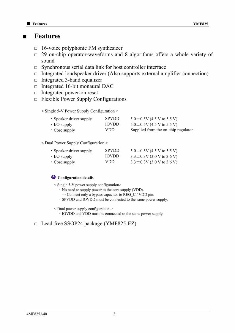
Features YMF825
Features
16-voice polyphonic FM synthesizer 29 on-chip operator-waveforms and 8 algorithms offers a whole variety of
sound Synchronous serial data link for host controller interface Integrated loudspeaker driver (Also supports external amplifier connection) Integrated 3-band equalizer Integrated 16-bit monaural DAC Integrated power-on reset Flexible Power Supply Configurations
< Single 5-V Power Supply Configuration >
・Speaker driver supply SPVDD 5.0±0.5V (4.5 V to 5.5 V) ・I/O supply IOVDD 5.0±0.5V (4.5 V to 5.5 V) ・Core supply VDD Supplied from the on-chip regulator
< Dual Power Supply Configuration >
・Speaker driver supply SPVDD 5.0±0.5V (4.5 V to 5.5 V) ・I/O supply IOVDD 3.3±0.3V (3.0 V to 3.6 V) ・Core supply VDD 3.3±0.3V (3.0 V to 3.6 V)
Configuration details
< Single 5-V power supply configuration> ・No need to supply power to the core supply (VDD). → Connect only a bypass capacitor to REG_C / VDD pin.
・SPVDD and IOVDD must be connected to the same power supply. < Dual power supply configuration >
・IOVDD and VDD must be connected to the same power supply.
Lead-free SSOP24 package (YMF825-EZ)
4MF825A40 2

Pin Assignments YMF825
4MF825A40 3
Pin Assignments
TESTOUT 1 24 XO
IRQ_N 2 23 XI
SO 3 22 TESTINB
SI 4 21 TESTINA
SCK 5 20 TESTMODE1
SS_N 6 19 TESTMODE0
RST_N 7 18 VSS
REG_C / VDD 8 17 A_TEST
IOVDD 9 16 SPOUT2 / LINEOUT2
VREF 10 15 No Connection
SPVDD 11 14 SPOUT1 / LINEOUT1
SPVSS 12 13 No Connection
24-pin SSOP TOP View

Pin Functions YMF825
4MF825A40 4
Pin Functions
No. Name I/O PowerSupply
Function
1 TESTOUT O IOVDDTest output → This pin should be left open (No Connection).
2 IRQ_N O IOVDD Interrupt output 3 SO Oe IOVDD Serial data output (CPU interface) 4 SI I IOVDD Serial data input (CPU interface) 5 SCK I IOVDD Serial clock (CPU interface) 6 SS_N I IOVDD Chip select (CPU interface)
7 RST_N Is IOVDDReset → Pull up to IOVDD when not used.
8 REG_C / VDD AO / P IOVDD
/ -
On-chip regulator capacitor connection / Core power supply → < Single 5V power supply configuration >
Connect capacitors only. < Dual power supply configuration > Supply 3.3 V (typ.) to VDD from the same power supply as
IOVDD. 9 IOVDD P - I/O power supply and on-chip regulator input 10 VREF AO VDD Analog block reference voltage 11 SPVDD P - Speaker amplifier power supply 12 SPVSS G - Speaker amplifier GND
13 (No Connection) - - This pin must be left open. (No Connection) (This pin must be electrically isolated not only from the power supply and ground pins, and adjacent pins, but also from any other pins.)
14 SPOUT1/LINEOUT1 AO SPVDD Speaker output 1 / Line output 1
15 (No Connection) - - This pin must be left open. (No Connection) (This pin must be electrically isolated not only from the power supply and ground, pins and adjacent pins, but also from any other pins.)
16 SPOUT2/LINEOUT2 AO SPVDD Speaker output 2 / Line output 2
17 A_TEST AIO IOVDDAnalog test pin → This pin should be left open (No Connection).
18 VSS G - GND
19 TESTMODE0 I IOVDDTest mode configuration → Connect to the VSS.
20 TESTMODE1 I IOVDDTest mode configuration → Connect to the VSS.
21 TESTINA I IOVDDTest input pin → Connect to the VSS.
22 TESTINB I IOVDDTest input pin → Connect to the VSS.
23 XI XI / I IOVDDCrystal connection / Clock input → The external clock cannot be used when this device is used in single
5 V power supply configuration. Use a crystal in such designs.
24 XO XO IOVDDCrystal connection → When the external clock is fed to XI pin, this pin must be left open.
AIO : Analog I/O I : Digital input XI : Crystal resonator input
AO : Analog output Is : Digital input (schmitt) XO : Crystal resonator output
P : Power O : Digital output G : GND Oe : Digital output (3-state)

Block Diagram YMF825
Block Diagram
Digital
Analog
IOVDD
VSS
IRQ_N
SCK
SI
SO
SS_NRead Access
VREF
Direct Writ e Access
VREF
Timing Gen
Regulator(5V→3.3V)
3.3V (for Digital Core &Analog Core(except SPAMP))
SPVDD
Buffer
SPVSS
(for Digital I/O)
TESTMODE1
TESTOUT
A_TEST
TESTINA
TESTINB
TESTMODE0
RST_N
Delay Writ e Access
SpeakerAmp
SPOUT1/LINEOUT1
SPOUT2/LINEOUT2
Power On Reset CircuitPower On Reset
< Timing Gen >
The timing generator block generates clocks and other timing signals required for the operations. < CPU Interface >
The CPU interface block is a 4-wire CPU serial interface. The use of the interface is based on the assumption that the following four signal lines are connected to host controller CPU: Chip Select (SS_N), Serial Clock (SCK), Data Input (SI), and Data Output (SO).
< Interface Register >
The interface register can be accessed directly from the host controller CPU via the serial interface. < Control Register >
The control register mainly controls the synthesizer block. The control register is accessed for the timed-write operations of the sequencer, and also accessed for the direct write or the read operations through the interface register.
< FIFO >
The FIFO, an abbreviation of "First In First Out", is a queue allowing data to be read in the same order they are written. The FIFO is accessed through the interface register and used in the timed-write path to the control register by the sequencer. The size of the FIFO is 512 Bytes.
4MF825A40 5

Block Diagram YMF825
< Sequencer >
The sequencer controls the de-queuing of the sequenced data queued into the FIFO. The data structure is as follows:
Timing information (Timer part) + control register address (Address part) + control register data to be written (Data part) The sequencer waits for the time of the Timer part before writing the Data part to the control register address specified (timed-write operations). This timed de-queuing of the sequenced data to control the FM synthesizer results in the playing back of the music tunes.
< FM Synthesizer >
The polyphonic FM synthesizer can generate up to 16 voices. Variety in sound authoring is provided with the wider choice of operator waveforms. The sampling frequency for the internal processing is 48 kHz.
< 3-Band Equalizer >
This is a 3-band digital equalizer. < High Pass Filter >
This filter, a first-order IIR filter, is the DC-cut high-pass filter. Its cut-off frequency is 20Hz.
< Master Volume >
This is the digital master control of overall volume level. < 16-bit DAC >
The DAC block converts the digital signals from the digital block into analog signals. The data resolution is 16 bits.
< Speaker Amp >
The speaker amplifier is the monaural speaker amplifier with four-level gain settings. < Regulator >
The linear regulator supplies 3.3V (typ.).
< Power-On Reset> This circuit resets the registers on power up. This reset works exactly the same as the hardware reset pin.
Notes on Power-On Reset
When this device is powered down and then powered up again, this power-on reset may not function unless this device is left unpowered for a sufficient time.
4MF825A40 6

Electrical Characteristics YMF825
4MF825A40 7
Electrical Characteristics
Absolute Maximum Ratings
Parameter Symbol Min. Max. Unit
SPVDD supply voltage SPVDD −0.3 7.0 V IOVDD supply voltage IOVDD −0.3 7.0 V VDD supply voltage VDD −0.3 4.6 V Digital input voltage (See Note 1.) VIND −0.3 IOVDD+0.3 V Analog input voltage VINA −0.3 IOVDD+0.3 V Power dissipation (See Note 2.) Pd 1638 mW Junction Temperature Tj 150 °C Storage Temperature TSTG −50 150 °C
Conditions VSS=SPVSS=0 V
Note1) These limits must be observed even if the supply voltage is out of the recommended operating
voltage range.
For example, when the power supply pin is at 0 V, any voltage over 0.3V is beyond the limit.
Note 2) Conditions:
• Top= 25 °C, PCB (50 mm × 50 mm × 1.6 mm), FR-2 board, trace density 50 %
• Derate the value with 13.1 mW/°C for the temperature above 25 °C.
Electrical Characteristics YMF825
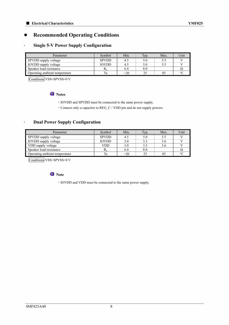
Recommended Operating Conditions
· Single 5-V Power Supply Configuration
Parameter Symbol Min. Typ. Max. Unit
SPVDD supply voltage SPVDD 4.5 5.0 5.5 V IOVDD supply voltage IOVDD 4.5 5.0 5.5 V Speaker load resistance RL 6.4 8.0 Ω Operating ambient temperature Ta −20 25 85 °C
Conditions VSS=SPVSS=0 V
Notes
・IOVDD and SPVDD must be connected to the same power supply.
・Connect only a capacitor to REG_C / VDD pin and do not supply powers.
· Dual Power Supply Configuration
Parameter Symbol Min. Typ. Max. Unit
SPVDD supply voltage SPVDD 4.5 5.0 5.5 V IOVDD supply voltage IOVDD 3.0 3.3 3.6 V VDD supply voltage VDD 3.0 3.3 3.6 V Speaker load resistance RL 6.4 8.0 Ω Operating ambient temperature Ta −20 25 85 °C
Conditions VSS=SPVSS=0 V
Note
・IOVDD and VDD must be connected to the same power supply.
4MF825A40 8

Electrical Characteristics YMF825
4MF825A40 9
Power Consumption
All the drawn current values in the tables are typical representative values to help your design decisions.
· Single 5-V Power Supply Configuration
Parameter Conditions IOVDD SPVDD Unit
No signal output 5 mADrawn current, normal operation (AP*=all “0”, CLKE=“1”) RL=8Ω load, f=1kHz, 400mW
17 200 mA
Drawn current, power-down (AP0=“0”, AP[1/2/3]= “1”, CLKE=“0”)
VIL=VSS, VIH=IOVDD 5 0 mA
Conditions SPVDD = IOVDD = 5.0 V, room temperature.
· Dual Power Supply Configuration
i) Use of Crystal Resonator
Parameter Conditions IOVDD (+ VDD)
SPVDD Unit
No signal output 5 mADrawn current, normal operation (AP*=all “0”, CLKE=“1”) RL=8Ω load, f=1kHz, 400mW
15 200 mA
Drawn current, power-down (AP0=“0”, AP[1/2/3]= “1”, CLKE=“0”)
VIL=VSS, VIH=IOVDD 3 0 mA
Conditions SPVDD = 5.0 V, IOVDD = VDD = 3.3 V, room temperature. ii) Use of External Clock
Parameter Conditions IOVDD (+ VDD)
SPVDD Unit
No signal output 5 mADrawn current, normal operation (AP*=all “0”, CLKE=“1”) RL=8Ω load, f=1kHz, 400mW
14 200 mA
Drawn current, power-down (AP0=“0”, AP[1/2/3]= “1”, CLKE=“0”)
VIL=VSS, VIH=IOVDD 2 0 mA
Conditions SPVDD = 5.0 V, IOVDD = VDD = 3.3 V, room temperature. XI pin: 12.288 MHz clock, XO pin: No connection

Electrical Characteristics YMF825
DC Characteristics
Parameter Symbol Condition Min. Typ. Max. Unit
Input Voltage “H” level (1) VIH (See Note 1.) 0.80 IOVDD V Input Voltage “L” level (1) VIL (See Note 1.) 0.20 IOVDD V Input Voltage “H” level (2) VIH (See Note 2.) 0.70 IOVDD V Input Voltage “L” level (2) VIL (See Note 2.) 0.30 IOVDD V Output Voltage “H” level (1) VOH IOH =
(See Note 3.) 0.80 IOVDD V
Output Voltage “L” level (1) VOL IOL = (See Note 3.)
0.20 IOVDD V
Schmitt hysteresis width Vsh (See Note 4.) 0.20 IOVDD mV Input leakage current IL −10 10 A Input capacitance CI 10 pF
Conditions Capacitor load=30pF. For operations under the recommended operating conditions
Note 1: RST_N pin only
Note 2: SI, SCK, SS_N, and XI (only when an external clock is used) pins only
Note 3: IRQ_N: 2mA
SO: 4mA
Note 4: RST_N only
Note
Consider the use of signal damping resistors where appropriate, in product designs.
4MF825A40 10
Electrical Characteristics YMF825
AC Characteristics
Power Supply Timing Requirements
Either requirements A or B must be met:
Requirement A
Parameter Symbol Min. Typ. Max. Unit
Supply voltage rise time (See Note 1.) TVRISE 10 ms
Power off interval (See Note 2.) TVOFF 100 ms
Conditions For operations under the recommended operating conditions
Requirement B Parameter Symbol Min. Typ. Max. Unit
Supply voltage rise time (See Note 1.) TVRISE 10 ms
Reset_N "L" pulse width TRSTW 1 ms Reset_N (undefined →" L") Setup Time TRSTS 0 μs
Conditions For operations under the recommended operating conditions
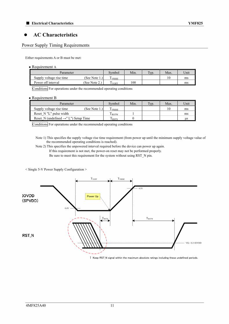
Note 1) This specifies the supply voltage rise time requirement (from power up until the minimum supply voltage value of the recommended operating conditions is reached).
Note 2) This specifies the unpowered interval required before the device can power up again. If this requirement is not met, the power-on reset may not be performed properly. Be sure to meet this requirement for the system without using RST_N pin.
< Single 5-V Power Supply Configuration >
TVOFF
0.4V
TRSTS TRSTW
VIL= 0.2×IOVDD
4.5V
TVRISE
Power Up
↑ Keep RST_N signal within the maximum absolute ratings including these undefined periods.
4MF825A40 11

Electrical Characteristics YMF825
< Dual Power Supply Configuration >
TVOFF
0.4V
TRSTS TRSTW
VIL= 0.2×IOVDD
3.0V
TVRISE
Power Up
↑ Keep RST_N signal within the maximum absolute ratings including these undefined periods.
4.5V
TVRISE
Power Up
Notes
< Single 5-V Power Supply Configuration >
・IOVDD and SPVDD must be connected to the same power supply.
< Dual Power Supply Configuration >
・IOVDD and VDD must be connected to the same power supply.
4MF825A40 12

Electrical Characteristics YMF825
Input Clock (XI) Requirements
Parameter Symbol Min. Typ. Max. Unit
XI frequency 1 / Tfreq 12.288 MHz XI Rise time, Fall time (See Note 1.) Trckc, Tfckc 20 ns XI High time (See Note 1.) Th 20 ns XI Low time (See Note 1.) Tl 20 ns Frequency tolerance - −100 +100 ppm
Conditions For operations under the recommended operating conditions
Note 1) These values specify the requirements for the external clocks on XI pin.
Tfreq
XIVIH= 0.7×IOVDD
VIL= 0.3×IOVDD
0.5×IOVDD
Trckc Tfckc
Th Tl
4MF825A40 13
Electrical Characteristics YMF825
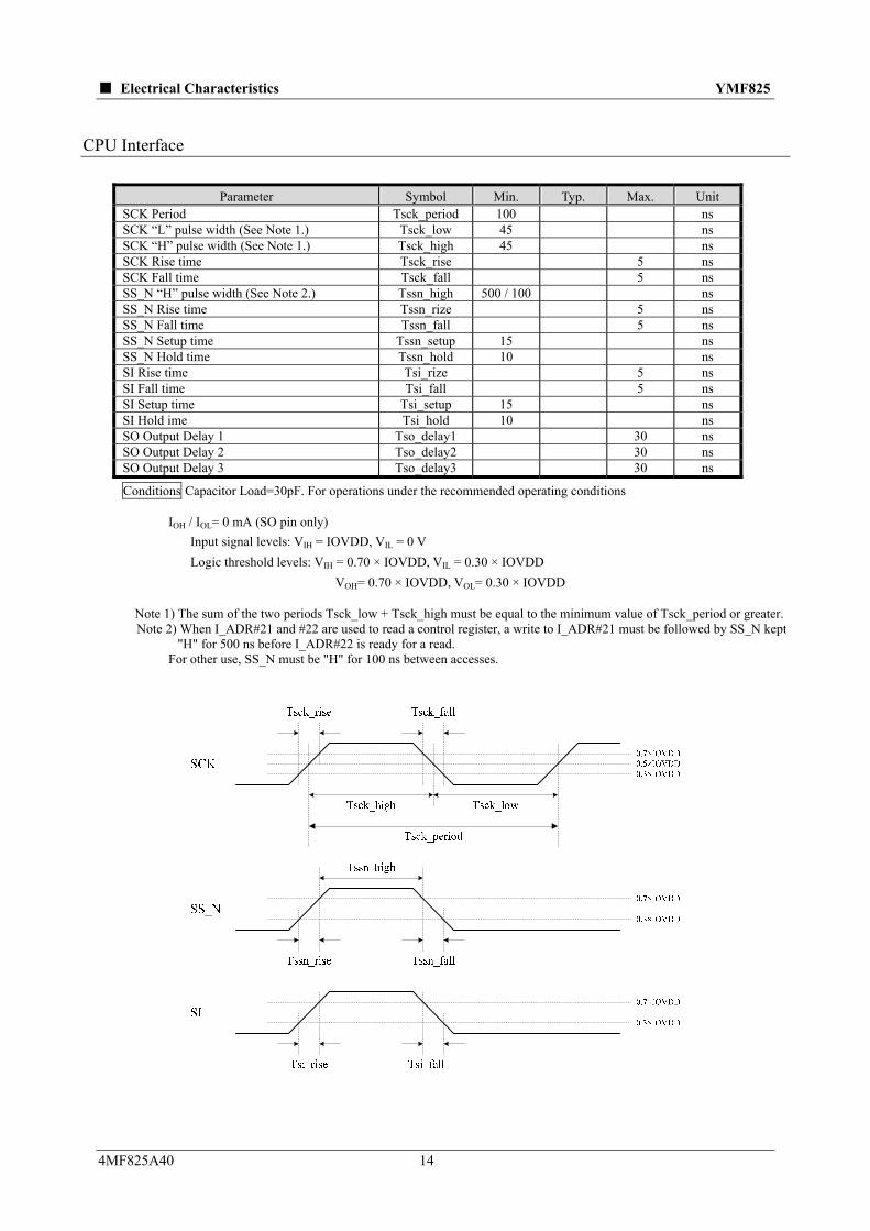
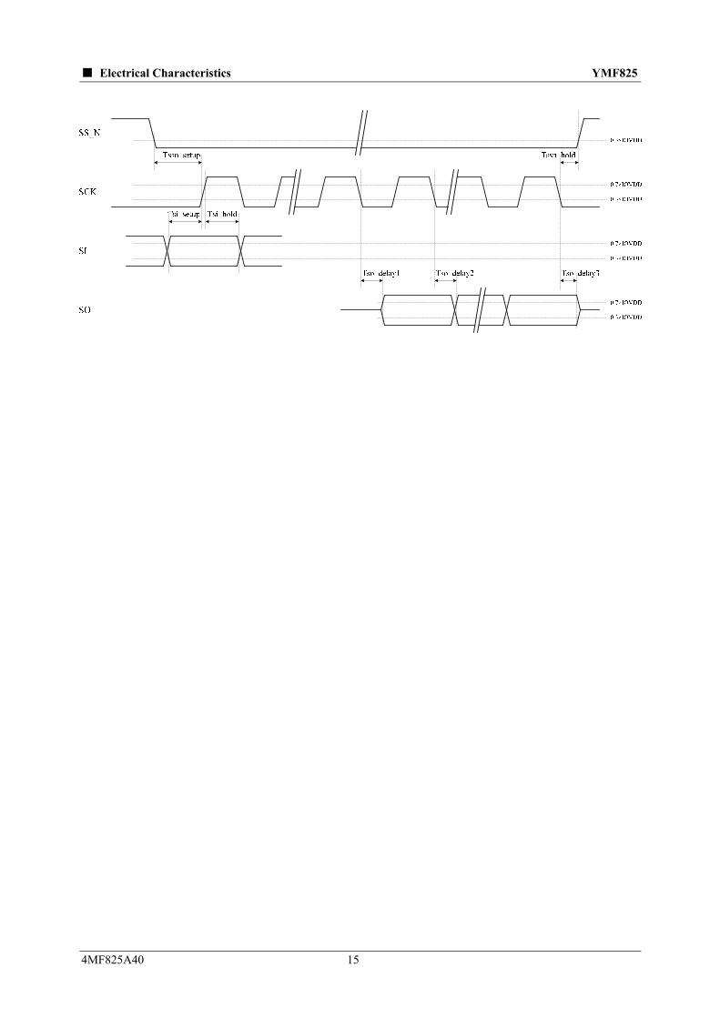
CPU Interface
Parameter Symbol Min. Typ. Max. Unit SCK Period Tsck_period 100 ns SCK “L” pulse width (See Note 1.) Tsck_low 45 ns SCK “H” pulse width (See Note 1.) Tsck_high 45 ns SCK Rise time Tsck_rise 5 ns SCK Fall time Tsck_fall 5 ns SS_N “H” pulse width (See Note 2.) Tssn_high 500 / 100 ns SS_N Rise time Tssn_rize 5 ns SS_N Fall time Tssn_fall 5 ns SS_N Setup time Tssn_setup 15 ns SS_N Hold time Tssn_hold 10 ns SI Rise time Tsi_rize 5 ns SI Fall time Tsi_fall 5 ns SI Setup time Tsi_setup 15 ns SI Hold ime Tsi_hold 10 ns SO Output Delay 1 Tso_delay1 30 ns SO Output Delay 2 Tso_delay2 30 ns SO Output Delay 3 Tso_delay3 30 ns
Conditions Capacitor Load=30pF. For operations under the recommended operating conditions IOH / IOL= 0 mA (SO pin only)
Input signal levels: VIH = IOVDD, VIL = 0 V
Logic threshold levels: VIH = 0.70 × IOVDD, VIL = 0.30 × IOVDD
VOH= 0.70 × IOVDD, VOL= 0.30 × IOVDD
Note 1) The sum of the two periods Tsck_low + Tsck_high must be equal to the minimum value of Tsck_period or greater. Note 2) When I_ADR#21 and #22 are used to read a control register, a write to I_ADR#21 must be followed by SS_N kept
"H" for 500 ns before I_ADR#22 is ready for a read. For other use, SS_N must be "H" for 100 ns between accesses.
4MF825A40 14
Electrical Characteristics YMF825
4MF825A40 15
Electrical Characteristics YMF825
4MF825A40 16
Analog Characteristics
The measurement conditions are as follows:
TOP=25 °C
IOVDD=SPVDD=5 V
GAIN[1:0]= "1"(6.5 dB), RL=8Ω, CREG_OUT=4.7μF, CVREF=1μF
Parameter Min. Typ. Max. Unit
Maximum Output Power GAIN[1:0]= "2’b11"(7.5dB) 900 mW Maximum Output Voltage Amplitude GAIN[1:0]= "2’b11"(7.5dB)
7.58 Vp-p
Output Offset Voltage 10 50 mV Quiescent Output Voltage 2.50 V Frequency Characteristics (50Hz to 20kHz, with reference to the 1kHz level)
−3.5 0.5 dB
Total Harmonic Distortion (1kHz, 400mW, 22kHz LPF)
0.3 %
Residual Noise Level (A-weighted) -85 dBV Capacitive Load on Speaker Output 1000 pF VREF Voltage 1.65 V VREF Settling Time 30 ms On-chip Regulator Output Voltage 3.3 V On-chip Regulator Settling Time 27 100 μs

Package Information YMF825
Package Information
4MF825A40 17

YMF825
4MF825A40 18
PRECAUTIONS AND INSTRUCTIONS FOR SAFETY
WARNING
Prohibited
Do not use the device under stresses beyond those listed in Absolute Maximum Ratings. Such stresses may become causes of breakdown, damages, or deterioration, causing explosion or ignition, and this may lead to fire or personal injury.
Prohibited
Do not mount the device reversely or improperly and also do not connect a supply voltage in wrong polarity. Otherwise, this may cause current and/or power-consumption to exceed the absolute maximum ratings, causing personal injury due to explosion or ignition as well as causing breakdown, damages, or deterioration. And, do not use the device again that has been improperly mounted and powered once.
Prohibited
Do not short between pins. In particular, when different power supply pins, such as between high-voltage and low-voltage pins, are shorted, smoke, fire, or explosion may take place.
Instructions
As to devices capable of generating sound from its speaker outputs, please design with safety of your products and system in mind, such as the consequences of unusual speaker output due to a malfunction or failure. A speaker dissipates heat in a voice-coil by air flow accompanying vibration of a diaphragm. When a DC signal (several Hz or less) is input due to device failure, heat dissipation characteristics degrade rapidly, thereby leading to voice-coil burnout, smoking or ignition of the speaker even if it is used within the rated input value.
CAUTION
Prohibited
Do not use Yamaha products in close proximity to burning materials, combustible substances, or inflammable materials, in order to prevent the spread of the fire caused by Yamaha products, and to prevent the smoke or fire of Yamaha products due to peripheral components.
Instructions
Generally, semiconductor products may malfunction and break down due to aging, degradation, etc. It is the responsibility of the designer to take actions such as safety design of products and the entire system and also fail-safe design according to applications, so as not to cause property damage and/or bodily injury due to malfunction and/or failure of semiconductor products.
Instructions
The built-in DSP may output the maximum amplitude waveform suddenly due to malfunction from disturbances etc. and this may cause damage to headphones, external amplifiers, and human body (the ear). Please pay attention to safety measures for device malfunction and failure both in product and system design.
Instructions
As semiconductor devices are not nonflammable, overcurrent or failure may cause smoke or fire. Therefore, products should be designed with safety in mind such as using overcurrent protection circuits to control the amount of current during operation and to shut off on failure.
Instructions
Products should be designed with fail safe in mind in case of malfunction of the built-in protection circuits. Note that the built-in protection circuits such as overcurrent protection circuit and high-temperature protection circuit do not always protect the internal circuits. In some cases, depending on usage or situations, such protection circuit may not work properly or the device itself may break down before the protection circuit kicks in.
Instructions
Use a robust power supply. The use of an unrobust power supply may lead to malfunctions of the protection circuit, causing device breakdown, personal injury due to explosion, or smoke or fire.
Instructions
Product's housing should be designed with the considerations of short-circuiting between pins of the mounted device due to foreign conductive substances (such as metal pins etc.). Moreover, the housing should be designed with spatter prevention etc. due to explosion or burning. Otherwise, the spattered substance may cause bodily injury.
Instructions
The device may be heated to a high temperature due to internal heat generation during operation. Therefore, please take care not to touch an operating device directly.
v02
YMF825
eC02