Embed Size (px)
Citation preview
MOS Model 20-- a versatile LDMOS model --
A.C.T. Aarts * and D.B.M. Klaassen **
* Eindhoven University of Technology
** Philips Research Laboratories
EindhovenThe Netherlands
HTU/e
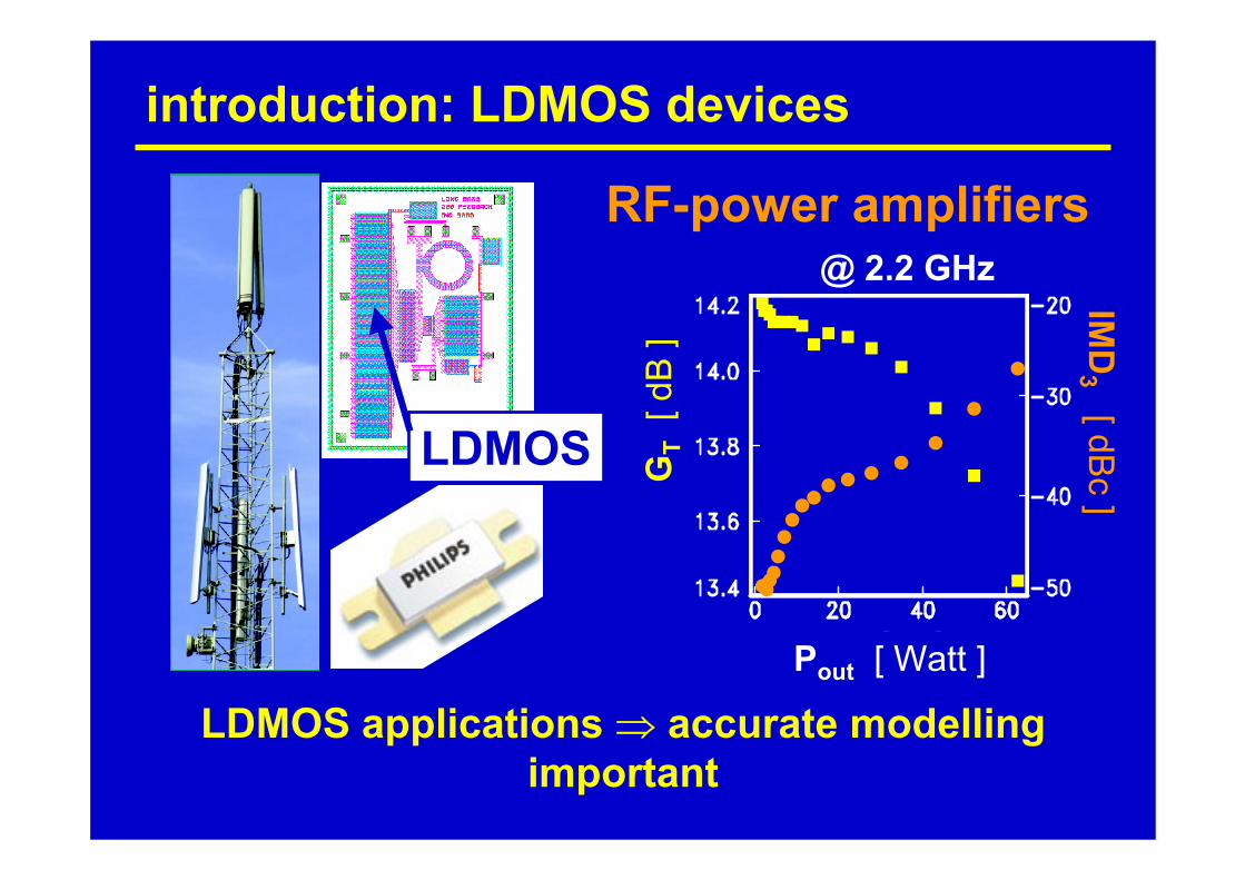
introduction: LDMOS devices
LDMOS applications ⇒ accurate modellingimportant
LDMOS
Pout [ Watt ]G
T[ d
B ]
IMD
3 [ dBc
]
@ 2.2 GHzRF-power amplifiers

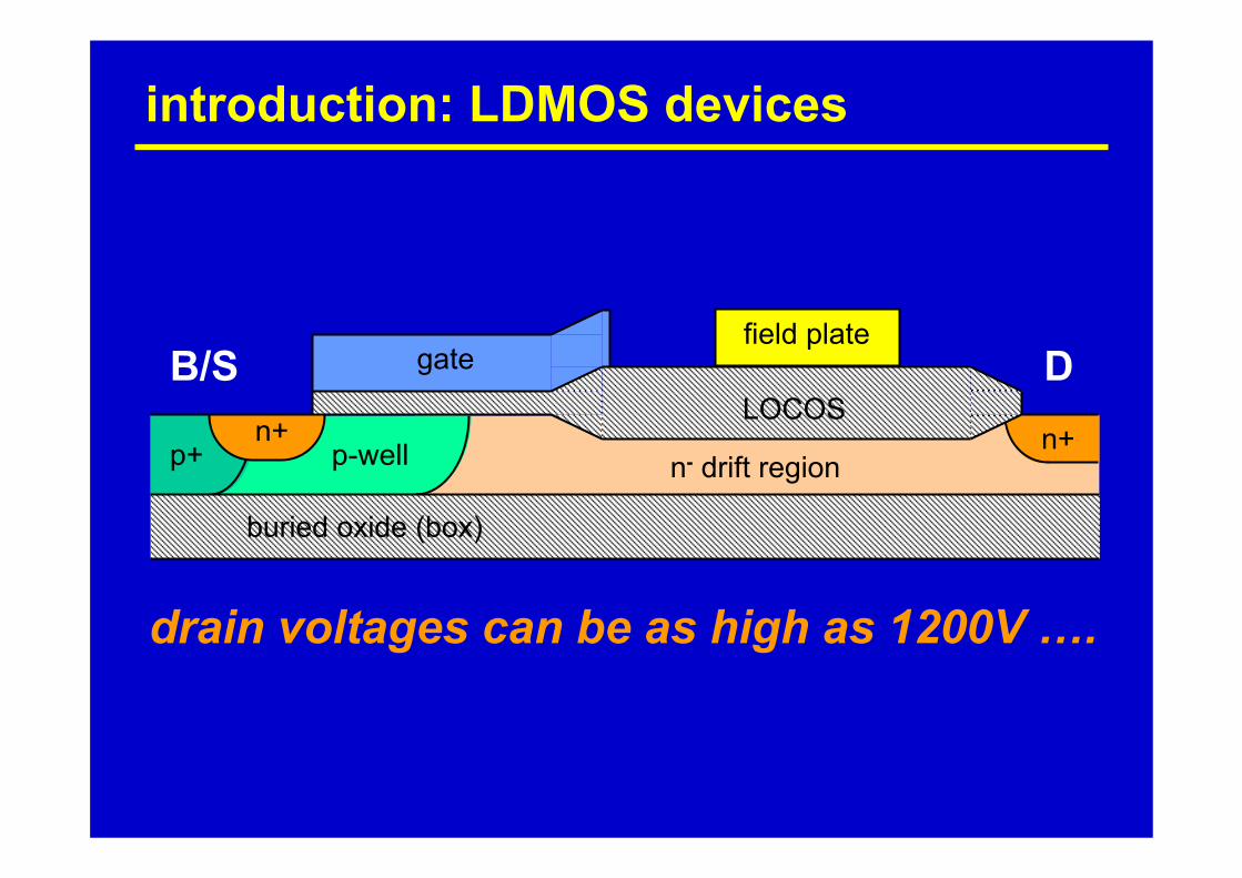
introduction: LDMOS devices
B/S D
buried oxide (box)
p-well n+p+ n- drift region
gate
n+LOCOS
to withstand high voltages
introduction: LDMOS devices
B/S D
buried oxide (box)
p-wellp+ n- drift region
gate
n+ n+LOCOS
field plate
drain voltages can be as high as 1200V ….

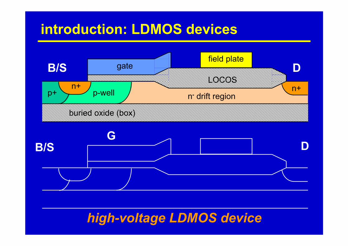
introduction: LDMOS devices
B/S D
buried oxide (box)
p-welln+
p+n- drift region
gate
n+
…. or drain voltages can be as low as 12V

introduction: LDMOS devices
B/S D
buried oxide (box)
p-wellp+ n- drift region
gate
n+ n+LOCOS
field plate
drain voltages vary between 12 and 1200V
B/S D
buried oxide (box)
p-well n+p+ n- drift region
gate
n+ LOCOS
B/S D
buried oxide (box)
p-well n+p+ n- drift region
gate
n+

introduction: LDMOS devices
B/S D
buried oxide (box)
p-welln+
p+n- drift region
gate
n+
B/S DG
low-voltage LDMOS device

introduction: LDMOS devices
B/S D
buried oxide (box)
p-welln+
p+n- drift region
gate
n+
B/S DGMM11 MM31
low-voltage LDMOS device

introduction: LDMOS devices
B/S D
buried oxide (box)
p-well n+p+ n- drift region
gate
n+LOCOS
medium-voltage LDMOS device
B/S DG

introduction: LDMOS devices
B/S D
buried oxide (box)
p-well n+p+ n- drift region
gate
n+LOCOS
medium-voltage LDMOS device
B/S DGMM11 MM31
introduction: LDMOS devices
B/S D
buried oxide (box)
p-wellp+ n- drift region
gate
n+ n+LOCOS
field plate
high-voltage LDMOS device
GB/S D

introduction: LDMOS devices
B/S D
buried oxide (box)
p-wellp+ n- drift region
gate
n+ n+LOCOS
field plate
B/S DG MM31MM11
high-voltage LDMOS device

outline
• introduction– LDMOS devices– modelling approaches
• MOS Model 20– basic model– additional model features
• summary

modelling approach: sub-circuit models
Gchannel region
DS
drift region
B

modelling approach: sub-circuit models
Gchannel region
DSMM31MM11
drift region
B
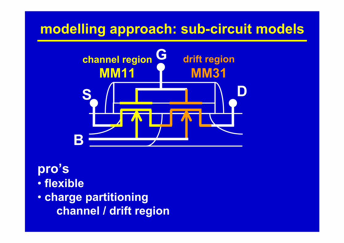
modelling approach: sub-circuit models
Gchannel region
DS
pro’s• flexible• charge partitioning
channel / drift region
MM31MM11drift region
B

modelling approach: sub-circuit models
Gchannel region
DS
pro’s• flexible• charge partitioning
channel / drift region
con’s• uncontrolled node• computation time /
convergence
MM31MM11drift region
B

modelling approach: single models
G
DS
B

modelling approach: single models
G
DS
B
MOS Model 20

modelling approach: single models
pro’s• no uncontrolled node • convergence
G
DS
B
MOS Model 20

modelling approach: single models
con’s• charge partitioning
channel / drift region
pro’s• no uncontrolled node • convergence
G
DS
B
MOS Model 20
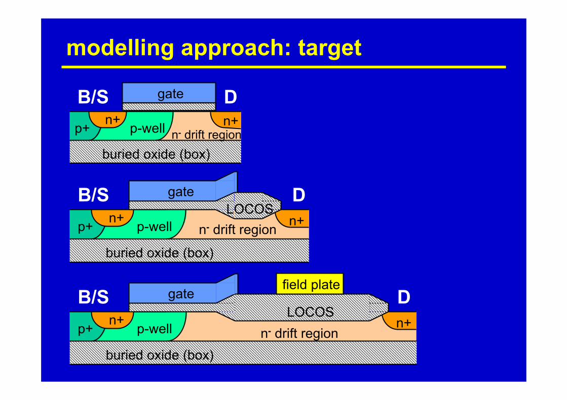
modelling approach: target
B/S D
buried oxide (box)
p-wellp+ n- drift region
gate
n+ n+LOCOS
field plate
B/S D
buried oxide (box)
p-well n+p+ n- drift region
gate
n+ LOCOS
B/S D
buried oxide (box)
p-well n+p+ n- drift region
gate
n+

modelling approach: target
B/S D
buried oxide (box)
p-wellp+ n- drift region
gate
n+ n+LOCOS
field plate
B/S D
buried oxide (box)
p-well n+p+ n- drift region
gate
n+ LOCOS
B/S D
buried oxide (box)
p-well n+p+ n- drift region
gate
n+B/S DGMM20
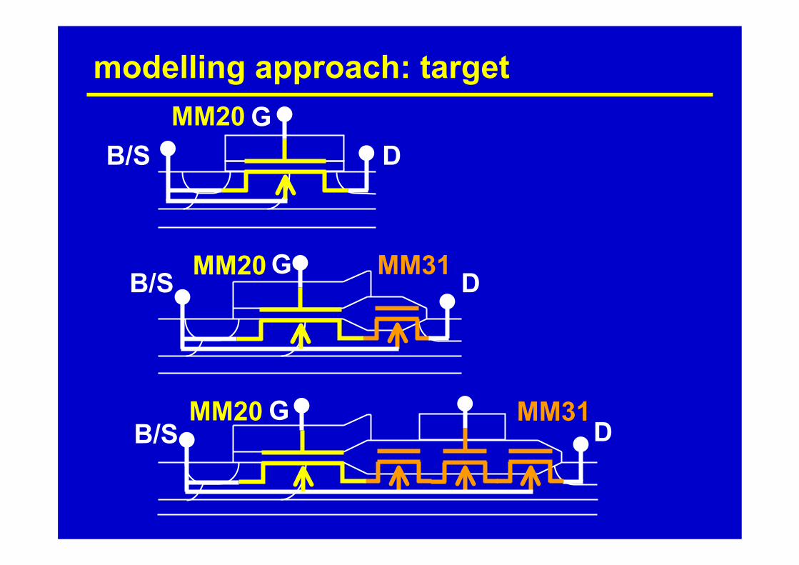
modelling approach: target
B/S DGMM20 MM31
B/S DGMM20
B/S DG MM31MM20

modelling approach: target
B/S DGMM20 MM31
B/S DGMM20
B/S DG MM31MM20
no such
thing as
“one model
fits all”
no such
thing as
“one model
fits all”

outline
• introduction• MOS Model 20
– basic model• DC-model• nodal charge model
– additional model features• summary

MOS Model 20: challenges
source
oxide
gate
drain
p-type n-type
drift region to withstand high voltages
channel region
lateral non-uniformity: 1. both p- and n-type 2. diffused p-well doping

MOS Model 20: DC-model
Kirchhoff’s current law (KCL): Ich = Idr
n+p
p+
B SG
Din+
n-
DIch Idr
1. determine VDi :
2. DC-current: IDS = Ich
approach:

essential to first determine VDi since
MOS Model 20: DC-model
n+p
p+
B SG
ψsLn+
n-
DIch Idr
IDS = Ich = Ich (ψsL, ψs0)ψsL = ψsL (VDiS, VGS, VSB )

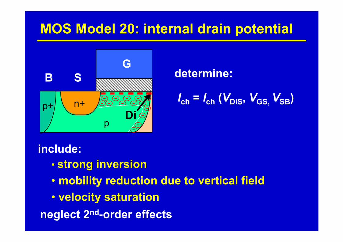
MOS Model 20: internal drain potential
Ich (VDiS, VGS, VSB) = Idr (VDDi, VGDi, VDiB)
n+p
p+
B SG
Din+
n-
DIch Idr
1. determine VDi from:
n+
p
p+
B SG
Din+
n-
D
• strong inversion• mobility reduction due to vertical field• velocity saturation
Ich = Ich (VDiS, VGS, VSB)
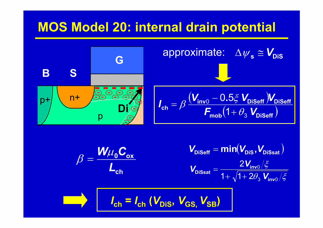
MOS Model 20: internal drain potential
determine:
include:
neglect 2nd-order effects

( )[ ]00 ssinvoxinv ψψξ −−−≅ VCQapproximation:
1501
0
0
++=
s
.ψ
ξ k
MOS Model 20: internal drain potential
n+
p
p+
B SG
Din+
n-
Dinclude strong inversion
∫ −=L
dQL
WIs
s
sinvch
chch
ψ
ψ
ψµ
0
inversion charge at source

( )[ ]00 ssinvoxinv ψψξ −−−≅ VCQapproximation:
1501
0
0
++=
s
.ψ
ξ k
MOS Model 20: internal drain potential
n+
p
p+
B SG
Din+
n-
Dinclude strong inversion
∫ −=L
dQL
WIs
s
sinvch
chch
ψ
ψ
ψµ
0
0sss ψψψ −=∆ L
ssinvch
oxchch ψψξµ
∆
∆−=
20VL
CWI
inversion charge at source

MOS Model 20: internal drain potential
Include:
n+
p
p+
B SG
Din+
n-
D• velocity saturation
s
effch ψθ
µµ∆+
=31
include
satch
0
vLµθ =3

• mobility reduction (surface scattering)
( ) mobs0s0inv0eff
SBFV V
0
021
0
1µ
ψψθθµµ =
−++=
=
MOS Model 20: internal drain potential
Include:
n+
p
p+
B SG
Din+
n-
D• velocity saturation
s
effch ψθ
µµ∆+
=31
include
satch
0
vLµθ =3
n+
p
p+
B SG
Din+
n-
D
ch
ox0
LCWµβ =
( )DiSsatDiSDiSeff ,min VVV =
ξθξ
03
0
2112
inv
invDiSsat V
VV++
=
MOS Model 20: internal drain potential
DiSs V≅∆ψapproximate:
( )( )DiSeffmob
DiSeffDiSeffinvch
.VF
VVVI3
0
150
θξβ+
−=
Ich = Ich (VDiS, VGS, VSB)

MOS Model 20: internal drain potential
Ich (VDiS, VGS, VSB) = Idr (VDDi, VGDi, VDiB)
n+p
p+
B SG
Din+
n-
DIch Idr
1. determine VDi from:

n+p
p+
B SG
n+
n-
DIch Idr
DiB
Idr = Idr (VDDi , VGDi , VDiB)
• accumulation• depletion• bulk current• mobility reduction due to vertical field• velocity saturation• pinch-off
MOS Model 20: internal drain potential
determine:
include:

n+p
p+
B SG
n+
n-
DIch Idr
DiB
∫ −=D
Di
Cdrn
dr
drdr
V
V
dVQL
WI µ
drdep
dracc
effSi
drn QQtqNQ D −−=
( )
−−−≅−≡
= DiCdr
noxdr
noxdrn
DiCVVVCVCQ
VV
bulk current
MOS Model 20: internal drain potential
approximation:
accumu-lation
depletion
n+p
p+
B SG
n+
n-
DIch Idr
DiB
DDidr
dreff
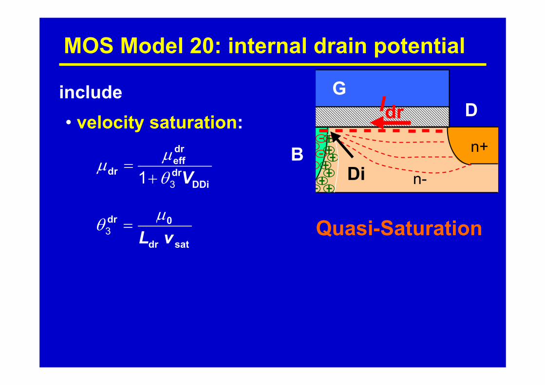
dr V31 θµµ
+=
• velocity saturation:
satdr
0dr
vLµθ =3 Quasi-Saturation
MOS Model 20: internal drain potential
include

n+p
p+
B SG
n+
n-
DIch Idr
DiB
DDidr
dreff
dr V31 θµµ
+=
• velocity saturation:
satdr
0dr
vLµθ =3
• mobility reduction (surface scattering):
( ) mobacc*
GD*
GSacc
dreff . FVV
0
1
0
501µ
θµµ =
++=
Quasi-Saturation
MOS Model 20: internal drain potential
include

n+p
p+
B SG
n+
n-
DIch Idr
Di
B
dr
ox0acc L
CWµβ =( )satDDi,DDieffDDi, ,min VVV =
DiC
DiC
drn
dr
drn
satDDi,
VV
VV
V
VV
=
=
++=
3211
2
θ
MOS Model 20: internal drain potential
Idr = Idr (VDDi, VGDi, VDiB)
( )effDDi,dr
mobacc
effDDi,effDDi,dr
n
accdr
.DiC
VF
VVVI VV
31
50
θβ
+
−
= =
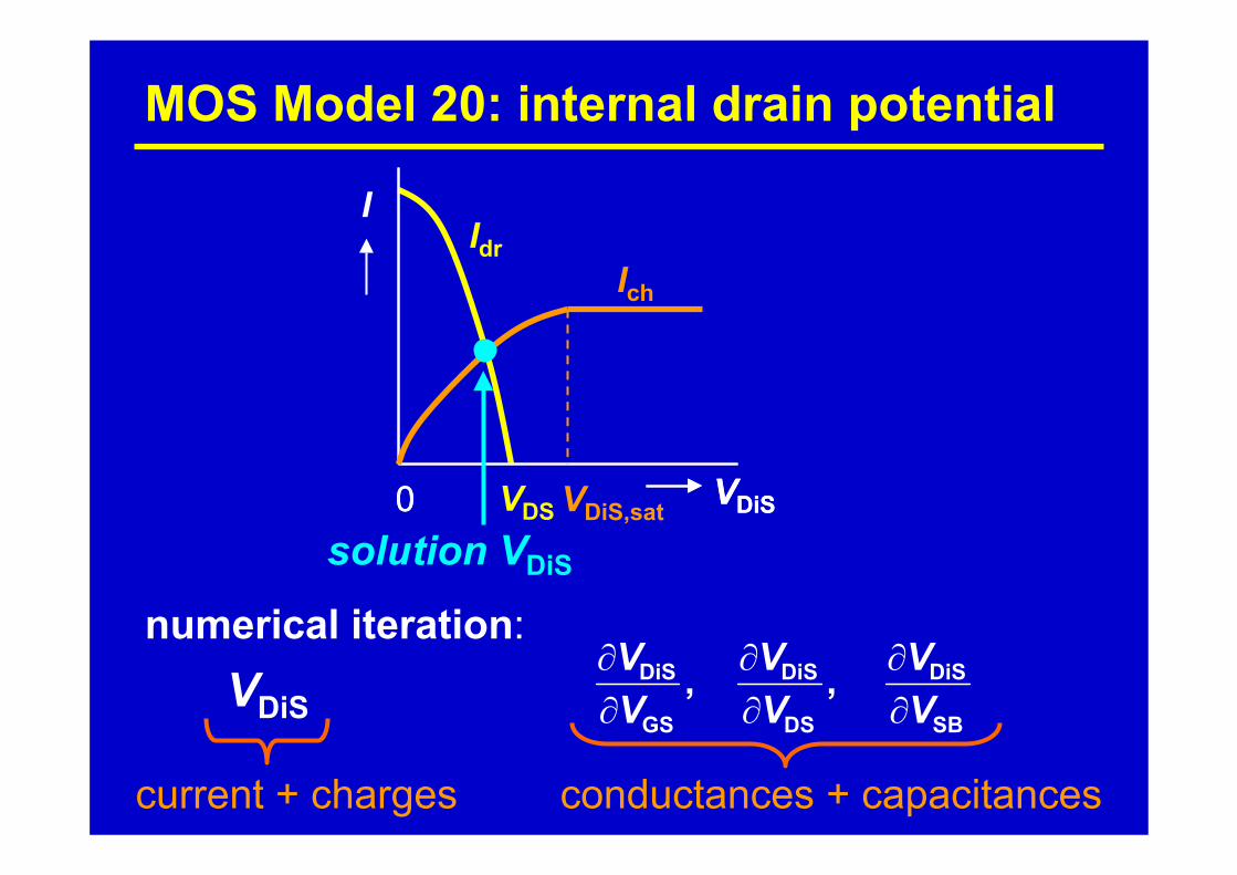
VDiS
numerical iteration:,
GS
DiS
VV
∂∂ ,
DS
DiS
VV
∂∂
SB
DiS
VV
∂∂
conductances + capacitances
0 VDS VDiS
Idr
0
I
VDiS,sat VDiS
Ich
solution VDiS
MOS Model 20: internal drain potential
current + charges

MOS Model 20: DC-model
Kirchhoff’s current law (KCL): Ich = Idr
n+p
p+
B SG
Din+
n-
DIch Idr
1. determine VDi :
2. DC-current: IDS = Ich
approach:

also include 2nd-order effects
MOS Model 20: DC-current
n+p
p+
B SG
ψsLn+
n-
DIch Idr
IDS = Ich (ψsL, ψs0)
ψsL = ψs (VSB + VDiSeff, VGB )ψs0 = ψs (VSB, VGB, )
surface-potential-based:

( )
−+−= ∫ 0
0
invinvsinvch
chDS
s
s
QQdQL
WI LT
L
φψµ ψ
ψ
MOS Model 20: DC-current
( )
( )smob∆
invinvssinv
DS
ψθ
φψψξ
β∆+
−+∆
∆−
=3
00
12
FG
VVVI
L
LT
( )( ) 2322
4
4/
DS
DSsfdibl,
VVDV
T
G+
=∆φ
• DIBL & static feedback:
• channel length modulation: ( )
−−=∆
P
DiSeffDS.
2ln1VVVG L α
drift diffusion
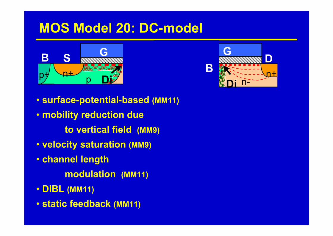
MOS Model 20: DC-model
• surface-potential-based (MM11)
• mobility reduction due to vertical field (MM9)
• velocity saturation (MM9)
• channel length modulation (MM11)
• DIBL (MM11)
• static feedback (MM11)
n+n-
Dn+ pp+
B S G
Di n+p
p+S
G
n+n-
D
DiB

MOS Model 20: DC-model
• surface-potential-based (MM11)
• mobility reduction due to vertical field (MM9)
• velocity saturation (MM9)
• channel length modulation (MM11)
• DIBL (MM11)
• static feedback (MM11)
n+n-
Dn+ pp+
B S G
Di
• accumulation• depletion• bulk current• mobility reduction due
to vertical field• velocity saturation
n+p
p+S
G
n+n-
D
DiB
outline
• introduction• MOS Model 20
– basic model• DC-model
– comparison with experimental data• nodal charge model
– additional model features• summary

MOS Model 20: experimental data
L = 1.6 µm12V SOI-LDMOS:
B/S D
buried oxide (box)
p-welln+
p+n- drift region
n+
G
L = Lch + Ldr + ∆L
low-voltage
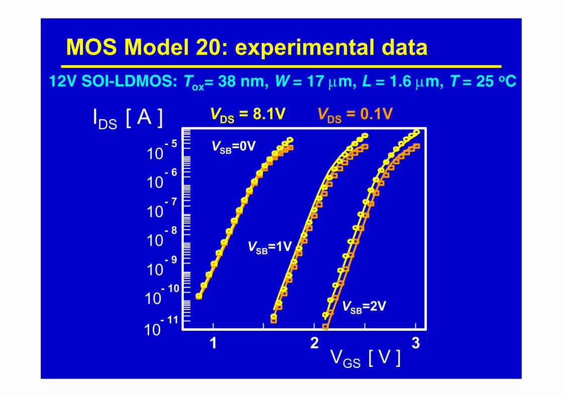
MOS Model 20: experimental data12V SOI-LDMOS: Tox= 38 nm, W = 17 µm, L = 1.6 µm, T = 25 oC
IDS [ A ] VDS = 8.1V VDS = 0.1V
VSB=0V
VSB=1V
VSB=2V
321VGS [ V ]
10- 11
10- 10
10- 9
10- 8
10- 7
10- 6
10- 5

MOS Model 20: experimental data
VSB = 0V
VSB = 1V
VSB = 2V
0 2 4 6 8 10 12VGS [ V ]
0
0.10.10.10.10.10.10.1
0.2
0.3
0.4IDS [ mA ]
VDS=0.1 V
12V SOI-LDMOS: Tox= 38 nm, W = 17 µm, L = 1.6 µm, T = 25 oC
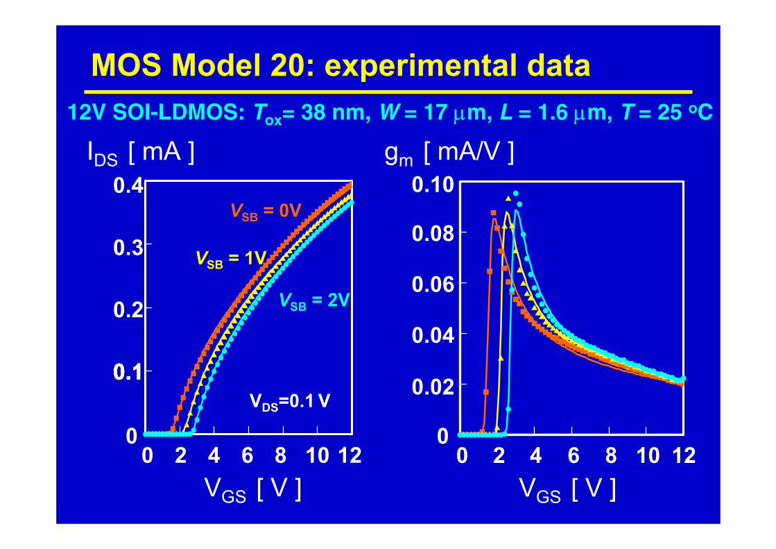
MOS Model 20: experimental data
0 2 4 6 8 10 12VGS [ V ]
0
0.02
0.04
0.06
0.08
0.10gm [ mA/V ]
VSB = 0V
VSB = 1V
VSB = 2V
0 2 4 6 8 10 12VGS [ V ]
0
0.10.10.10.10.10.10.1
0.2
0.3
0.4IDS [ mA ]
VDS=0.1 V
12V SOI-LDMOS: Tox= 38 nm, W = 17 µm, L = 1.6 µm, T = 25 oC

12V SOI-LDMOS: Tox= 38 nm, W = 17 µm, L = 1.6 µm, T = 25 oC
MOS Model 20: experimental data
VGS = VT + 2.1 V
VGS = VT + 3.1 V
VGS = VT + 1.1 V
VSB = 0VIDS [mA]
VDS [ V ]

MOS Model 20: experimental data12V SOI-LDMOS: Tox= 38 nm, W = 17 µm, L = 1.6 µm, T = 25 oC
2
4
6
8IDS [ mA ]
0 2 4 6 8 10VDS [ V ]
0
VGS = 6V
VGS = 12V
VGS = 9V
VGS = 3V
VSB=0 V
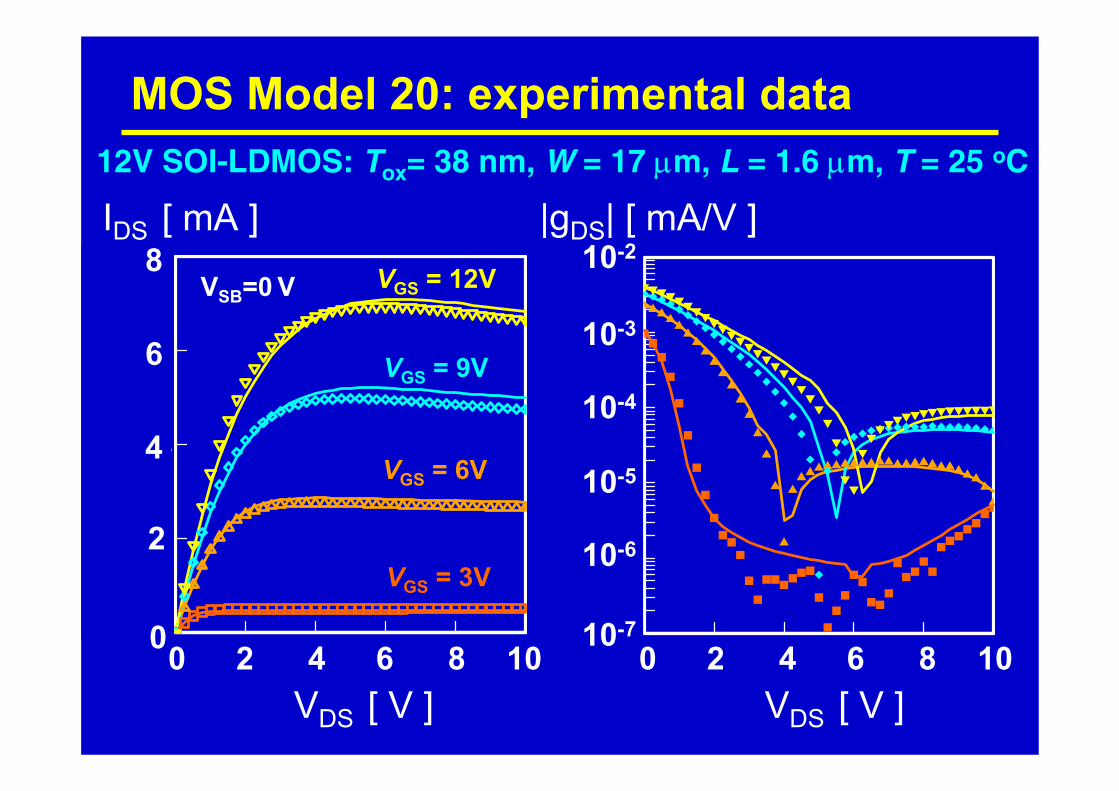
MOS Model 20: experimental data12V SOI-LDMOS: Tox= 38 nm, W = 17 µm, L = 1.6 µm, T = 25 oC
2
4
6
8IDS [ mA ]
0 2 4 6 8 10VDS [ V ]
0
VGS = 6V
VGS = 12V
VGS = 9V
VGS = 3V
VSB=0 V
0 2 4 6 8 10VDS [ V ]
10-7
10-6
10-5
10-4
10-3
10-2|gDS| [ mA/V ]

MOS Model 20: experimental data12V SOI-LDMOS: Tox= 38 nm, W = 17 µm, L = 1.6 µm, T = 25 oC
2
4
6
8IDS [ mA ]
0 2 4 6 8 10VDS [ V ]
0
VGS = 6V
VGS = 12V
VGS = 9V
VGS = 3V
VSB=0 V
0 2 4 6 8 10VDS [ V ]
10-7
10-6
10-5
10-4
10-3
10-2|gDS| [ mA/V ]
negative due to self-heating

VDS = 6V
VDS = 3V
VDS = 6V
VDS = 3V
VSB = 0V
12V SOI-LDMOS: Tox = 38 nm, W = 17 µm, L = 1.6 µm, T = 25 oC
MOS Model 20: experimental data
IDS [ mA ]
VGS [ V ]
gm [ mA/V ]
VGS [ V ]

MOS Model 20: quasi-saturation
sub-circuit
Tox = 38 nm, L = 2.6 µm, LLOCOS = 3.5 µm
high-voltageB/S D
buried oxide (box)
p-well n+p+ n- drift region
gate
n+LOCOS
L LLOCOS
60V SOI-LDMOS:
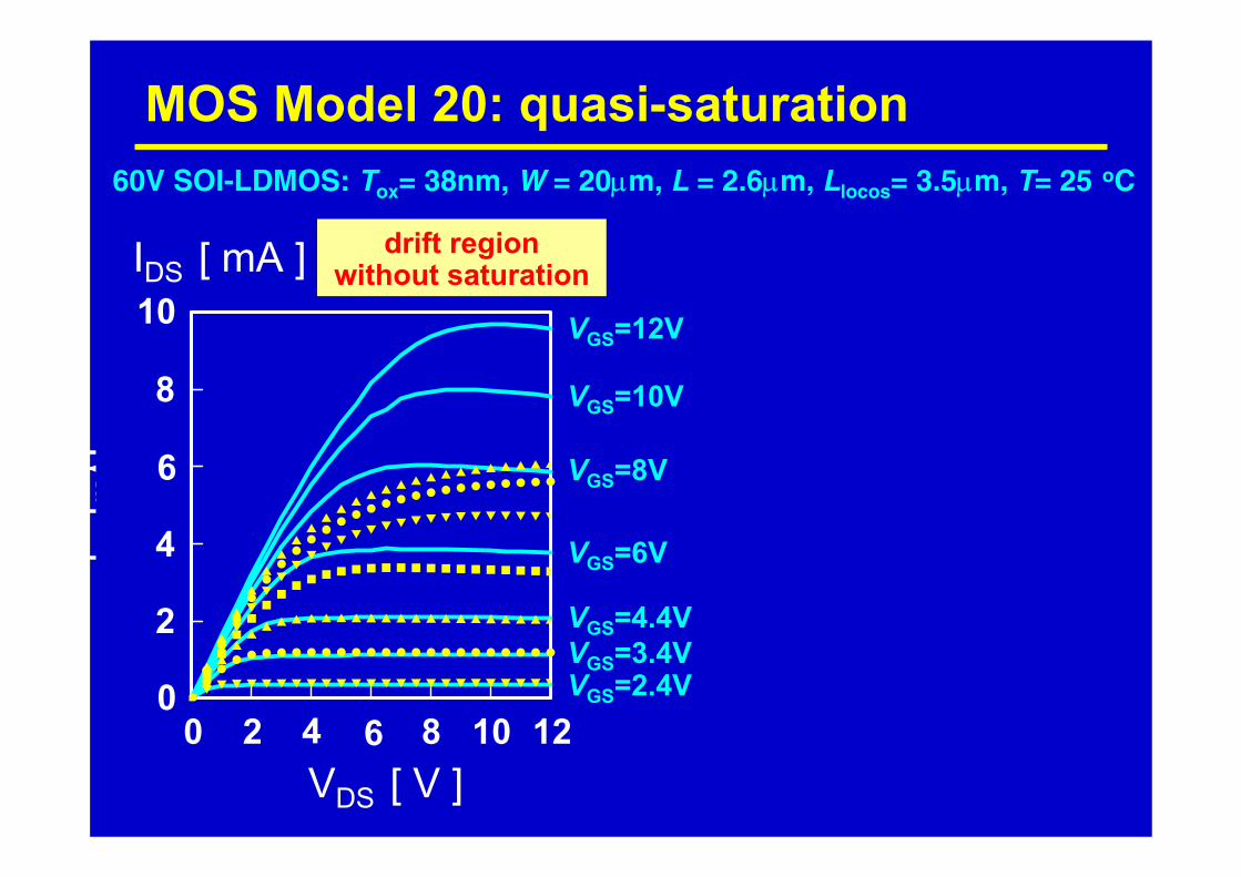
60V SOI-LDMOS: Tox= 38nm, W = 20µm, L = 2.6µm, Llocos= 3.5µm, T= 25 oC
IDS [ mA ]10
8
6
4
0
2
2 6 8 12VDS [ V ]
0 4 10
drift region without saturation
VGS=2.4VVGS=3.4VVGS=4.4V
VGS=6V
VGS=8V
VGS=10V
VGS=12V
MOS Model 20: quasi-saturation

60V SOI-LDMOS: Tox= 38nm, W = 20µm, L = 2.6µm, Llocos= 3.5µm, T= 25 oC
IDS [ mA ]10
8
6
4
0
2
2 6 8 12VDS [ V ]
0 4 10
IDS [ mA ]10
8
6
4
0
2
2 6 8 12VDS [ V ]
0 4 10
drift region without saturation
drift region with saturation
VGS=2.4VVGS=3.4VVGS=4.4V
VGS=6V
VGS=8V
VGS=10V
VGS=12V
MOS Model 20: quasi-saturation
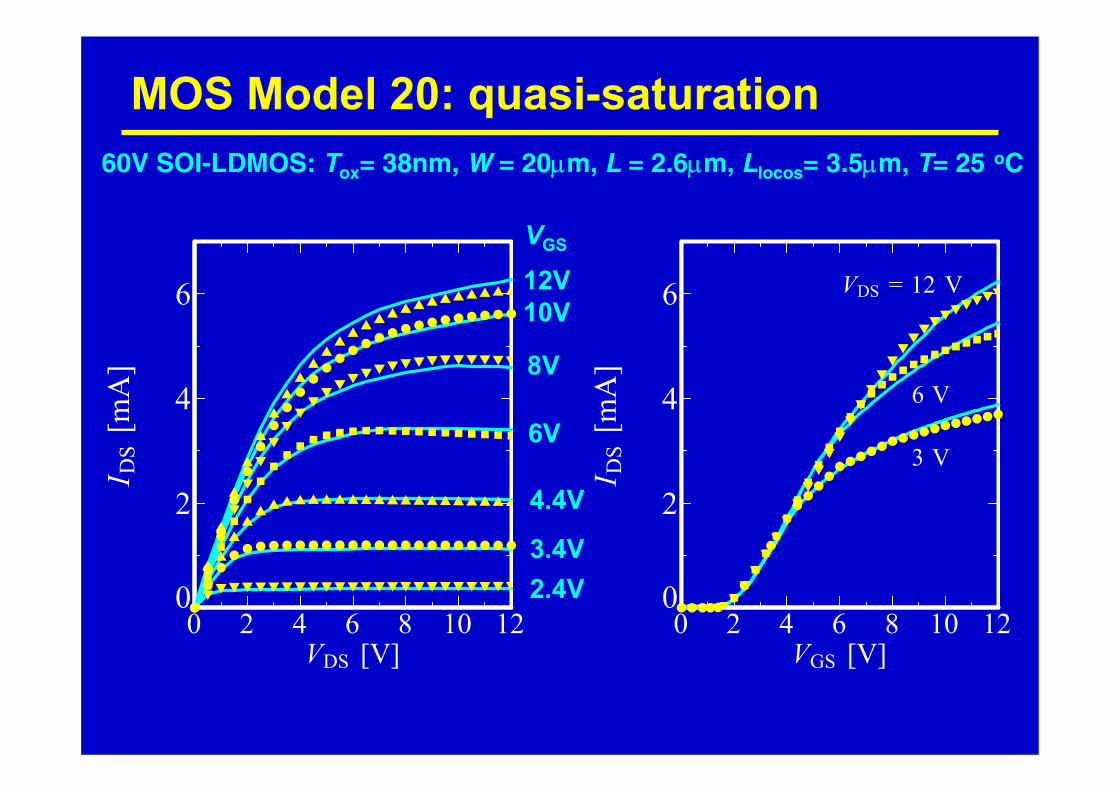
60V SOI-LDMOS: Tox= 38nm, W = 20µm, L = 2.6µm, Llocos= 3.5µm, T= 25 oC
MOS Model 20: quasi-saturation
0 2 4 6 8 10 120
2
4
6
V GS [V] I D
S[m
A]
6 V
V DS = 12 V
3 V
0 2 4 6 8 10 120
2
4
6
V DS [V]
I DS
[mA
]
2.4V3.4V
4.4V
6V
8V
10V12VVGS
60V SOI-LDMOS: Tox= 38nm, W = 20µm, L = 2.6µm, Llocos= 3.5µm, T= 25 oC
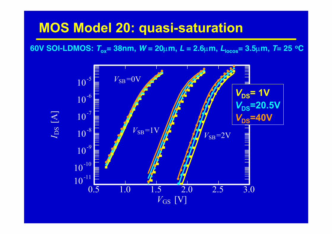
MOS Model 20: quasi-saturation
0.5 1.0 1.5 2.0 2.5 3.0 10-11 10-10
10-9
10-8
10-7
10-6
10-5
V GS [V]
I DS
[A]
V SB =0V
V SB =1V V SB=2V
VDS= 1VVDS=20.5VVDS=40V

outline
• introduction• MOS Model 20
– basic model• DC-model• nodal charge model
– additional model features• summary
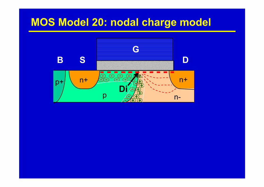
MOS Model 20: nodal charge model
n+
p
p+
B SG
Din+
n-
D

MOS Model 20: gate and bulk charges
( )∫ ⋅++−=L
dxQQQWQ0
'acc
'dep
'invchannel G,
( )∫ ⋅+=L
dxQQWQ0
'acc
'depchannel B,
n+
p
p+
B SG
Din+
n-
D
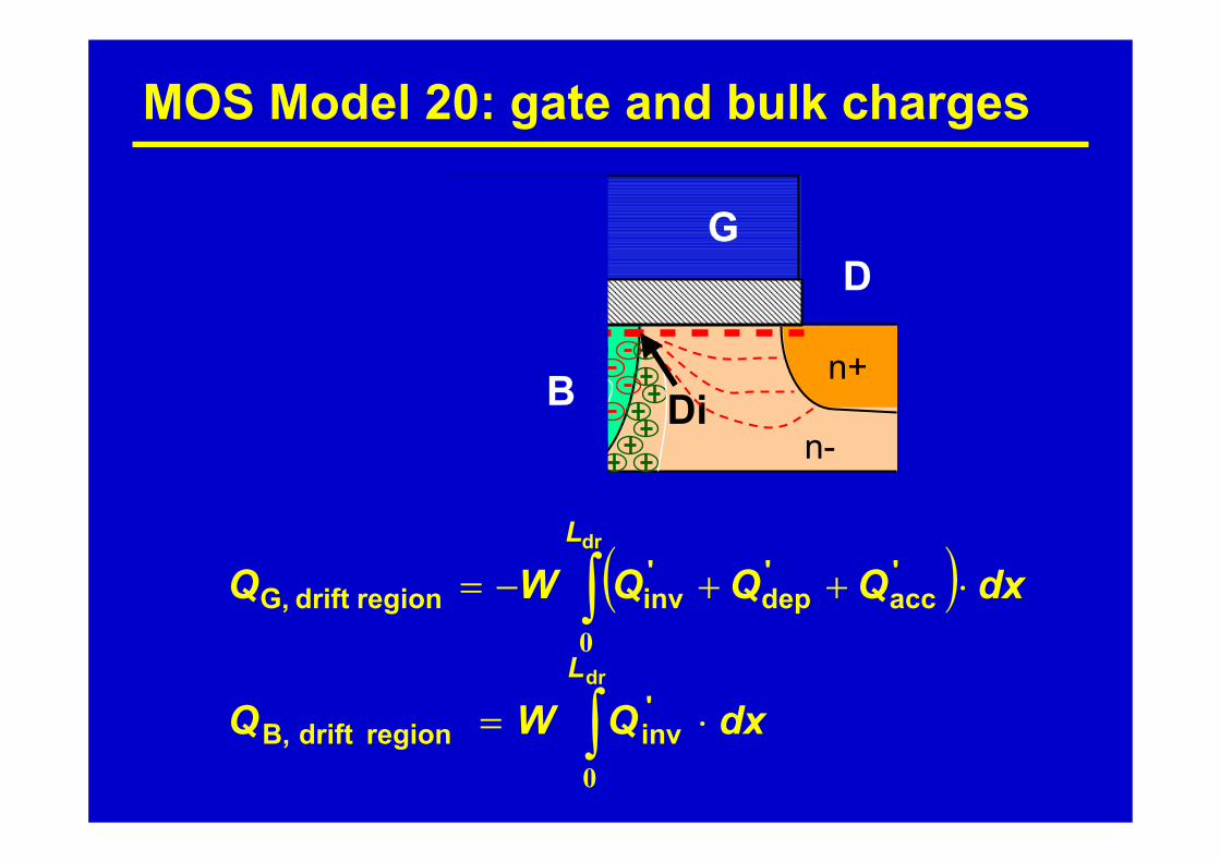
( )∫ ⋅++−=dr
'acc
'dep
'invregiondrift G,
L
dxQQQWQ0
∫ ⋅=dr
'invregiondrift B,
L
dxQWQ0
MOS Model 20: gate and bulk charges
n+
p
p+
SG
Din+
n-
D
B

regiondrift G,channel G,LDMOS G, QQQ +=
regiondrift B,channel B,LDMOS B, QQQ +=
MOS Model 20: gate and bulk charges
n+
p
p+
B SG
Din+
n-
D

regiondrift G,channel G,LDMOS G, QQQ +=
regiondrift B,channel B,LDMOS B, QQQ +=( )
j
iijij 12
VQC
∂∂
⋅−⋅= δ
MOS Model 20: gate and bulk charges
n+
p
p+
B SG
Din+
n-
D

outline
• introduction• MOS Model 20
– basic model• DC-model• nodal charge model
– comparison with experimental data– additional model features
• summary

MOS Model 20: experimental data14V SOI-LDMOS: Tox = 60 nm, W = 50 µm, L = 5 µm, T = 25 oC
-5 0 5 10
100
150
200
V GS [V]
C GG
[fF]
V DS = 5V1V
0V

MOS Model 20: experimental data14V SOI-LDMOS: Tox = 60 nm, W = 50 µm, L = 5 µm, T = 25 oC
-5 0 5 10
100
150
200
V GS [V]
C GG
[fF]
V DS = 5V1V
0V
0 5 10
150
200
!5V!DGS!N!5=9V
V DS [V]
C GG
[fF]
V GS = 9V
V GS = 5V

MOS Model 20: experimental data14V SOI-LDMOS: Tox = 60 nm, W = 50 µm, L = 5 µm, T = 25 oC
-5 0 5 100
50
100
150
V GS [V]
C GD
[fF]
V DS = 0V
V DS = 5V
V DS = 14V

MOS Model 20: experimental data14V SOI-LDMOS: Tox = 60 nm, W = 50 µm, L = 5 µm, T = 25 oC
-5 0 5 100
50
100
150
V GS [V]
C GD
[fF]
V DS = 0V
V DS = 5V
V DS = 14V
0 5 100
50
100
150
V DS [V]
C GD
[fF]
V GS = 9V
V GS = 5V

outline
• introduction• MOS Model 20
– basic model• DC-model• nodal charge model
– additional model features• summary
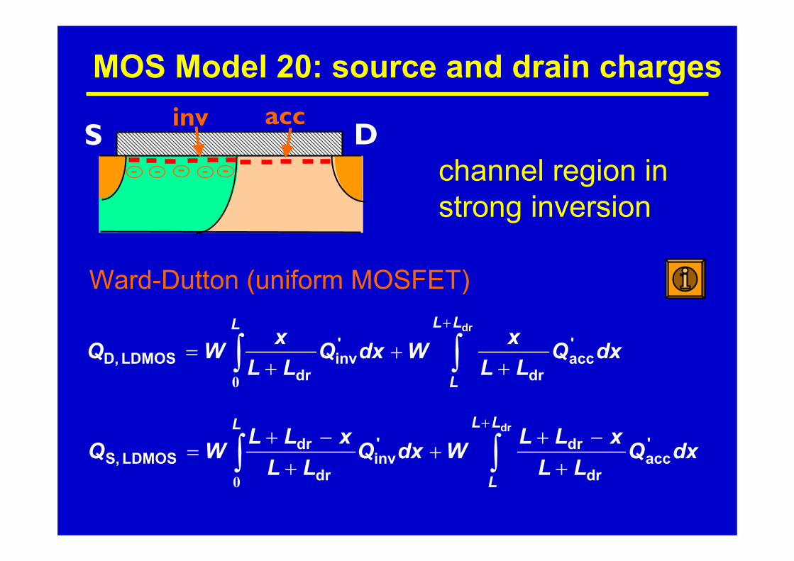
MOS Model 20: source and drain chargesaccinv
S D
∫ ∫+
++
+=
L LL
L
dxQLL
xWdxQLL
xWQ0
dr'acc
dr
'inv
drLDMOS D,
∫ ∫+
+−+
++
−+=
L LL
L
dxQLL
xLLWdxQLL
xLLWQ0
dr'acc
dr
dr'inv
dr
drLDMOS S,
Ward-Dutton (uniform MOSFET)
channel region instrong inversion

MOS Model 20: source and drain charges
∫+
=dr
'accLDMOS D,
LL
L
dxQWQ
S Dacc
channel region inweak inversion
0=LDMOS S,Q
all charge in the drift region attributed to the drain
outline
• introduction• MOS Model 20
– basic model• DC-model• nodal charge model
– comparison with experimental data– additional model features
• summary
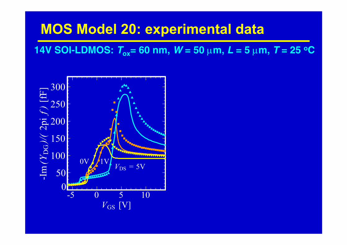
-5 0 5 100
50
100
150
200
250
300
V GS [V]
-Im
( Y DG
)/( 2
pi f
) [f
F]
V DS = 5V1V0V
MOS Model 20: experimental data14V SOI-LDMOS: Tox= 60 nm, W = 50 µm, L = 5 µm, T = 25 oC

-5 0 5 100
50
100
150
200
250
300
V GS [V]
-Im
( Y DG
)/( 2
pi f
) [f
F]
V DS = 5V1V0V
MOS Model 20: experimental data14V SOI-LDMOS: Tox= 60 nm, W = 50 µm, L = 5 µm, T = 25 oC
0 5 10
100
150
200
250
300
350
V DS [V]
-Im
( Y DG
)/( 2
pi f
) [f
F] V GS = 5V
V GS = 7V
V GS = 9V
MOS Model 20: experimental data14V SOI-LDMOS: Tox= 60 nm, W = 50 µm, L = 5 µm, T = 25 oC
-5 0 5 100
50
100
150
200
V GS [V]
Im( Y
DD)/(
2pi
f )
[fF] V DS = 0V
1V
5V
14V

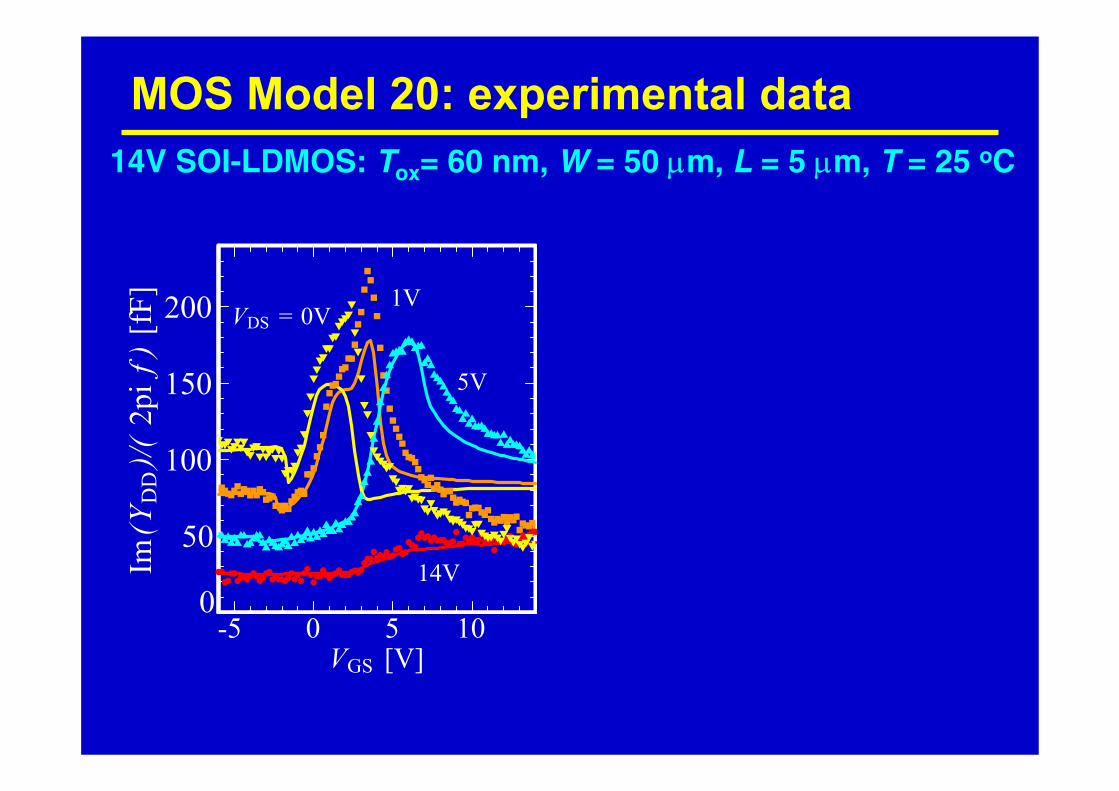
MOS Model 20: experimental data14V SOI-LDMOS: Tox= 60 nm, W = 50 µm, L = 5 µm, T = 25 oC
-5 0 5 100
50
100
150
200
V GS [V]
Im( Y
DD)/(
2pi
f )
[fF] V DS = 0V
1V
5V
14V
0 5 100
50
100
150
200
250
V DS [V]
Im( Y
DD)/(
2pi
f )
[fF] V GS = 9V
V GS = 5V
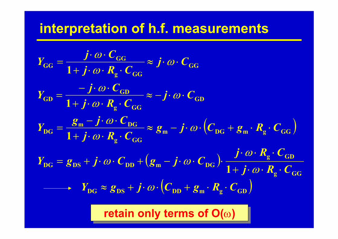
interpretation of h.f. measurements
GGGGg
GGGG 1
CjCRj
CjY ⋅⋅≈⋅⋅⋅+
⋅⋅= ω
ωω
GDGGg
GDGD 1
CjCRj
CjY ⋅⋅−≈⋅⋅⋅+
⋅⋅−= ω
ωω
( )GGgmDGmGGg
DGmDG 1
CRgCjgCRjCjgY ⋅⋅+⋅⋅−≈⋅⋅⋅+
⋅⋅−= ω
ωω
( )GGg
GDgDGmDDDSDG 1 CRj
CRjCjgCjgY
⋅⋅⋅+
⋅⋅⋅⋅⋅⋅−+⋅⋅+=
ωω
ωω
( )GDgmDDDSDG CRgCjgY ⋅⋅+⋅⋅+≈ ω
retain only terms of O(ω)retain only terms of O(ω)
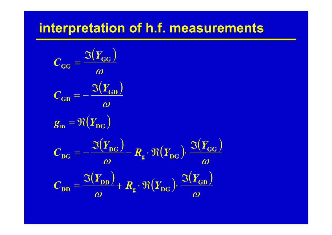
interpretation of h.f. measurements
( )ωGG
GGYC ℑ
=
( )ωGD
GDYC ℑ
−=
( ) ( ) ( )ωωGG
DGgDG
DGYYRYC ℑ
⋅ℜ⋅−ℑ
−=
( ) ( ) ( )ωωGD
DGgDD
DDYYRYC ℑ
⋅ℜ⋅+ℑ
=
( )DGm Yg ℜ=
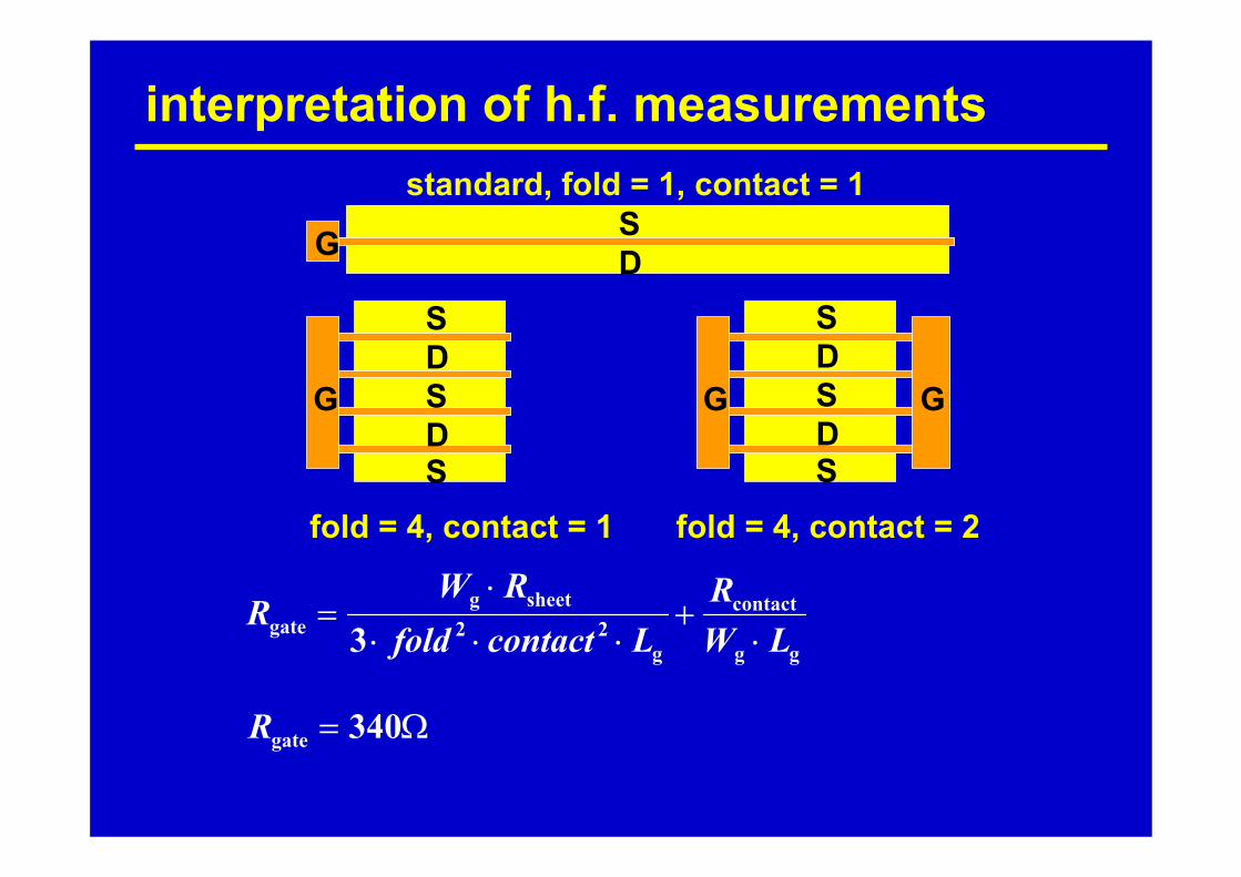
interpretation of h.f. measurements
gg
contact
g22
sheetggate 3 LW
RLcontactfold
RWR
⋅+
⋅⋅⋅
⋅=
standard, fold = 1, contact = 1
fold = 4, contact = 1 fold = 4, contact = 2
G G G
G
SDSDS
SDSDS
SD
Ω= 340gateR

MOS Model 20: experimental data14V SOI-LDMOS: Tox= 60 nm, W = 50 µm, L = 5 µm, T = 25 oC
-5 0 5 100
50
100
150
200
V GS [V]
C DG
[fF]
V DS = 5V1V0V
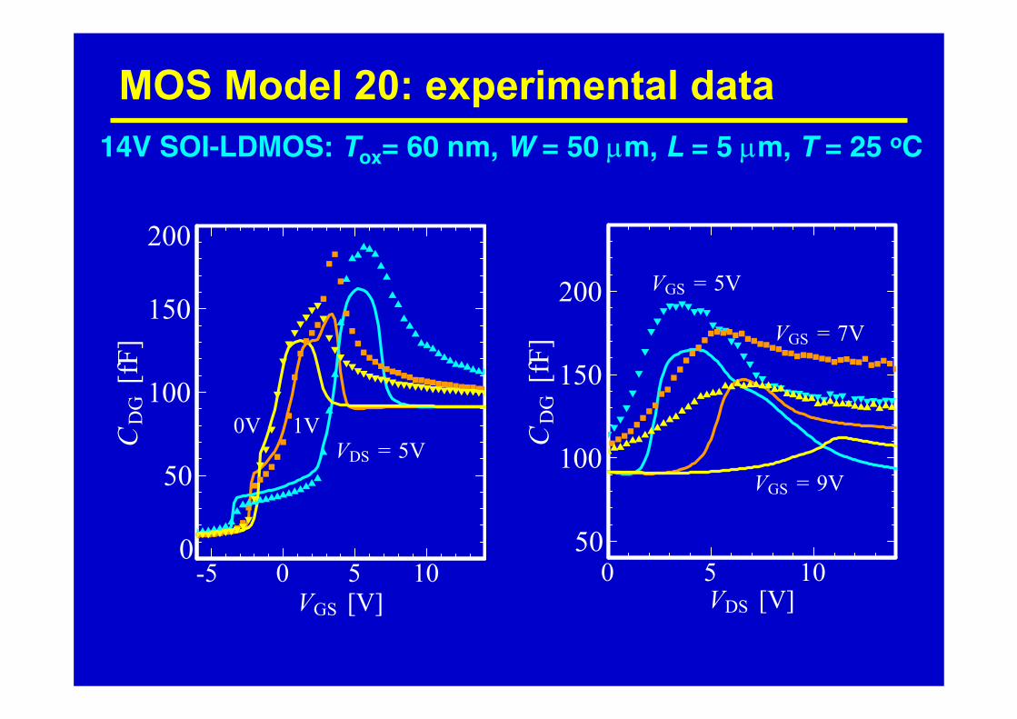
MOS Model 20: experimental data14V SOI-LDMOS: Tox= 60 nm, W = 50 µm, L = 5 µm, T = 25 oC
-5 0 5 100
50
100
150
200
V GS [V]
C DG
[fF]
V DS = 5V1V0V
0 5 1050
100
150
200
V DS [V]
C DG
[fF]
V GS = 5V
V GS = 7V
V GS = 9V
MOS Model 20: experimental data14V SOI-LDMOS: Tox= 60 nm, W = 50 µm, L = 5 µm, T = 25 oC
-5 0 5 100
50
100
150
200
V GS [V]
C DD
[fF]
V DS = 0V
1V
5V
14V

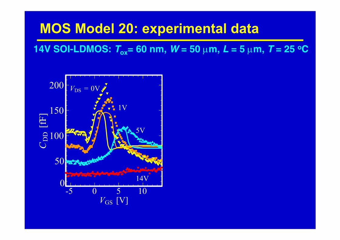
MOS Model 20: experimental data14V SOI-LDMOS: Tox= 60 nm, W = 50 µm, L = 5 µm, T = 25 oC
-5 0 5 100
50
100
150
200
V GS [V]
C DD
[fF]
V DS = 0V
1V
5V
14V
0 5 100
50
100
150
V DS [V]
C DD
[fF]
V GS = 9V
V GS = 5V

MOS Model 20: experimental data14V SOI-LDMOS: Tox= 60 nm, W = 50 µm, L = 5 µm, T = 25 oC
VGS [ V ]3 6 9 120
VDS = 5V
VDS = 14V
VDS = 1V
fT [ GHz ]2.0
1.5
1.0
0.5
0
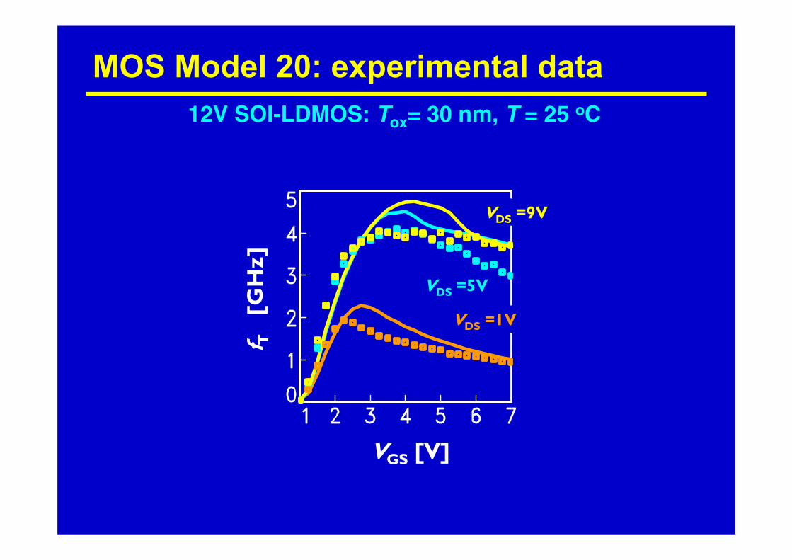
VGS [V]
f T[G
Hz]
VDS =9V
VDS =1V
VDS =5V
MOS Model 20: experimental data12V SOI-LDMOS: Tox= 30 nm, T = 25 oC

outline
• introduction• MOS Model 20
– basic model– additional model features
• parameters• self-heating and temperature scaling• geometry scaling• bulk current• noise
• summary

parameters of electrical modelmeaningparameterno.
exponent of weak avalanche current A236temperature scaling coefficient for A1STA135factor of weak-avalanche current at ref. temp. A134
gate-source overlap capacitanceCGSO41gate-drain overlap capacitanceCGDO40oxide capacitance for intrinsic drift regionCOXD39oxide capcitance for intrinsic channel regionCOX38
factor of drain-source voltage above which weak avalanche occurs
A337
factor for static feedbackSSF33parameter for subthreshold slopeMO32exponent for DIBL dependence on back biasMSDIBL31factor for drain-induced barrier-loweringSDIBL30
parameters of electrical modelmeaningparameterno.channel mobility reduction coefficient due to vertical field caused by depletion
THE221
char. voltage of channel length modulationVP29factor for channel length modulationALP28drift region: trans. from linear to sat. regimeMEXPD27drift region: temperature scaling exponentETATHE3D26
THE3D25transition from linear to saturation regimeMEXP24temperature scaling exponentETATHE323
channel mobility reduction coefficient due to horizontal field
THE322
drift region: channel mobility reduction coefficient due to horizontal field
parameters of electrical model
drift region mobility reduction coefficient due to vertical field caused by accumulation
THE1ACC20
channel mobility reduction coefficient due to vertical field caused by strong inversion
THE119
quotient of depletion layer thickness at VSB>0, to effective thickness of drift region at VSB=0
LAMD18temperature scaling exponentETARD17on-resistance of drift region at reference temp.RD16temperature scaling exponentETABETACC15
accumulation gain factor in drift region at reference temp.
BETACC14temperature scaling exponentETABET13gain factor of channel region at reference temp.BET12meaningparameterno.
surface potential at onset of strong inversion in drift region at reference temperature
PHIBD10
temperature scaling coefficientSTPHIBD11
temperature scaling coefficientSTPHIB9
surface potential at onset of strong inversion in channel region at reference temperature
PHIB8body factor of drift regionKOD7body factor of channel regionKO6temperature scaling coefficientSTVFBD5flatband voltage of drift region at ref. temp.VFBD4temperature scaling coefficientSTVFB3flatband voltage of channel at reference temp.VFB2reference temperatureTREF12002LEVEL0meaningparameterno.
parameters of electrical model
MOS Model 20: parameters
• 24 DC parameters
parameters of electrical modelmeaningparameterno.
number of devices in parallel MULT48temperature offset to ambient temperatureDTA47thickness of oxide above channel regionTOX46third coefficient of flicker noiseNFC45second coefficient of flicker noiseNFB44first coefficient of flicker noiseNFA43coefficient of thermal noise at ref. temperatureNT42

parameters of electrical modelmeaningparameterno.
exponent of weak avalanche current A236temperature scaling coefficient for A1STA135factor of weak-avalanche current at ref. temp. A134
gate-source overlap capacitanceCGSO41gate-drain overlap capacitanceCGDO40oxide capacitance for intrinsic drift regionCOXD39oxide capcitance for intrinsic channel regionCOX38
factor of drain-source voltage above which weak avalanche occurs
A337
factor for static feedbackSSF33parameter for subthreshold slopeMO32exponent for DIBL dependence on back biasMSDIBL31factor for drain-induced barrier-loweringSDIBL30
parameters of electrical modelmeaningparameterno.channel mobility reduction coefficient due to vertical field caused by depletion
THE221
char. voltage of channel length modulationVP29factor for channel length modulationALP28drift region: trans. from linear to sat. regimeMEXPD27drift region: temperature scaling exponentETATHE3D26
THE3D25transition from linear to saturation regimeMEXP24temperature scaling exponentETATHE323
channel mobility reduction coefficient due to horizontal field
THE322
drift region: channel mobility reduction coefficient due to horizontal field
parameters of electrical model
drift region mobility reduction coefficient due to vertical field caused by accumulation
THE1ACC20
channel mobility reduction coefficient due to vertical field caused by strong inversion
THE119
quotient of depletion layer thickness at VSB>0, to effective thickness of drift region at VSB=0
LAMD18temperature scaling exponentETARD17on-resistance of drift region at reference temp.RD16temperature scaling exponentETABETACC15
accumulation gain factor in drift region at reference temp.
BETACC14temperature scaling exponentETABET13gain factor of channel region at reference temp.BET12meaningparameterno.
surface potential at onset of strong inversion in drift region at reference temperature
PHIBD10
temperature scaling coefficientSTPHIBD11
temperature scaling coefficientSTPHIB9
surface potential at onset of strong inversion in channel region at reference temperature
PHIB8body factor of drift regionKOD7body factor of channel regionKO6temperature scaling coefficientSTVFBD5flatband voltage of drift region at ref. temp.VFBD4temperature scaling coefficientSTVFB3flatband voltage of channel at reference temp.VFB2reference temperatureTREF12002LEVEL0meaningparameterno.
parameters of electrical model
MOS Model 20: parameters
• 24 DC parameters • temperature scaling
• 6 parameters
parameters of electrical modelmeaningparameterno.
number of devices in parallel MULT48temperature offset to ambient temperatureDTA47thickness of oxide above channel regionTOX46third coefficient of flicker noiseNFC45second coefficient of flicker noiseNFB44first coefficient of flicker noiseNFA43coefficient of thermal noise at ref. temperatureNT42

parameters of electrical modelmeaningparameterno.
exponent of weak avalanche current A236temperature scaling coefficient for A1STA135factor of weak-avalanche current at ref. temp. A134
gate-source overlap capacitanceCGSO41gate-drain overlap capacitanceCGDO40oxide capacitance for intrinsic drift regionCOXD39oxide capcitance for intrinsic channel regionCOX38
factor of drain-source voltage above which weak avalanche occurs
A337
factor for static feedbackSSF33parameter for subthreshold slopeMO32exponent for DIBL dependence on back biasMSDIBL31factor for drain-induced barrier-loweringSDIBL30
parameters of electrical modelmeaningparameterno.channel mobility reduction coefficient due to vertical field caused by depletion
THE221
char. voltage of channel length modulationVP29factor for channel length modulationALP28drift region: trans. from linear to sat. regimeMEXPD27drift region: temperature scaling exponentETATHE3D26
THE3D25transition from linear to saturation regimeMEXP24temperature scaling exponentETATHE323
channel mobility reduction coefficient due to horizontal field
THE322
drift region: channel mobility reduction coefficient due to horizontal field
parameters of electrical model
drift region mobility reduction coefficient due to vertical field caused by accumulation
THE1ACC20
channel mobility reduction coefficient due to vertical field caused by strong inversion
THE119
quotient of depletion layer thickness at VSB>0, to effective thickness of drift region at VSB=0
LAMD18temperature scaling exponentETARD17on-resistance of drift region at reference temp.RD16temperature scaling exponentETABETACC15
accumulation gain factor in drift region at reference temp.
BETACC14temperature scaling exponentETABET13gain factor of channel region at reference temp.BET12meaningparameterno.
surface potential at onset of strong inversion in drift region at reference temperature
PHIBD10
temperature scaling coefficientSTPHIBD11
temperature scaling coefficientSTPHIB9
surface potential at onset of strong inversion in channel region at reference temperature
PHIB8body factor of drift regionKOD7body factor of channel regionKO6temperature scaling coefficientSTVFBD5flatband voltage of drift region at ref. temp.VFBD4temperature scaling coefficientSTVFB3flatband voltage of channel at reference temp.VFB2reference temperatureTREF12002LEVEL0meaningparameterno.
parameters of electrical model
MOS Model 20: parameters
• 24 DC parameters • temperature scaling
• 6 parameters• width scaling
• 7 parametersparameters of electrical model
meaningparameterno.
number of devices in parallel MULT48temperature offset to ambient temperatureDTA47thickness of oxide above channel regionTOX46third coefficient of flicker noiseNFC45second coefficient of flicker noiseNFB44first coefficient of flicker noiseNFA43coefficient of thermal noise at ref. temperatureNT42

outline
• introduction• MOS Model 20
– basic model– additional model features
• parameters• self-heating and temperature scaling• geometry scaling• bulk current• noise
• summary

MOS Model 20: self-heating• self-heating network inside model:
• temperature-dependent model parameters
• derivatives w.r.t. temperature (ac and transient)
PdissR th
∆T
C th

θ3
βacc
β
1/ RD
βacc [mA/V2]
β [mA/V2] θ3 [1/V]
1/ RD [mA/V]
temperature T [K]
MOS Model 20: temperature scaling
0.3
0.5
0.4
0.2400300
3
1
0.3

T = 125 oCT = 10 oC
MOS Model 20: temperature scaling
IDS [mA] IDS [mA]
VGS = 3V
VGS = 6V
VGS = 9VVGS = 12V
VGS = 3V
VGS = 6V
VGS = 9V
VGS = 12V
12V SOI-LDMOS: Tox = 38 nm, W = 17 µm, L = 1.6 µm
VDS (V) VDS (V)
outline
• introduction• MOS Model 20
– basic model– additional model features
• parameters• self-heating and temperature scaling• geometry scaling• bulk current• noise
• summary

MOS Model 20: width scaling
0 20 40 600
2
4
6
W mask [ µ m]
1 / R D [mA/V]
[mA/V 2 ]
[mA/V 2 ]
β
ββ acc
β acc
1/RD
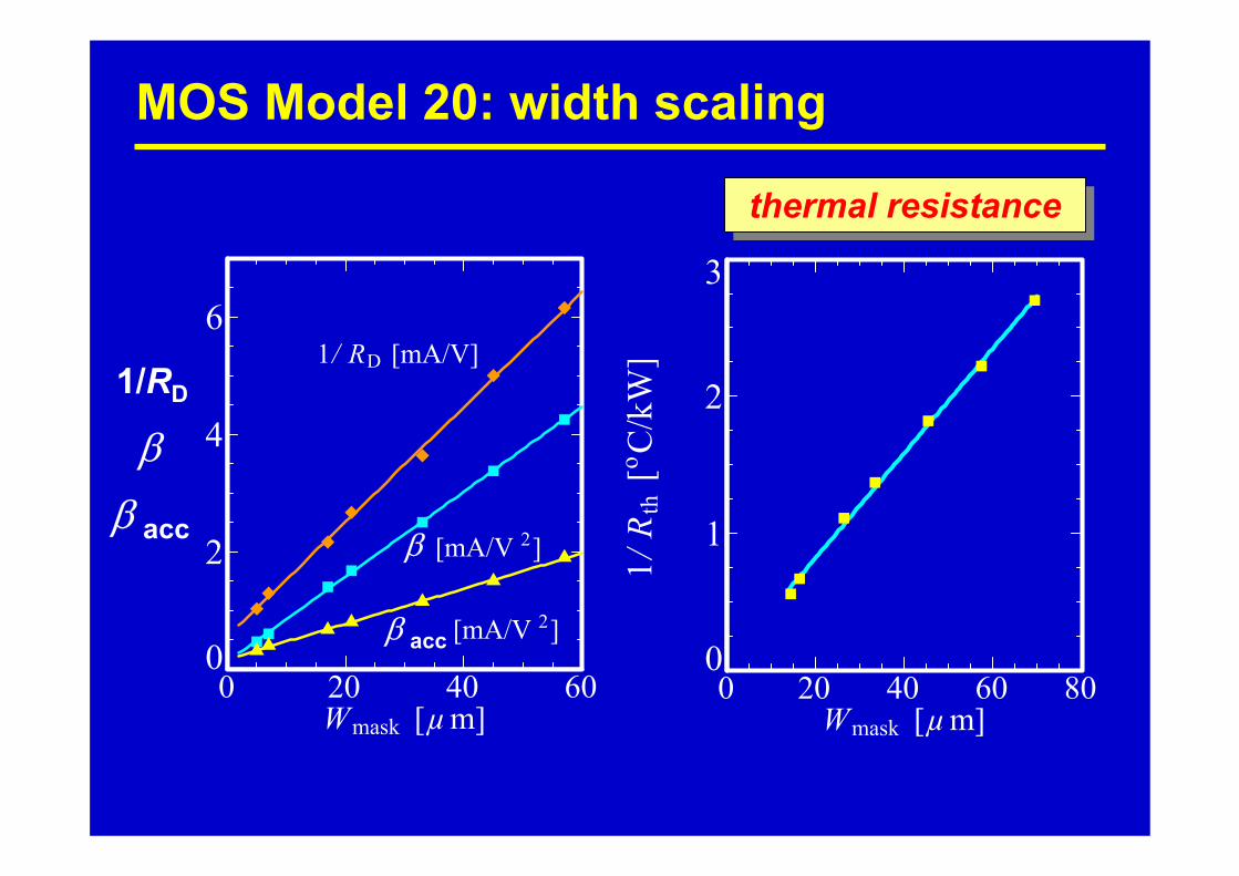
MOS Model 20: width scaling
0 20 40 600
2
4
6
W mask [ µ m]
1 / R D [mA/V]
[mA/V 2 ]
[mA/V 2 ]
β
ββ acc
β acc
1/RD
0 20 40 60 800
1
2
3
W mask [ µ m]
1 / R
th[ o C
/kW
]
thermal resistancethermal resistance

MOS Model 20: width scaling12V SOI-LDMOS: Tox = 38 nm, L = 1.6 µm, T = 25 oC
W = 5 µmIDS[mA]
VGS = 3V
VGS = 6V
VGS = 9V
VGS = 12V
VDS [V]
W = 114 µm
VGS = 3V
VGS = 6V
VGS = 9V
VGS = 12VIDS[mA]
VDS [V]
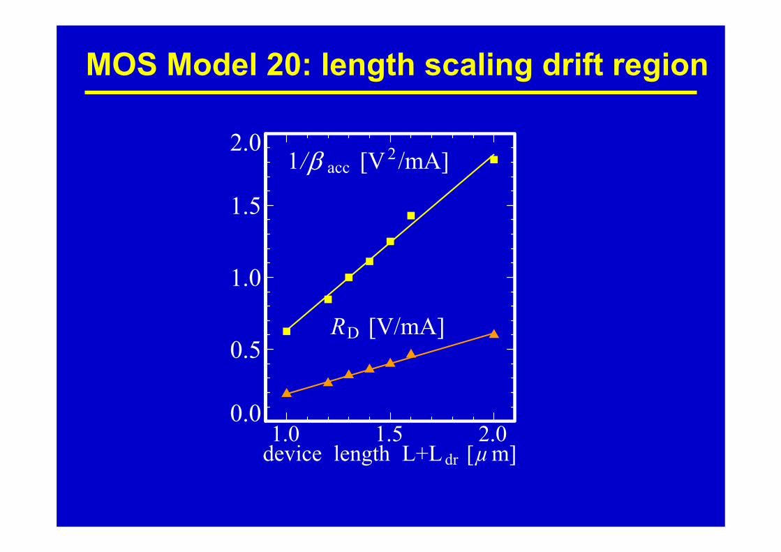
MOS Model 20: length scaling drift region
β
1.0 1.5 2.0 0.0
0.5
1.0
1.5
2.0
device length L+L dr [ µ m]
1 / acc [V2 /mA]
R D [V/mA]

L + Ldr = 1 µm L + Ldr = 2 µm
VGS [V]
I DS
[mA
]
VGS [V]
I DS
[mA
]VSB = 2V
VSB = 1VVSB = 0V
VDS = 0.1V
VSB = 2V
VSB = 1VVSB = 0V
12V SOI-LDMOS: Tox = 38 nm, W = 17 µm, T = 25 oC
MOS Model 20: length scaling drift region
outline
• introduction• MOS Model 20
– basic model– additional model features
• parameters• self-heating and temperature scaling• geometry scaling• bulk current• noise
• summary

VDS =13V
MOS Model 20: bulk current
VGS [V]
I B/ W
[µ
A/µ
m]
VDS =11V

outline
• introduction• MOS Model 20
– basic model– additional model features
• parameters• self-heating and temperature scaling• geometry scaling• bulk current• noise
• summary
MOS Model 20: noise
included: noise from the channel region
• 1/f noise• thermal noise• induced gate noise• correlation
as in MOS Model 11
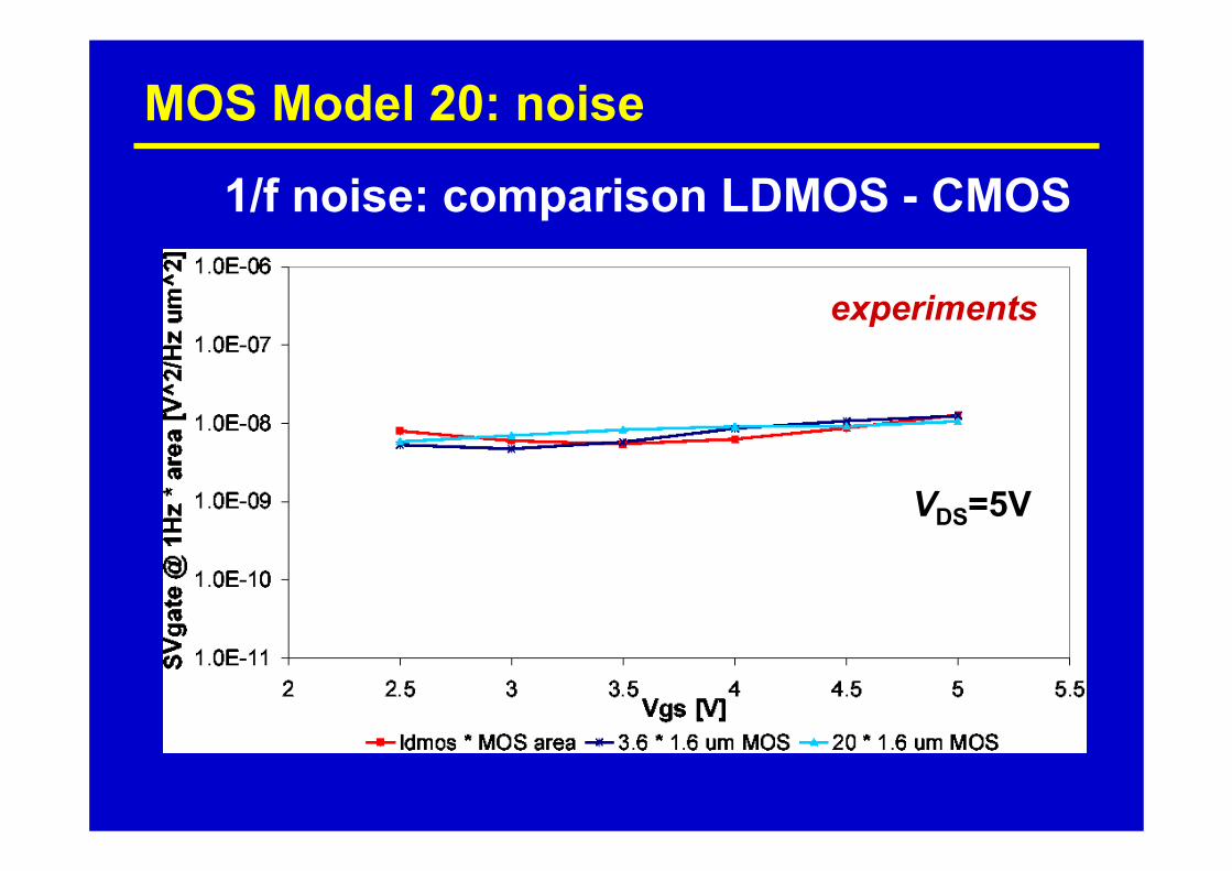
MOS Model 20: noise
1/f noise: comparison LDMOS - CMOS
experiments
VDS=5V

MOS Model 20: noise
1/f noise: dependence on drift region
experiments
VDS=5V

MOS Model 20: noise
included: noise from the channel region
• 1/f noise• thermal noise• induced gate noise• correlation
as in MOS Model 11
supported by experiments
outline
• introduction• MOS Model 20
– basic model– additional model features
• summary– circuit behaviour – “must have” list– concluding remarks
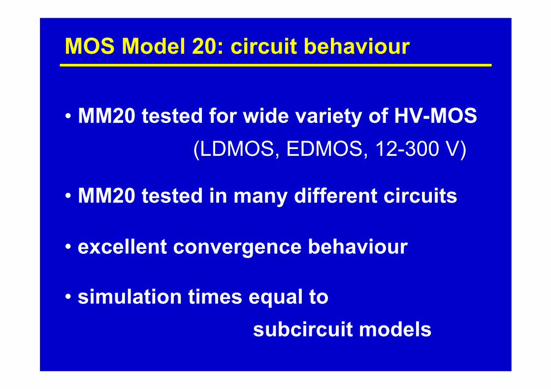
MOS Model 20: circuit behaviour
• MM20 tested for wide variety of HV-MOS (LDMOS, EDMOS, 12-300 V)
• MM20 tested in many different circuits
• excellent convergence behaviour
• simulation times equal to subcircuit models

accurate DC/ACderivatives of terminal currents and node charges charge conservativevoltage-drop across source- and drain
1a
drift region resistance, incl. velocity saturation1b
drift region capacitance1c
parasitic effects1d
1/f, thermal, gate-induced noise1e
OKOK
OKdrain OK
OK
OK
via sub-circuit
OK
MOS Model 20: “must have” list

Vsupply up to 200VT = – 50 till 200 oC
2
self-heating and temperature-dependence parameters3
quasi-saturation, and gm fall-off4
CGD drop5
source-drain resistances, and junctions6
OK, till ~100V
OK
OK
OK
OK
via sub-circuit
OK substrate current7
MOS Model 20: “must have” list

geometry scaling, with one parameter setdrift region length as parameter
8
reverse working (VDS < 0)9
both p-type and n-type10
breakdown behaviour11
good convergence in circuit simulation12
OK
OK
can be added
OK
X
OK
MOS Model 20: “must have” list
outline
• introduction• MOS Model 20
– basic model– additional model features
• summary– circuit behaviour – “must have” list– concluding remarks

MOS Model 20: concluding remarks
• MOS Model 20 gives good description of• currents • capacitances
of LDMOS devices (verified up to 100V)• good convergence behaviour• most items on CMC list included

MOS Model 20: concluding remarks
• on websitehttp://www.semiconductors.philips.com/Philips_Modelsdocumentation and source code available
• C-code• interfaces directly to e.g. Spectre, ADS, …
• supporting institution:• Eindhoven University of Technology• A.C.T. Aarts: [email protected]

• A. Aarts, N. D’Halleweyn, R. v. Langevelde,“A surface-potential-based high-voltage compact LDMOStransistor model”,IEEE Trans. Electron Devices, Vol. 52, No. 5, 2005
• A.C.T. Aarts and W.J. Kloosterman“Compact modeling of high-voltage LDMOS Devices includingquasi-saturation”,IEEE Trans. Electron Devices, Vol. 53, No. 4, 2006
MOS Model 20: literature

TU/e