Embed Size (px)
Citation preview
Y-branch Optical Wavelength
1\1ulti/Demultiplexers
by Ion-exchange in Glass
by
Feng Xiang, M. Sc.
Electrical Engineering Department
McGill University, Montreal
February 1995
A thesis submitted to the Faculty of Graduate Studies and Research in partial
fulfillment of the requirements for the degree of Doctor of Philosophy
@Feng Xiang 1995
.... Nallonal Llbrar;of Canada
SIbllolheque natIonaledu Canada
ACQuISItIons and DirectIon des aCQuISItIons etSIbllographlC ServIceS Sranch des servIces bIblIographIques
J9~ '1b~I:ln'l:on Slrf~:
Ortaw;, On:;lrIO1<1;' ON':
395 rUé WelllnqtonOrt~wa fCM:ano)I<lAON4
',"",' ','r • " ,..1""'\:..
0.;"'''' '\00.••,. .........-...: ..
The author has granted anirrevocable non-exclusive licenceallowing the National Library ofCanada to reproduce, loan,distribute or sell copies ofhisjher thesis by any means andin any form or format, makingthis thesis available to interestedpersons.
The author retains ownership ofthe copyright in hisjher thesis.Neither the thesis nor substantialextracts from it may be printed orotherwise reproduced withouthisjher permission.
L'auteur a accordé une licenceirrévocable et non exclusivepermettant à la Bibliothèquenationale du Canada dereproduire, prêter, distribuer ouvendre des copies de sa thèsede quelque manière et sousquelque forme que ce soit pourmettre des exemplaires de cettethèse à la disposition despersonnes intéressées.
L'auteur conserve la propriété dudroit d'auteur qui protège sathèse. Ni la thèse ni des extraitssubstantiels de celle-ci nedoivent être imprimés ouautrement reproduits sans sonautorisation.
ISBN 0-612-19697-6
Canada
•
•
•
T" Ill" \\"i:·.·. ~lillrt· Cl!.
with lu\·~\ and grar.itl1dt·
•
•
•
Abstract
.\ ~irllplt· ;md ac'tïtra!t' IIllllti:·dll·j'{ I3n'W:'fl'[ angl1' IIW;l:-;lIrt'i!l('Ili t('c1JIliqiH' ha:-
111"'IlI!"\"I'!lljll'd fIl nwa~llrl':--tlh:'trarl'iIldic(·:-;. Bllrh I~- and '\~- iUIl-t'xdtangpd uprical
\';;l\"!':.!.llid ..:-> ill gla~:-; :-;ll!lstratl's \1:1'[(' ('liaractf'rizl'd fur infran'd w;l\"l·Iî'tlgrhs ~\ = 1.152
and 1.j'2:~J1111. For TlH' cl1aractl'rizarillii of :\g- ion-l'xehang(' wavl'g,uidt>. thC' \\l\.B
n"'l hod ha." [,l'.'n lIlodifi"d ro handl" the ind"x truncat ion point at th" waveguide
[,ollll<lar~' insid" the substrat" accuratdy. ..\n explicit and ~tabl" finit,,-difference
\"l'clor I,,'am propagation mt:'thùd has also be"n develop<'d for dfici(,llt num('rica! sim
nlations of th(' gllided-wa\"e optical de\·ices.
:\ 1Il0dified Y-brandi wa\"el('ngth lIIultijdemultipl<,xer (abbr('\'iat<'d as \\"O~l)
for ,\ = 1.31 and 1.55/lm was d~igned and optimized by the beam propagation
mt:'thod (abbre\'iated as BP~I). The de\·ice. made by K'" ion-exchange in glass with
a sputterecl Ah03 strip on one branch. can prv\'ide high extinction ratios and wide
bandwidth. It was sllccessfr;lly fabricated. The me:.;sured results of O\'er 20db extinc
tion ratio agree weil with the BP~1 design simulations. A new Y-branch WO),I made
by K+ and Ag+ ion-exchanges was proposed and fabricated. It eliminates a difficult
fabrication process. in\"ol\"ing an Ah03 strip wa\"eguide. and still pro\'ides the other
merits of the first de\"ice. Its feasibility has been experimentally established. Ta
simplify the fabrication process further, an asymmetric ;\Iach-Zehnder WOM by one
step ion-exchange for bath two-wa\"elength and three-wa\"elength (>. = O.98J.Lm being
the third wa\"elength) was proposed. The BPM simulations show sorne impro\"ements
in se\'cral aspects O\'er other types of demultiplexers.
•
•
•
Résumé
l"w' it'l':l:Üql!\' :--iIllplt'I'! prl'C:.:"· llliii:-:ilZli \!t'~ an~!t':-: i3rt·\\·~t\·r "::l1liti:--i:t't,t" a I~i,~
d,"':f'lUpt"'\' pOUf rneSllrt~r Il'~ indiCt';-' dt':" snhsi:-:li:'. DI':-' .~:lÎ\~I':'" <\!,Iiql:t':-' fahr:qtlt':-; i1;lr
:'0("ilall~t'-i0!W0\' de 1,'- ;,PIlL::--:,i::::l- l.It1 .-\..~ - ',;::"~I'!It \ ILu::-- llll :--Ilh:-,irat li.' \"t'lTt' llllt
lal)(lith"l~ l'nUl" prnpreIlH'Ilt n'thirt' ~'IJIl1ptt) Il' p,)iur rnHlqllt'· dl' Ilildil'(' .\ LI hlllirt' du
guidp il. lïutêriellr du ~ubstrat. Dt' plus. ~ln \'t'r~il1tl explicit,· t'I staill,· dt' la tlIt"rlllldt'
FD-BP:"! ("Finite Difference Bearn Propagation ;'[ethod··) a l't" .'mpl,>yl' pc'ur [e"
simulations efficaces et numériques des guides optiques.
Cn guiJe J'onde du type "Y-branch" (abrégé \\"0:"1) a étl' utilis(' pt modifié
pour réaliser un multi/démultiplexeur pour les longueurs J·olld.,s .\=1.:31 l't Lj5/LIll.
Ll's Illul ti!dl'Illultiplexeurs onr é! é t'on,us et OP! imisés ut ilisanr la ml'! h, >d., Br:..l.
L·appareil. qui a été fabriqué a\'ec succès par l'échaage-ioniqllc K- dans Illl ~ub~tr:l\.
de verre ,wec une bande de .-\\203 (oxide cl'aluminum) po~tilloné(~ ~ur un!' bnulche,
peut donner Jes tau., d'extinctions très hauts et des bandes de fréquences larges. Des
nouve,ms Y-branch \VDM fabriqués par plusieurs échanges-ioniques Je K+ ('t Ag+ ont
été propsés. Le nouvel appareil possède un procéssus de fabrication facile, impliquant
un guide optique de bandes Ah03, et fournit les avantages et mérites de l'appareil
précédant. Sa faisabilité a été établie e.'Cpérimentaiement. Pour simplifier le pro
cessus de fabrication d'avantage, un Mach-Zehnder WDM asymétrique fabriqué par
échange-ionique d'une étape pour deu.'C longueurs d'ondes et trois longueurs d'ondes
('\=O.98~m a été la troisièime longueur d'onde) a été proposé. Les simulations BPM
démontrent des améliorations dans plusieurs aspects par rappart au., autres types des
démultiple.'l:eurs.
• .-\cknowledgements
, '1 .:;;::: ;.~
. . .:::,. ;'1 \'lJ::qlil·r,· rn!;- '::":;':.
•
•
~radllat.· stll<i"llts ur our Glli.il'<i-\ran' Photonil"s Labllr,uory. Dr. K. Kishioka. Dr.
;\, (;,)tu. ~1"'NS L. Babin. D. h:o'n. P. Allarel. J.\". Chen. J. \ïkoloJloulos. ~l.A.
S.'k..rka-Bajbus. and L. Chen for their assistances and encouragement.
Finali,\'. ! "'oulel also likl' to thank ~lr. .Joseph :'!ui. our electronics tecillliciall
This n'sl'arch ,,"as sUJlJlurt<',j by :'\SERC and :'IcGill ulli\'(~rsity through a strate-
;;ic ;;rant. ll[H'ratillg grants. a :'IcGill major fl'llll\\"ship. and a Principa!'s Dissertation
tdlo,,"ship.

•List of Svmbols
~
~\
,"~
1-1.EHn(x.y.z)nu
Pu':0
-'
ka.3n,".
nrkrlItr;;
n,
• nbnex,fAi, BiPo\'b\Vd, Ds(J
D.ERWDMDM
•
\\"ayp!rugt hrime dl'pl'ndt'nt \"('ctdr {lf l'lt'l'ail' iit'ldt itnf' drpl'ndt'llt \'t'ct t)r ()f tlla~ :It't H- til·Id1in\(' indt'I,,'n,!<'nl \"",'l<'r <lf ,'krtrir fit'!drinH' indl'IH'ndl'Ilt n'ctnr nf mag,nt't il' lit'Idrpfract i\"(' ind~xft'frarth"p indpx in rn't' ~paCI\
pt.'nnr·ability of \'aeUU11l
p~rmitti\"ityof vacuumangular frequt'nrywave number in fr~e spart'propagation constanteffective index .3/katransverse wa-"e numberreference refractive indexreference wa\"e numberfield componentfield component after term exp(-jà z) (or exp(-jkrz)) dropp.:od l'rom lItsurface refractive indexsubstrate refracti\"e indexcladding film refracti\"e indextuming point in \VKB methodcladding film thicknessAiry functionsphase integralnormalized freqencynormalized propagation constantwa\"eguide widthwa\"eguide depthswa\"eguide (or branch) separationbranch anglediffusion coefficientextinction ratiowa\"elength di\'ision multi/demultiple.xerdemultiple.xer
•
•
•
\\EH\i\\h!~
1-.1 \ 1
1J- l'FI)FI J-H! '\1FF'J -!~I'\I
'l'He\I-Z
\\',-tlf If'). 1"'::;111:'-[;-" Brill. Illiil. ;l!ld .rt·;rr'·" :::1'! Illl<!
r:l,l/lilit'f: \\"1"':13 ::WrhlJf:
IJ";tnl pr. !p;t;,;:l! il!!) llll'i !!llt!l )lIf'lrt - Fr;tllkf·j
fi ri i t f '-( i i ff. 'ri '!l( 'f'
filliTI'-liiff"[i'Z!I'I' HP:'!fa:-,t FqllrÎI'r rrau:-;f()rm 13P:,\1r raIl:-,pan'u t !J( III ndar~' Cl liid i t iun:.. l(lc!l-Z, 'h Il< lt 'f in! i'rfprUIlH'T t'r
•Contents
1 Introduction 1
1.1
1.2 \\"a\"c!ength Di\"ision :-lllltijDemultiplexing Techniqll'~ .
:2 \Va\"e Theory and Numerical :'\Iethods for Optical \Ya':eguides•1.3
2.1
Original Contributions . . . . . . . . . . . . . . . . . .
General \ \'""c Equations . . . . . . . . . .
·1
10
10
2.1.1
2.1.2
The W;l\"e equ;ltion for a w;l\"cguiùe
The Fresnel \\-d,\"e equatioll
11
12
2.2 The WKB Approximation . . . . 13
2.3 The Dispersion Relation of a Cladded Surface \Ya\"eguide
2.4 A :\lodified \VKB Method for a Truncated Index Profile
15
li
.) _.0 Bearn Propagation Method . 21
•2.5.1
')-')_.0._
Theory and fonnula.
Absorber boundary
i
21
23
•.) ,-~
.)-_.
28
.) -_. ,
.) ~_.u
Etf<ot:tivp Index :-'Iudeling
.-\ppendix . . . . . . . . 37
:2.8.:3 Derivation of E'l. (:2.61) . . ...•:2.8.1
.) ~ 0)_.\,,;.-
:2.8.-1
Deduce Eq.(:2.-l1) from Eq.(:2.-1:2)
The disper:;Ïllll equation (:2.-15) .
\'on :\eumann stability condition
37
38
3D
-la
3 Y-branch Mode Splitter 42
3.1
3.3
Introduction . . . . . .
Branching Waveguides of \\'eak ;l,Iode Coupling
Dependence of Branch Parameters. . . . . . . .
43
47
49
4 Refractive Inde.... Measurements and Waveguide Characterizations 53
Substrate Indices . .
•4.1
4.1.1 Interpolation
53
54
•.,,
,..
:'lea,,;Hrt'lllellt rt',;n1ts and discussinns
71
5 An _-'\.120:1 Strip Loaded Y-branch "-0:\1 for ,\ = 1.55 and 1.311Ln1 by
K--Na- Ion-exchange in Glass 80
•5.1
- .)-J._
lmroduction .
Principle of Operation
80
5.3 BP:'1 Analysis and Design Optimization
5.3.1
5.3.:2
5.3.3
ER dependence on the branch angle.
ER dependence of the effecti\'e index difference
The optirnized design .
S4
86
88
5.4 Fabrication .. 96
•
5.4.1
5.4.2
5.4.3
5.4.4
Initial fabrication process
Measurernent set-up
Prelirninary rneasured results and discussions .
~vIodified fabrication process . . . . . . . . . .
96
105
lai
109

• G A K - and Ag- Ion-exchanged Y-branch \VD:\I
11:2
116
G. i
fi. :-;
fi.1
6.·j
IIltI'lH!llct.iun ..
Ci,iuC't· ur .-\;;:\0: Dil'lrl,,!!
TIlt' Oprillliz..t! D..,;i;;:1 .,!H! rhe BP:\! Simularions
Dt"ojc'(' Fabricar.ion .
:\[e;lsurement Results and Discussions.
116
Ils
1:20
1:2:2
1:26
ï Proposals and Designs: Mach-Zehnder Wavelength DMs 131
•ï.l Introduction . . . . . . . . . . . . . .
:\lach·Zehnder T\,'o-\Y,\\'elength D1\ls
131
133
ï.:2.1
-., .,1._.-
ï.2.3
Principle of operation. . . . .
De\'ices and their performances
Discussions .
133
136
144
ï.3 Three-wavelength Mach-Zehnder DM 145
ï.4 Appendb:: .....
•
ï.3.1
ï.3.2
ï.3.3
ï.4.1
Principle of operation.
BPM simulations
Discussions
Derivation of Eq.(ï.10)
146
148
150
153
153

•
•
•
:5 Conclusions 155

•List of Figures
2.1 .-\ rrfr;H'tiw indcx profilr 1l~(.r) of a slab \\'a\'Cguidc. . . . . . . . . .. 13
2.2 .-\ rcfractÎvc index profile n~(.r) of a slab \\'aveguide with a cladded thin
layer. . . . . . . . . . . . . . . . . . . . . . . . . . . . . . . . . . . .. 15
2.a .\ refractive index profil~ n2(x) of a .-\g~ ion-exchanged siab wa\'eguide
•with an index tmncation at x=d and a tuming point at x,. The dashed
1· . d' h 0 l'me m Icates t e n; me. . . . . . . . . . . . . . . . . . . . . .
2..1 :'\ormalized b-V plots for a strongly asymmetric linear profile.
li
20
.) _.0 Phase shift dependence on the propagation constant. 0, is one half of
the phase shift at x,. . . 20
2.6 Leap-frog ordering of calculation. where the squares indicate the points
having initial input field values. . . . . . . . 29
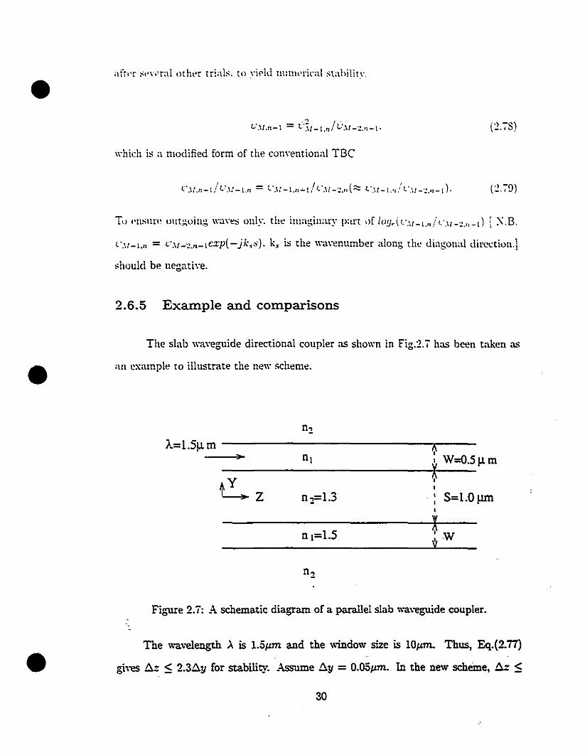
.) _.. A schematic diagrarn of a parallel slab \\'a\'eguide coupler. 30
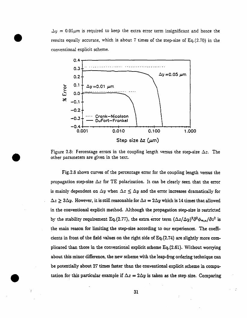
2.8 Percentage errors in the coupling length versus the step-size b.z. The
other paratneters are given in the text. . . . . . . . . . . . . . . 31
2.9 A schematic diagrarn ofthe implementation of the effective index method
for an ion-exchanged channel waveguide. . . . . . . . . . . . . . . .. 34
• 3.1 An asymmetric Y-branch with a small branch angle..
vi
42

• .... .).) •• .J \'"ri"tiùns ùf th~ TE mù,!e patt~rns alùn;\ tht' dir~ctill!l ,)f a hranchin". ~
\\·awguide. a: zero brandI separation: b: small branch St'parati,m: c:
:l.-j
largt' brandI separatiùn. . .
Sc!WIIle of tnode COIl\'l'rsioll in rhl' hranching' \\·a\"('~uidt· ..
·1,
·IS
•
:;.3 Dt'[H'ndclll't' of mod~ amplitudes on tlll' brandI St'parati,m for dint'n'nt
brancL asynlnletries. .. . . . . . . . . . . . . . . . . . . . . . . . .. ,j~l
:3.6 Dept~ndence of mode amplitudes on the brandI separation fùr difft'rent
branch angles. . . . . . . . . . . . . . . . . . . . . . . . . . . . . . .. 51
·t1 Refractive inde:" versus \\<welength, dotted line for BK7 glass and solid
line for soda-lime glass. <5 = 0.0026. . . . . . . . . . . . . . . . . . .. 5-1
-1.2 Reficction from a multi-sheet str:Jcture. nb is the substrate index. lIu
is the index of air, FI and fi are thicknesses of the ith substrate and
air gap, respectively, and m is the number of substrates. 55
-1.3 Reflections of a plane wa\'e near the Brewster angle 'Pb (= 56.529")
from one interface of air-substrate (dotted Hne) and from a substrate
(soHd Hne) with a thickness F = 0.95mm. 56
4.4 ReBections of a plane wave near the Brewster angle 'Pb (= 56.529")
from a multi-sheet structure (solid Hne) \Vith m = 5, Fi and fi (i =
1,2,· . " m) are randomly chosen between (0.945mm, 0.955mm) and
(0.0, 1.0J.Lm) respectively . 5;
•4.5 See the. caption of Fig.4.4 but with m=20. The dashed line indicates
the range of '}! measurement error in 'Pb for one air-substrate interface. 58
•·I.G TIlf' dl'[H'ndl'nrl" of .\1,0, filmrefnwliw indl'x and il' spun"ring; rat('
on t1lf' targ<·t voltag;e at .\ = 0.63:2Spm. . . . . . . . . . . . . . . . .. 63
.1.T Rl'fraC"tiw indl'x \"f'TSllS wavl'Ieng;th. doUt'cl line for tht' hulk of .\1,03
and sol id line for the of ,.1,.1003 spu[[('rl'd at 0.T5 kv Target. volt.age.
~.S
li = 0.1~056 .
The mode indices measurement set-up.
6~
65
•
•
~.9 Theorerical dispersion cu!""es (Gaussian profile) of the guided TE modes
compared with measured mode indices ar .\ = 1.153"m for samples
made ar 385°C. Diffusion times are indicated in minutes. After [il .. 6T
.1.10 Theoretical dispersion curves (Gaussian profile) of the guided Tl\I
modes compared with measured mode indices at .\ =1.153"m for 5an1
pies made at 385°C. Diffusion times are indicated in minutes. After
[i] 6i
4.11 Theoretical dispersion curves (Gaussian profile) ofthe guir.ed TE modes
compared with measured mode indices at >. = 1.523"m for 5an1ples
made at 385°C. Diffusion times are indicated in minutes. After [il .. 68
4.12 Theoretical dispersion curves (Gaussian profile) of the guided TM
modes compared with measured mode indices at >. =1.523"m for sam
pies made at 385°C. Diffusion times are indicated in minutes. After
[i] 68
4.13 The effective guide depth d versus the square root ofthe diffusion time
for the TE modes. After [i] 69
4.14 The effective guide depth d versus the square root of the diffusion time
for the TM modes. After [i] . . . . . . . . . . . . . . . . . . . . . .. 69

• ..L10 .-\ :'\dH'Inatic diagraIll t)f a ~il\'t'r hHl.t'xchaIl~ed planar wan'guîdt' indt'x
profile (",)Iit! line,,) with a ill,kx truncation at x=,l. Th" daslwd lilH'
dpnotcs the \·alue of the (·ffpctin" in<il'x J'Zr. TIH' tllrIliIl~ pnint .ft is gi\'t'Il
by the point of intersection bNween the da.<hed line and lht' s,,!id lillt'.
4.16 The surface index change dep,'ndence on the diffusion time for TE
-.).-
modes at A = 0.6328/,711 at 325"C. . . . . . . . . . . . . . . . . . . .. 7.1
4.17 Theoretical dispersion cur\'cs. - :\1\\'KB and ..... \\'KB. of guided T:\1
modes are compared with measured mode indices at ,\ = 1.152/,71I for
samples made for different time durations (in minute) at 325°C. . .. 75
4.18 Theoretical dispersion cun'es, - M\VKB and ..... \\'KB. of guided
modes are compared with measured mode indices at A = 1.523/,m for
•TE modes for single mode samples at 325°C..
4.19 Sel' the caption of Fig.4.1S but for T:VI modes.
4.20 Index profile depth parameter versus square root of diffusion time at
76
76
,x =O.6328JLm for Tr..<l modes. . . . . . . . . . . . . . . . . . . . . .. 7i
4.21 Inde.'I: profile depth parameter versus square root of diffusion time at
,x =1.152JLm for TE modes. . . . . . . . . . . . . . . . . . . . . . .. 7i
5.1 The configuration of a Y-junction demultiple.'l:er, where ,xl = 1.55JLm,
,x2 = 1.31JLm. 81
- ?'l._ Dispersion curves of TM mode in both branch l and branch 2 when
they are completely separated. The parameters are given in JLm. • .• 82
•5.3 The dependence of ER on the branch angle 8, where 81 = 82 = 8/2,
W I =W2=WO = 4.5JLm, DI = 5.0JLm, O2 = l.OJLm, and f=O.55JLm. .. 85
• 'J.: TIll' d..p..nd ..nc.. of ER. on tlw angle e" \\"here e= a.oo.) rad. e, = e-9" .\\', =\\'"=\\'0 = 4.5Wn . DI = .).Ollm. O2 = l.O/lm. and f=O.55/Lm. .. 86
;, .•J Extillct.ion ratio verslIs the effective index difference bet\\"ef'n t.he t\\"o
Our.pllt. hranches at '\1 = l.551l !Il. The de\'ice parameters are given in
t 1", texl. . . . . . . . . . . . . . . . . . . . . . . . . . . . . . . . . .. 87
:J.G Extinction ratio versus the effectiw index difference het\\'een the t\\·o
"lit pur. branches al. ,\" = l.31ILm. The de\'Ïce parameters are given in
the l.ext . ss
•
.).7 BP:-'I rp$ults (T:\!) at >. = l.55/Lm, ER=32dB and its device 10ss •
O.18dB, for the device with 8 = 0.005 rad, 82 = 0, V..•I=vV2=\Vo=4.5/Lm,
DI = 5.0/Lm, O2 = 1.25/Lm, and f=0.55/Lm. . . . . . . . . . . . . . .. 95
5.8 BP:\! results (TM) at ,\ = l.Sl/Lm, 29dB and its device 1055 -O.lïdB.
for the device with 8 = 0.005 rad, 82 = 0, vVI=W2=VVo=4.5/Lm, 0 1 =
5.0IHI1. O2 = l.25I'm. and f-0.55I'm. . . . . . . . . . . . . . . . . .. 9·5
5.10 The first photo-mask for making the first K+ ion-e.xchange. The other
two de~ices in the mask are not shown. The difference is only in the
w'<lveguide "idth. . . . . . . . . . . . . . . . . . . . . . . . . . . . .. lOS
5.11 The second photo-mask for making the second K+ ion-e.xchange. The
other two devices in the mask are not shown. The difference is only in
the waveguide width. . . . . . . . . . . . . . . . . . . . . . . . . . .. lOS
5.12 The width measurement of an aluminum-mask window by slab diffrac-
tion technique. .......................•...... 104
•
5.9 A flo\\' chart of the initial fabrication process.
5.1S The measurement set-up..
102
106
• ').1~ Output 'pot, at th" "nd faet'! of a O\lmad,' thmu~h lh,' initial fabri
cation l'roc",,'. \\"o=\\"1=5'~JIm. \\"~=5.62Iml. 01=3.711111. 0~=2.511111.
~O·01111 lU7
5.15 Output field amplitudes of '10\·1 madl' through th,' initia! fabrication
prol'ess. . .
5.16 The roughness of ..1,,1"03 strip edges formed by \\",'t-et,hing.
1lJ8
108
5.1'j The third photo-mask for mak' ..g an Al~03 strip \\"id('r than the second-
h:- ion-exchanged branch. . . . . . . . . . . . . . . . . . . . . . . ., 109
5.18 \Iodified fabrication process flo\\" chart. 110
•
•
5.19 Output spots at the end facet for a de\'ice describcd in the text. 114
5.20 Output field amplitudes. . . . . . . . . . . . . . . . . . . . . . . 114
6.1 Configuration of a Y-junction multijdemultiplexer, where branch 1 is
made by h:+ ion-e.xchange and branch 2 by Ag+ ion-exchange. . . .. Il ï
6.2 The sketch of the dispersion curves for both individual branches,D~ is
the upper limit of D2 and Di is the lower limit of D2 for ER > 20 dB
at both wavelengths. . . . . . . . . . . . . . . . . . . . . . . . . . .. 119
6.3 The a110wed fabrication tolerance of D2 versus the surface inde.x change
in the Ag+ ion-e.xchanged waveguide for the ER over 20dB at both
wavelengths, where WI =W2 =5.0JLm, and DI =5.5JLm 120
6.4 Dispersion curves for both individual arms with W I = W2 = 5.0JLm,
DI =5.5JLm, and D2 =1.9JLm. . . . . . . . . . . . . . . . . . . . . .. 121
rj ..' n,·S'Iit' of Br:.! for tllf' T:'! polarization. ER=2S dB at ,\, = 1.55/":11
• and ER=25 dB at ,À., = 1.31wn for Ir, = Ir" = 5.0/"nl. D, = 5.5'Lm.
and D" = 1.!)/"tll. . . . . . . . . . . . . . . . . . . . . . . . . . . . .. 122
f:.S .-\ top vÎC'\\" of a channel w().\"eguide made by :\g- ion·cxchange through
an IIntrpatl'd a!lImitlllnt rnask...
G.;- Th" A.l-ma;;k anodization st't-up.
123
f;.S Fabrication proet'ss for making brandi 2 by Ag~ ion-exehange. 12G
G.!) :\car-field output spotS at the end facet for a K- and Ag-- ion-exchanged
D:'L 11'1 = .5.0 ± O.4iLm, 1F2 = 5.7 ± O.4iLm. Dl = 5.5 ± O.l,:Lm. and
D 2 = 1.9 ± O.15iLm , 127
G.10 :'\ear-field output field amplitudes for a K"" and Ag"" ion-exchanged
D:\L The device parameters are given in Fig.5.9. . . . . . . . . . . .. 127• 7.1 Configuration of a :\lach-Zehnder DM, a: power dh'ider or combiner,
b: taper region, c: two-mode region, and d:mode splitter.. . . . . .. 132
- .)1.- Illustrations of the wave propagation mechanism through the 4-port
hybrid coupler for both the wavelengths. . . . . . . . . . . . 134
7.3 Light power from the wider branch versus light wavelength.. 135
7.4
7.5
BPM simulation for de\;ce 1.
BPM simulation for device 2.
139
139
7.5 Cun'es of e:'i:tinction ratio versus the input wavelength .hl for both
de\;ces. 140
•
• ............... I~O
7'.5 ClIn'cs of extinction ratio "'er:,l1S tiw t'rrOr in Jiffusion titnt' for dt'vi,,'t'
uIle. Thl' dcsigned ion-exchange tirne is 2S-L5 minutes. 1~ l
-'1,.- Cnrws of extinction ratio '"<'rsus th,' ,'rror in diffusion tillll' for <l,'\·k.,
t\\'o. Th" designed ion-exchange tinte is ~31A ntiIll1tl'S. 141
•
ï.1O Curves of extinction ratio \'ersus the error in \\'awguiJe \\'idth for d,!\'iee
one. The \-alue of ~ \\' is assumed to be th,' saille for al! \\':\wguides in
the de\·ice. . . . . . . . . . . . . . . . . . . . . . . . . . . . . . . . .. 1~2
ï .11 Curves of e:'l:tinction ratio \'ersus the eITor in \\'aveguide \\'idth for device
t\\'o. The value of ~\V is assumed to be the same for aU \\'aveguides
in the de\·ice. ..... . . . . . . . . . . . . . . . . . . . . . . . . .. 1~3
ï.12 Cun'cs of extinction ratio versus the change in dilfusion time for deviee
t\\'o, ",hen a \\'idth error has been detecteJ. Cun'es on the left siJe of
the dashed line are for ~\\'=-0.15iLm and those on the right side are
for ~\V=0.15iLm .
ï.13 Configuration for a three-wavelength Mach-Zehnder DM.
ï.14 Illuistrations of the \\'ave propagation mechanism through the 4-port
hybrid coupler in the first interferometer.
143
145
146
ï.15 The device's latera! effective index profile used for BPM simulation. 151
•ï.16 BPM simulation of the whole device for Al = 1.55iL!ll.
ï.1ï BPM simulation of the whole device for A2 = 1.31iLm.
ï.18 BPM simulation of the whole device for A3 = 0.98iLm..
151
152
152
•List of Tables
-1.1 Constants of the dispersion Eq.(-I.l) at 2-1°C .
~leasurement rcsults for BKi glass substrates (m=20) .
5-1
59
-1.3 ~leasurement results for soda-lime glass substratcs (m=26). *: the
value obtained from Eq.(-I.2) . . . . . . . . . . . . . . . . . . . . . .. 60
-1.-1 Indirectly measured Ah03 film index and thickness for O.i5kv target
voltage (P=2i.5w), m is a mode number. . . . . . . . . . . .. ... 62
• -1.5 Constants of the dispersion Eq.(4.5) at 24°C 63
4.6 Measured surface inde."< change ~n, and the effective diffusion con-
stants De at T=385° C. After [il iO
4.ï Comparisons of measured T~I-mode indices with theoretical values for
a sample prepared at T=385"C and t=2130 min. After [il ..... iO
4.8 Measured average surface inde."< changes at 325°C . . . .
4.9 Measured square root of diffusion coefficients (JLm;Jiiilii).
ï4
ï5
•5.1 A chart of ~nel and ~ne2 (xlO-3) distributions versus Dl and f for
D2=1.0JLffi and Wo=4.0JLffi. The parameters, À, Dr, and f, are all in JLffi 90
xiv
- .) .-\ chan of ~nd aad ~n,~ (x lO-3) distribmion,; ,",'r';llS 0: and l' f"r:).-• D~=l.Ollm and \\·u=·L5pm. The parametl'rs. ,\. 0:. and f. are aIl in lall 911
5.3 A chan of ~nd and ~n,~ (x 10-3) distribution,; \','r';llS Dl and f ftlr
D~= 1.0llm and \Yo=5.0ILm. The parametl'rs. ,\. 0:. and f. art' aIl in l'Ill 91
G.~ .-\ chan of ~Tld and ~n,~ (x lO-l) .iisrrihuti.,n,; \'t'r';ll'; D, and f f"r
D~=1.5Ilm and \Yo=~.OplII. The parallll'tl'rs. ,\. Dl, and f. are aIl in Iml 91
5.5 A chan of ~nd and ~n,~ (x 10-3) distributions \'ersllS D, and f for
D~= 1.51Lm and \\·o=L5Ilm. The parameters. ,\. Dl, and f. art' aIl in /llll 92
5.6 A chan of ~nd and ~n.2 (x 10-3) distributions wrsus Dl and f for
D2=1.51lm and Wo=5.0Ilm. The parameters. ,\. Dl, and f. are ail in ILm 9:!
5.7 A chart of .6.nd and ~n.2 (x 10-3) distributions \'ersus Dl and f for
D2=2.0Ilm and Wo=4.0jlm. The parameters, ,\, Dio and f, are ail in jlm 93• A chan of .6.nd and ~n.2 (x 10-3) distributions \'ersus Dl and f for5.8
D2=2.0jlm and \Vo=4.5Ilm. The parameters, À, Dt. and f, are ail in l'm 93
5.9 A chan of ~nd and .6.n.2 (x 10-3) distributions versus Dl and f for
D2=2.0jlm and Wo=5.0jlm. The parameters, À, Dl, and f, are ail in l'm 94
5.10 Extinction ratios for a device with ~Vo = Hrl = 5.32 ± O.4l'm, W2 =
5.02±0.4l'm, Dl = 5.0±0.ljlm, D2 = 1.5±0.1I'm, and f = 0.56±0.02I'm.112
7.1 Extinction ratios 150
•
•
•
•
Chapter 1
Introduction
1.1 Historical Overview
In the early 1980's, the progress of single-mode optical libers made a signilicant
impact on light\\"a\'e communication systems due to their lower loss and dispersion
than mlliti-mode libers. There are t\\'o low loss wa\'elengrh windows of a glass liber
arollnd ,\ =1.31Jlm and 1.55Jlm [1], Before dispersion-shifted and dispersion-flattened
fibers were de\'eloped in the middle of 1980's, most optical communication systems
were designed for operation at À = 1.31Jlm window to take advantage of the zero
dispersion of the standard step-inde.\: single-mode libers at À = 1.3Jlm [2], It was
found out lately that the zero dispersion can be shifted to À = 1.55Jlm [3] if the
core inde.'\. profile of a single-mode liber is properl~' designed, Further, with the
development of dispersion-Battened single-mode libers [4] the near-zero dispersion
region covers both the low 1055 wavelength windows, which then pennits the use
of the wavelength-divisi.on multiple.\:ing (vVDM) technique for these two windows to
effect wide band optica1 liber communication systems,
Based on thin film technologies, integrated optics has been an active and rapidly
progressing area of research since 1969 [5], Like integrated electronics, integrated op
tics promises to pro\"Ïde miniaturized and interconnected signal-processing opticai.
1
••
•
•
different kind of ~ub~trate derermin.,~ tilt' ditf.'rpnt t"l'hnl,lo"i,,:, u~,'d in int""rat,'d. .optics (which can al~o be called "Guided-\\'aw Photonil'~". u~inF. th,' l'llrrt'nt t"r.
minology). One of ~uch t..chnologie~ i~ ba.'<'d on th., ll~t' of gla-"~ a.' th,' ~llh>tratt'
mau'rial. The importance of the gla~~ b~l'd l'omponpnt~ i~ bortlP out hy th"ir l'OlU-
patibility with optical fibers. potentia1ly low co~t. low propagation 10~~l':'. and tilt'
case of their integration into an optical fib..r l'ommunication ~y~tPm or ~.'nsor [61 i7j.
Ion-exchange technique. which has been used for mor.' than a l'entury to pro-
duce tinted gla.«s. has recei\'ed increa.'ed attention in recent years as it improvcs
surface-mechanical properties of gl~ and. more importantly. creatcs a wavt'guiding
region in the glass. Since 19ï2 when Izawa and :\akagome [8] report.'<! th., fi~t ion
exchanged waveguides by exchange of TI- ions in a silicate glass containing oxides
of sodium and potassium. significant progress has been made towards understanding
the ion-e.'l:change process and the l'ole ofthe processing conditions on the propagation
characteristics of the resulting waveguides. Varions cation pairs and se\-eral different
glass compositions and cation sources have been studied in the past two decades.
Among them Ag+-Na+ [9] [10] and K+-Na+ [11] are considered to be prime candi
dates for making glass Ylaveguides and devices. Findakly [12] and Ramaswamy [13]
summarized most of the developments which occurred until 1983 and 1988 respec
th-ely. After the glass waveguide fabrication techniques (ion-beam rnilling, sputtering
[14], photolithography, etc., besides the ion-exchange) become mature, many useful
glass waveguide devices were proposed, designed, and implemented. Among them,
the wavelength dhision multiple.'I: (WDM) devices made on a glass substrate have
been receiving considerable attention and much progress has been made.
2
• 1.2 Wavelength Division MultijDemultiplexingTechnique
ln princip!e, optical wave!ength multiplexing is quite similar to electrica! mul-
•
•
riplexin;!" Hùwewr. much higher frequencies are employed in optical mllitiplexing,
\\"a\'l'll'ngth di\'ision multi/dernultiplexing (\-VD:-!) a110ws a fiber optica! communica-
rion system to greatly enhance its channel capacity, by using se\'eral working wave-
lengr hs, each capable of carrying multiple channels, It increases the system capacity
withollt mllch increase in cost [15], The important performance figures of a \-VDM
are extinction ratios (ER) which are the ratios between the power from a designed
",a\'eguide to the power leaked illto the other waveguides, power loss, and channel sep-
aration, Severa! kinds of WDM devices have been proposed for different applications,
Optical interference filters [16] pro,,;de high e:"tinction ratios, low loss, and medium
channel separation (30-100nm), Optical diffraction gratings [17] have high extinction
ratios and sma11 channel separation (l-40nm). Wavelengrh selective directiona! cou-
pIers [18] [19] [20] have low loss and large channel separation (40-200nm). X-branch
two-mode interference WDMs [21] and [22] have high e.'i:tinction ratios, large channel
separation (40-200nm), and low loss. Asymmetric Y-branches which ,vil! be the main
topic of this thesis promise to have high e.'i:tinction ratios, large channel separation
(>lOOnm), 10\V loss, and short in length. The asymmetric Y-branch WDM made by
K+-ion e.'i:change with one branch cladded by an Ah03 strip \Vas first proposed by
Goto and Yip in [23] for À = 1.31~m and À = 1.55~m. The measured e.'i:tinction
ratios of the first few fabricated devices were about 10db, far below the theoretical
predictions.
The Y-branch is a very important structure in integrated optics.--It can be either
a power divider or a mode splitter depending on the branch angle and the branch
asymmetry [24]. A wave1ength multijdemultiple.'Cer. made by a Y-branch functions
3
•
•
•
as a mode splitter. On the other hand. for a mode splitter to work as a wavelength
multi/demultiplexer. not only the large branch asymmetry and small branch anglc
but also the branch waveguidc mode dispersion and the waveguidc material dispersion
are the important facts that affect thc de\'ice quality. To improve the initial dcsign.
a detailed study of this new kind of device is necessary. which has not bcen done. or
at least has not been reported. according to our knowledge. From the basic device
concept, the initial goal of this work is to modify the initial design, optimize, and
fabricate the device.
Since the demultiplexers to be discussed in this work can intrinsically work also
as multiple.xers after the input and output of each individual are simply exchanged
and the demultiple.xing with high e.xtinction ratios is more difficult to achieve, we will
drop "multi" from '1nutli/demultiple.xer" and keep "demultiple.xer" (DM) later on to
emphasize our efforts in the optimum design and implementation of demultiplexers.
1.3 Original Contributions
The contributions of this work can be summarized as folloVl"S:
• characterizations of K+ and Ag+ ion-exchanged waveguides at infrared wave
lengths [25] [26]
• development of a simple and accurate substrate index measurement method [27]
• modification in the WKB method for handling a waveguide index profile with
truncation or discontinuities more accurately [28]
• development of an explicit and stable FD-BPM [29]
• modifications in the asymmetric Y-branch WDM with an Al20 a strip load and
also in its fabrication'1?rocess which leads to much improved measured extinction
4
•
•
•
ratios [30] [31]
• proposaI and fabrication of a ncw asymmctric Y-branch WD~I made by a two
step (K" and Ag--) ion-exchange in glass for), = 1.31Jlm and), = 1.55Jlm which
offers an alternative fabrication process [32] [33]
• proposai and dt-sign of a two-wavelength WDM by cascading an asymmet.ric
Y-branch with a Mach-Zehnder interferometer which requires only one-step ion
exchange and yet provides high e.xtinction ratios [34]
• proposaI and design of a three-wavelength (0.98, 1.31, 1.55 Jl m) \VDM by
cascading two of the above proposed two-wavelength demultiplexers [35J.
5
•
•
•
Bibliography
[1] S.S. \Valker, "Rapid modeling and estimation of total spectral loss in optica!
fibers", .1. Lightwa\'e Technol. \'01. LT-4. p.1l26. 1986.
[2] F .P. Kapron and T.C. Oison, "Accurate specification of single-mode dispersion
measurements", Tech. Digist, Symp. Opt. Fiber Measurements, NBC Special
Publication 683 (Boulder, CO, October 1984), p.ll1.
[3] L.G. Cohen, C. Lin, and \V.G. French, "Tailoring zero chromatic dispersion into
the 1.5-1.6 J.Lm low-Ioss spectral region of single-mode fibers" , Electron. Lett., \'01.
15, pp.334-335, 1979.
[4] L.G. Cohen, W.L. Mammel, and S.J. Jang, "Low-Ioss quadruple-dad singl~"'mode
lightguides with dispersion below 2ps/km-nm over the 1.2SJLm-1.65J.Lm wave
length range", Electron. Lett., vol. lS, pp.l023-1024, 1982.
[5] S.E. Miller, "Integrated Optics: an introduction", Bell Sys. Tech. Joum., 48,
pp.2059-2069, 1969.
[6] W.J. Tomlinson and C.A. Brackett, "Telecommunication applications of inte
grated optics and optoe~ectronics", Proc. IEEE, vol. 75, pp15 12-1523, 1987.
[7] S.R. Forrest, "Optoelectronic integrated circuits", Proc. IEEE, vol.75, pp.122
125, 1987.
6
=
•
•
•
[S) T. Izawa and H. :\akagome. "Optical waveguide formed by electrically inàuced
migration of ions in glass plates". App. Phys. Lett.. vol.21. p.SS4. 19ï2.
[9] G. Stewart, C.A. :-'Iillar. P.J.R. Laybourn. C.D.\\". \\ïlkinson, and R.:-'1. De
larue. "Planar optical waveguides formed by silver-ion migration in glass" . IEEE
.1. of Quantum Electron., vol. QE-13, :\0.4, pp.192-200, 19ïï.
[10] G. Stewart and P.J.R. Laybourn, "Fabrication of ion-exchanged optical w:l';eg
uides from dilute sil ver nitrate melts", IEEE J. of Quantum Electron.. \'01. QE-14,
;-';0.12, pp.93D-934, 19ï8.
[llJ G.L. Yip and J. Albert, "Characterization of planar optical waveguides by K+-ion
exchange in glass", Optics Lett., vol.10, No.3, pp.151-153, 1985.
[12] T. Finkadly, "Glass waveguides by ion e.xchange: a review", Opt. Eng., vo1.24,
pp.244-250, 1985.
[13J R.V. Rarnaswamy and R. Srivastava,"Ion-e.xchanged glass waveguides: a review",
IEEE J of Lightwave Tech., vol. 6, No.6, pp.984-1001, 1988.
[14] H. Nishihara, M. Haruna, and T. Suhara, "Optical integrated circuits", New York,
McGraw Hill, 1989.
[15] O.E. Delange, "Wideband optical communication S)'Sterns: part 2-frequency di
vision multiplexing", Proc. IEEE, vo1.58, pp.1683-1690, 1970.
[16] H. Nishihara, M. Haruna, and T. Suhara, "Optical integrated circuits", New York,
McGraw Hill, pp.265-273, 1989.
[1 i] T. Suhara and H. Nishihara, "IntefTated optics components and devices using
periodic structures", IEEE J. of Quantum Electron., vo1.22, pp.847-865, 1986.
[18] M. Digonnet and H.J. Shaw,"Wavelength multiple.xing in single-mode fiber cou
piers", Appl. Opt., vo1.22, pp.484-491, 1983.
7
•
•
•
)9] R.C. A.lfert!ess and R.\·. Schmidt. "Tunabl" llprical \\'a\"t'~ui(ll' din'crillllall"lluph-r
fiird' . Appl. Phys. Lett.. \"01.33. pp.161-163. 1978.
[:2(\] H.C. Ch"n~ and R.\". Ramaswamy. ".-\. dual wa\"elcng;th L;>-lo33)Lm din'crillnal
coupler wawlength t!h'isilln multi- denmltipll·xcr··. IEEE .J. of Lig;htwa\"l' Tl'ch.,
\"01. 7 pp.766-776. 1989.
::21] y Chung..J.Y. Yi. S.H. Kim. and S.S. Choi. "Analysis ùf a tllnahlt· mlllt.ich;ulIld
two mode inrerference waveleng;th di\'ision llIultiplexcr-dcmultiplexer", IEEE .J.
of Lightwm'e Tech.. pp.i66-7i6. \"01. LT-i, 1989.
[:2:2] L. J. ~L Babin and G.L. Yip, "Design and realization of a widened X-branch
demultiplexer at 1.31 and 1.55flm by K+- Na+ ion exchange in a glass substrate",
IPR technical digest vo1.3. pp.• 1994.
[:23] N. GOLO and G.L. Yip, '''Y-branch wm'elength multi- demultiplexer for ,\ =
lo30)lIll and ,\ = 1.5.5flm", Electronics Lett., \'01.:26. pp.10:2-103, 1990.
[:24] W. K. Burns and A. F. ;,\liIton."Mode conversion in planar dielectric separating
\\,t\'eg;uides", IEEE J. QUil.lItum Electon., vol. QE-11. pp.3:2-39, 19i5.
[25] G.L. Yip, K. Kishioka, F. Xiang, and J.Y. Chen, "Characterization of planar
optical waveguides by K+-ion exchange in glass at 1.152 il.lItl 1.523flm", SPIE
conference proceedings, \'01.l583 pp.I4-18, 1991.
[26] F. Xiang, K.H. Chen, and G.L. Yip, "The application of an improved WKB
method to the characterization of diluted silver ion-e.'l:changed glass waveguides
in the near infrared", SPIE conference proceedings, vo1.l794, pp.40-47, 1992.
[27] F. Xiang and G.L. Yip, "Simple technique for determining substrate indices of
isotropie materials by a multisheet Brewster angle measurement", Applied Op
tics, \'01. 31, No. 36, pp.7570-7574, December 1992.
8
•
•
•
2~' F. Xi,,"~ "Ild G.L. \ïp. ".-\ Illudifi"d \\'KB mPf.hor! for t.hl' impro\'"d ph,,,,,, shift.
al. a t.1Irllill~ point". IEEE .Journal of Lighr.w<lw Technology. \'01. 1:2. pp.~-l:l--I5:2.
:>'farch. I!J!J-l.
'2!Ji F. Xian~ and G.L. Yip. ".-\n Explicit. alld st.able finite difîerencc 2-D be;uIl propa-
~at.iun llll't.hod". IEE:E PhUTOIl. TedlIlol. LerL. \·0l.6. :\,>.10. 1'1'.12-18-1:200. 199-1.
':1lI~ F. Xiallg. G.L. \ïp. allr! :\. Gorn. "The analysis alld r!esigll UprilIlizarioll of <l. ,
Y-hranch \\'a\'elcllgth IlltIlri/r!ellllllrip1<'xer for ,\ = 1.:31 alld 1.001/111 by BP:>"".
looe ('ollf,~rellce proc'·"r!illgs. paper Tll.PS1.G. 1991.
[:31] F. Xiang and G.L. Yip. "An Al20 3 strip loaded Y-brancll wa"elength multi/
demultiplexer for ,\ = 1.55 and 1.31JLm by K+-Xa+ ion-excllange in glass". IPR
technical digest, "01.3. 1'1'.130-132, 1994.
[3:2] F. Xiang and G.L. \ïp...:\C\\· Y-brandi \\',\\'elcngth multijdemllltiplexer by K+
alld Ag+ ion exchange for ,\ = 1.31 and 1.5.jJl111" • Electron. Lett .. vol. :28. :Xo.
:24, pp.:2:26:2-:2:263, l'O\·. 199:2.
[33] F. Xiang and G.L. Yip, "A Y-brancll wavelength multi/demultiple.."er by K+ and
Ag+ ion-e.."cllange for>' = 1.31 and 1.55JLm -de\'ice fabrication and measurement
results", GRIN conference proceedings, pp., 1994,
[3-1] F. Xiang and G.L. Yip, "Asymmetric Macll-Zehnder type wavelength demulti
ple.'l:ers" , GRIN'93 conference proceedings, Paper C4, 1993.
[35] F. Xiang and G.L. Yip, "Three-Wavelength Macll-Zehnder demultiplexer" , SPIE
conference proceedings, 1994.
9
•
•
Chapter 2
Wave Theory and NumericalMethods for Optical Waveguides
The theory of guided-wave optics is based on the Ma.xwelI's equations. Waveg
uides and devices made by ion-exchange in a glass substrate are mostly weakly guiding
(1). Sorne approximations can be applied which simplify the wave equations. In this
Chapter, sorne powerful numerical methocls will be presl!nted to solve the wave equa
tion, especially, the beam propagation method (abbreviated as BPM later) and the
finite-difference beam propagation method (abbreviated as FD-BPM later). AlI the
de\·ice designs and optimizations in this thesis work are mainly based on the methods
and schemes presented here.
2.1 General Wave Equations
Ma.xwelI's equations for source free, time dependent fields are
ô'H. (2.1)"V xE = -JJ.o-8t
2 ôE (2.2)"V x1l = n eo 8t
"V·{n2eoE) = 0 (2.3)
• "V.1l = 0 (2.4)
10
• will'n' E and 11. aI'P t,Ill' r.iIlH' di'p"!l<lt'I1t \"('cotors (Jf l'lt'crric and rnagnetÎc fil'ld~ and
"(X.v.z) is 1.111' lIlf·di"l:l refranin' indl'x. Rl'presl'''l.ing btH.h the field wctors in i =
E,·;r.piJ",·t) and 1i. = HCIp(j;.:t). the wctm wave eqllations car. be written as
., .E· \;'J/2(I.!J':)j .,., ~'ii'- E + 'V[ ." _) . + kii Tl" (J:. !J. :).:. = ()n-"' .... !J._
and.) ., )
" 'ii'-II"(,I.'. IJ. : ., .,'ii'- H +,. " x (v x H) + kü,,-(.r.!J. :)H = 0
TI-I,.f. y.':,
(:2.3)
..) 6)\_.
,.
fur !Joch the electric field E and magller:c field H. respectively. \\'here ko = :'-'Vl1o=o the
l'rel' space wll\·enumber. If the l'l'l'l'active index n(x,y.z) varies piecewise slowly with
x. y, and z, the second terms in both Eqs.(2.5) and (:2.6) can be neglected yielding
the Helmholtz scalar wave equation
( 'l -)_..where \1' can be any of the six field components. The reslllting fields will satist~· the
boulldary conditions for any index discontinuity.
2.1.1 The wave equation for a waveguide
For a waveguide, the inde.'i: n is uniform along z and the travelling wa\'e term
e.'i:p(-j,Bz) is understood and can be dropped from the fields. The wave equation (2.ï)
can be reduced
(2.8)
•
where 'i7 .L = éP/8:r? + éP/8y2.
Consider a slab waveguide and assume that its inde.'i: profile only varies in the
x direction (8/8y =0). We can classify into two kinds of mode solutions. One is the
TE modewith
(2.9)
11
• H .il' = --EI/.
•••:J..1n .
H. = _-..L DE"- -'/lo à:r
auel the ,n.her i~ the T:-I IllOt.l~ with
E" = H, = H, = (J.
E'l.(:2.S) is UO\\· ~implified illto
a!t.:~ .) <) "
- -'- [ken-lx) - B-lli! - 0Dx2 ' 0 . - •
(:!.llJ)
(:!.ll)
(:!.1:!1
(:!.1:J)
(:!.l~)
(2.15)
•.-\.~ ~howu in Eq~.(2.9-2.1.j), ail the field components cau he expres~ed by Eu for TE
mode~ and by Hu for T:\I modes. Therefore. only one field component needs to be
~ol\"Cd iu Eq.(2.15). It is assullled in Eq.(2.15) that ~, = Eu for TE modes or l: = H"
for T:\I modes.
2.1.2 The Fresnel wave equation
In most of guided-w,\\'e optical devices, the refractive index profiles of the
waveguides are dependent on z. Here, we assume that the inde., n(y,z) be independent
of x and slowly varies with y and z. This situation would correspond to the region
inside a slab waveguide, infinite along the x-direction but bound along the y-direction
(e.g. y =±a, a being a constant). Ifwe e.'press the field component Ilt in Eq.(2.i) as
Ilt(y, =) = t/J(y, z)exp(-jkonrz), (2.16)
(2.li)•where nr is a reference refractive inde." substitution of Eq.(2.16) into Eq.(2.i) and
use of 8/8x = 0 lead to the following equation for the comple."< field amplitude
fPt/J ? . 8tb fPt/J 2 2 2)8z2 - -1konr 8z + 8y2 + kô(n - nr t/J =o.
12
(2.18)'.
•
:-':e~I('cting the !irst term in Eq.(2.1 i) gives the para'dal or Fresnel wave equation
al" â2 l.J.) 'k ' . k2 ( 2 2). 0- -] on'-a .,.. -a,"" 0 n - n, J.; = .= y-
Eq.(2.18) will be uscd in the beam propagation method (BP:-'I) simulations of waveg
uide devices, employing the effective index method (EI~I).
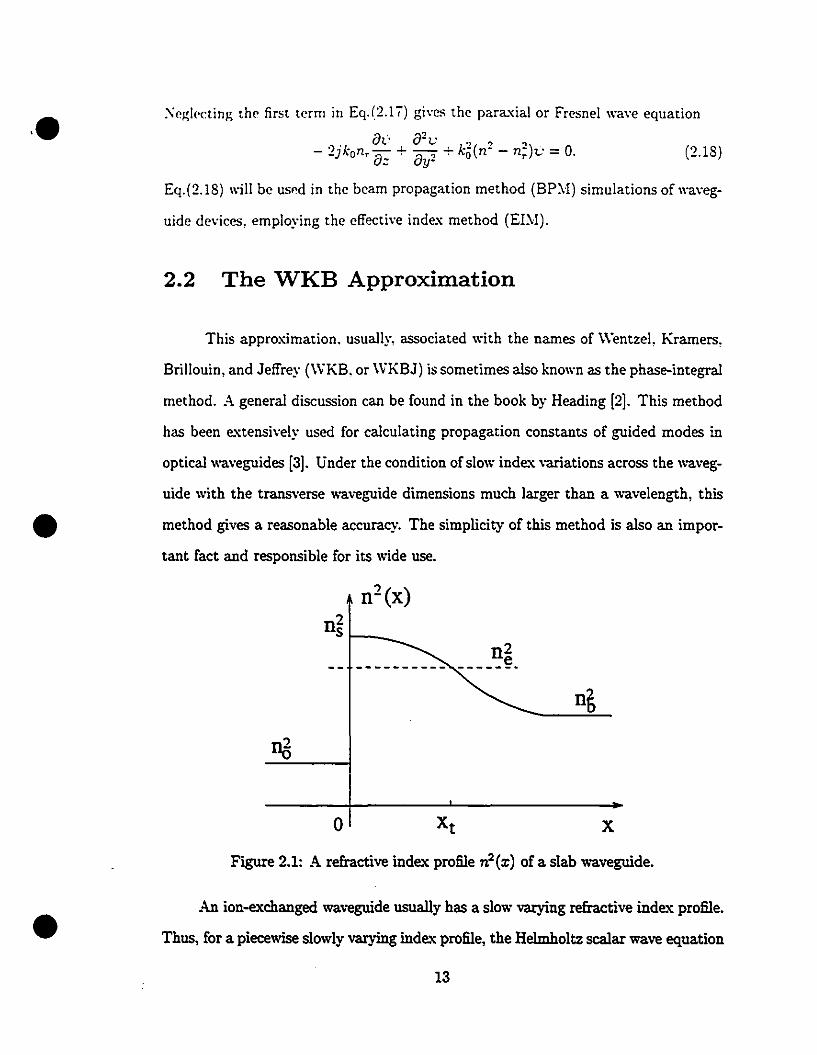
2.2 The WKB Approximation
This approximation. usually, associated with the names of Wentzel, Kramers,
Brillouin, and Jeffrey (\VKB. or WKBJ) is sometimes also known as the phase-integral
method. A general discussion can be found in the book by Heading [2J. This method
has been e.'\(tensively used for calculating propagation constants of guided modes in
optical waveguides [3]. Under the condition of slow inde.'\( variations across the waveg
uide \Vith the transverse .....aveguide dimensions much larger than a wavelength, this
method gives a reasonable accuracy. The simplicity of this method is also an impor
tant fact and responsible for its ....;de use.
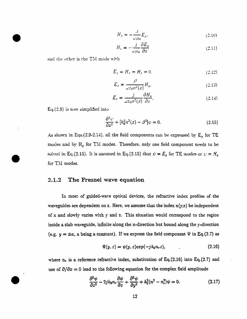
n~ t'"-__
n2-----~.
o x
•Figure 2.1: A refraetive index profile n2(x) of a slab waveguide.
An ion-exchanged waveguide usually has a slow varying refractive inde.'C profile.
Thus, for a piecewise slowly varying index profile, the Helmholtz scalar wave equation
13

•For an index profile snch as rhar. of a surfac(' slab \\"<1\"pguidl' as sho\\"11 in Fi~.~. 1.
rh.· \\"KB field solut.ions are gi\,('n by [-1]
t.' = .-l. ".rpt.r);uPu-) (.1' < 0)
B'"(. == -=co.'ij' QdJ: - :;-/-11v'Cd . ~ .
B . 1~ç == ",,~.l'p - Pt/J:l
2vP . <, •
\\"here A and B are both constants.
(1) <.1' < .r,)
l~·E))
(2.20 )
(~.21)
is kno\\"n as the effective index. and x, is the turning point. At x = 3',. the Airy
funerions. Ai and Bi, solution of the scalar w,we equation for a linear index profile•n. = .:J/ko
(2.22)
(2"~3)
[3]. connect the fields gi\'en by Eq.(2.20) and Eq.(2.21) [-1]. Matching the fields and
their derh"ati\'es at x=O leads 1.0
n= fQdx.The eigenvalue (or dispersion) equation for a surface \\"a\"eguide is then given by
•
B.-l. = J(Jcos[n - 11'/4],
1)t.4.koPo- = BjQsin[n -11'/4],
where
and
(2.24)
(2.25)
(2.26)
(2.28)
14
•
•
•
w,,,,rf' Eq.(2.22) has bpf'n applipd for Po- and Qo-. and the differentiation was not
appii('d to Q in the denominator of Eq.(2.20) because 1/.,jQ is approximately constant
ll<'ar x=O. Eq.(2.28) is the same as that obtained by a rigorous applir.ation of the
gpumetrical opties [5]. It will be used very frequently later on for K- ion-exchange
surface waveguides.
2.3 The Dispersion Relation of a Cladded SurfaceWaveguide
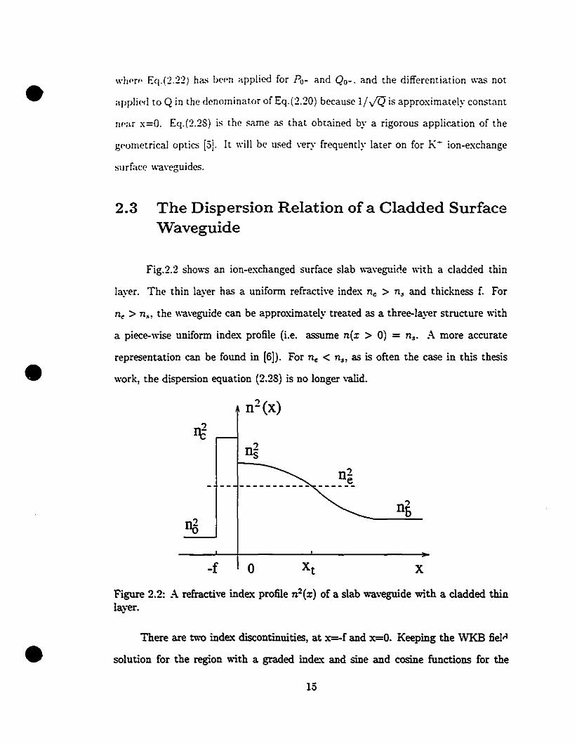
Fig.2.2 shows an ion-exchanged surface slab waveguirle with a cladded thin
layer. The thin layer has a uniform refractive index ne > n, and thickness f. For
ne > n" the waveguide can be approximately treated as a three-layer structure \\;th
a piece-wise uniform inde."\; profile (i.e. assume n(x > 0) = n.. A more accurate
representation can be found in [6]). For ne < n., as is often the case in this thesis
work, the dispersion equation (2.28) is no longer valid.
n2 (x)
nJn2
s
n2e------
n6nô
-f 0 X t X
Figure 2.2: A refractive index profile n2(x) of a slab waveguide with a cladded thialayer.
There are two inde."\; discontinuities, at x=-f and =0. Keeping the WKB fieltl
solution for the region with a graded inde."\; and sine and cosine functions for the
15
• Il\"
," ;\~ .......... - J
1. =
v ==
1.==
B .,fIIlQ,·.ri - LCC).'\Q, .r\ i - / <:. ...: ln
B (.(),:}"" (l,:.. _. "-=" .... -.,.'" )Il...:.: <.,..~v'(2 ',' "
B . ," .'-=! .:"n l - 1 Pli..··' i " ....... " 1\" " ., 1'2\'p "., '
\~ .ill
tan(n - 7:' /-1) = 'Il (J•. S.Qo- C
L'sing the boundary conditions at x=·f. we have
('2.33)
•koJn; - nij BcosQcf -;- C.,inQcf
r~2 =. .Qe CcosQcf - S"I1lQ,.J
{1 for TE maties
'1~ = n~/ ng for T~I modes.
('2.3-1)
(.) 3-)_..)
Soh'ing the ratio (B/C) l'rom Eq.('2.3-1) and substituting it illto Eq.(2.33) yidd the
dispersion relation for the wa\'eguide as
tan(n - ,,/-1) = 1]1 (2.36)
where~ ~
di = tan- 1[..... n;; -Tlii]c .,~.,., •në -n;;
(2.3ï)
•
die is known as the hall' phase shift on the interface of air and cladding layer and
n is given by Eq.(2.2ï). As \\'e can see in Eq.(2.36), the dispersion relation can be
simplilied into a '\-"KB eigen\-alue equation if ne = no.(= n.) .
16
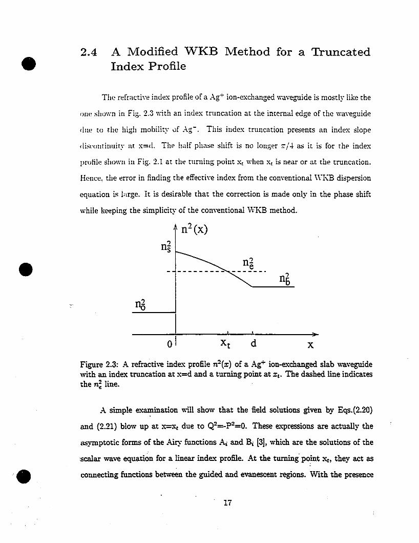
• 2.4 A Modified WKB Method for a TruncatedIndex Profile
The refractive index profile of a Ag-;- ion-exchanged waveguide is mostly like the
•
one shown in Fig. 2.3 "'ith an index truncation at the internai edge of the ,vaveguide
due tel r.he high mobility 0f .\g-. This index tmncation presents an index slope
disl'ourinuiry ar x='\. The half phase shift is no longer -;:/-1. as it is for rhp index
protile shown in Fig. 2.1 at the tllrniug point x, when Xt is near or at the truucatiou.
Hence. the error in finding the effectÎ\'e index from the conventional WKB dispersion
equation is large. It is desirable that the correction is made only in the phase shift
while keeping the simplicity of the conventional "YKB method.
n2e
0 1 d x
Figure 2.3: A refractive inde.'i: profile n2 (x) of a Ag+ ion-e.'i:changed slab waveguidewith an inde.'C truncation at x=d and a turning point at Xc. The dashed line indicatesthe n; line.
A simple e.'i:amination will show that the field solutions given by Eqs.(2.20)
and (2.21) blow up at X=c due to Q2=-p2=O. These e.'i:pressions are actually the
,1:>'YIllptotic forms of the Airy functions .f!,,; and Bi (3), which are the solutions of the
scalar wave equation for a linear inde.'C profile. At the turning' point Xc, they act as
connecting functions between the guided and evanescent regions. With the presence
li
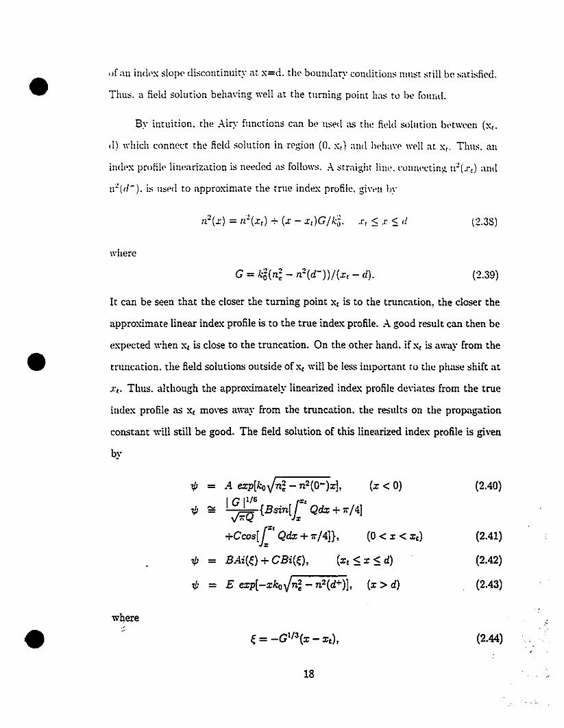
• <Jf au iud,·x slopl' discoutinuity at x=d. the boundary couditious lllUSt still bl' satisfil'd.
Thus. a field solution behm'ing weIl at the tuming point h:\$ to he fouud.
By intuition. the .-\iry functio:ls l'an be used as the field solutiou Iwtween (x"
d) which connect the field solution in region (O. x,) :\Il,l heha\'e \\'ell al. x,. Thus. au
indpx profile' liuearization is needed as follo\\"s. A straight lilll'. "ollll"cting u~(.r,) al1<1
u~("-). is llsl'd 1.0 approximate the true index profile. gi\"l'u hy
(2.38)
whete
(2.39)
•It l'an be seen that the closer the tuming point x, is to the truncation, the closer the
approximate !inear inde.'I: profile is to the true inde.'I: profile. A good result l'an then he
expected when x, is close to the truncation. On the other hand. if x, is away from the
tl'uncation. the field solutions outside of x, will be less important to the phase shift at
;1".' Thus. although the approximately !inearized index profile de\'iatcs from the true
iudex profile as X, mO\'es away from the truncation. the results on the propagation
constant will still he good. The field solution of this !inearized index profile is given
by
'if; - .4 exp[koJn~ - n2(0-)x], (x < 0) (2.40)
'if; 1G 11/6
[':::: ..;r.Q {Bsin[:z: Qdx + 'Il'/4]
+Ccos[[' Qdx + 'Il'/4]}, (0 < x < x,) (2.41)
'if; - B.4i(ç) + CBi(ç) , (XI:::; X :::; d) (2.42)
'if; - E exp[-xkoJn~ - n2 (d+)], (x> d) (2.43)
where." .• ç = _G1/ 3 (X - xc), (2.44)
18
(2.45)
• A.B.e. and E are constants, G is given in Eq.(2.39). and Ai and Bi are the Airy
functions [il. If the Airy functions in Eq.(2.42) are replaced by their asymptotic
forms, Eq.(2.41) can b.. dcduced from Eq.(2.42) [Appendi.x 1]. Matching the fields
and their derivatives at x=O and x=d leads to the dispersion equation [Appendix 2]
t=' n~ - n2(0-) .Jo Qdx = M .. + tan-I[T/i n2(0+) _ n~l + tp,
where the half phase shift at x, is given by
-1 h4i (Çd) - Gl/3A: (Çd)4>, = ../4 + tan [PdBi(Çd) _ GI/3Bi(Çd)]'
and Pd = P(x = dl, and Çd = ç(x = dl·
(2.46)
(2.47)
•
To demonstrate the improvement of this modified WKB method, a waveguide
will be taken as an example which inde.x profile is linear given by
{n~ x<O
n2(x) = n~ + (n; - nml - x/dl 0 < x :5 dn~ d:5 x
The profile is truncated at x=d. Assume the index discontinuity at x=O is large
(strongly asymmetric). Then, the half-phase change at x=O is 1r/2. Defining the
normalized frequency V and the normalized propagation constant b as
V=kdJn; -n~ (2.48)
•
Since the index profile is strongly asymmetric and !inear, the exact dispersion equation
(the field vanishes at x=O) can be found in Eq.(4.42) in [3]. The curves of b-V and
t;fl,-b are presented in Figs.2.4 and 2.5 respectively for TE polarization.
The plots show substantial improvements especially in the single mode region
and the modes near their cutoffs after the modified phase shift (2.46) has been
adopted.
•t..s shown in Fig.2.5, the clifFerences of tfi, from 1r/4 are not negligible especially
for lower order modes when the modes are near their cutoffs (b-+ 0). Sîmilar results
can also be found in Fig.2 of [8].
19

•0.8
o Exact- madified WKB
0.6 -- WKB
b 0.4
~2 • n2
0.2no
o x
0.00 2 4 6 8 10 12
v
Figure 2.4: Normalized b-V plots for a strongly asymmetric linear profile.
1.0,------ ----.•0.2
'Ir/12-m=O-- m=-1
m=2
0.2 0.3 0.4 0.5 0.6 0.7
b
•
0.0+---1----+---+---+----1-_-+-_--10.0 0.1
Figure 2.5: Phase shift dependence on the propagation constant. tPt is one half of thephase shift at Xt.
The detail of MWKB method is presented in [4]. The modified half phase shift
given in Eq.(2.46) is the special case of a truncated surface waveguide which will be
applied to Ag+ ion-exchanged waveguidein our devices later on.
20
•
•
2.5 Bearn Propagation Method
The beam propagation method (BPM) basically consists of propagating the
input beam over a small distance through a homogenous space and then correcting
for the refractive-index variations seen by this beam during the propagation step [9].
The correction simply amounts ta the application of the lens law. The result provides
a d,>tailed and accurate description of the propagation field. The method is suitable
for a dedce with a complicatEd refracti\'e-index profile and yields solutions including
not only high-order guided modes but also radiation modes (Ioss).
The method is applicable to the case of weak guidance governed by the scalar
Helmholtz wave equation. Numerically, it is based on the split operator and discrete
Fourier transform techniques. Although the method generally also works for three
dimensional problems, it will be only used to solve two-dimensional problem (e/ex =0) in this thesis work to save the computing time.
2.5.1 Theory and formula
Taking the Fresnel \va\'e equation (2.18) as an ordinary differential equation
with respect to z and letting Wn be the complete solution to the wave equation at
:: = =n, we can have the solution at Zn+l = Zn +~z in terms of Wn given by [la]
(2.49)
•
where
= J2,. 1<·+1 [n2(y, z) _ l]dz (2.50)
X ~z<. ~ ,
k,. = kon,., and n,. is a reference inde.'C. In general, the operator [j2/ ôy2 and X do not
co=ute. lt is clearly shown in [la], however, that for any analytic function X i.e.
one that can be represented as a Taylor series in z, the solution (2.49) cau be replaced
21
• with ;\ ~ecand-order accuracy by one invol\'ing the ~ymmetrized ~plit. aperatnr farm
The algorit.hm for propagating the field o\"t'r a distance .0:..: thus consist.~ of incrl'-
lIH'nr.in~ r.lll~ phase in accorrlance wirh ;\ non-uniform medium indt'x ,'hang.t'~, f,,!l'"I'l'd
by a uniform medium (n r ) propagarion of the resulting field Ol"er ;\ di~t:Ull'l' ~~, i.l',
~alving the equation. ail; i)2,j'
"Jk -- r-a - -a,".: y-l') - '»),-,"-
•
In arder to introduce the symmetrization, it is only necessary~ introduce t.he pro
cedure by a step of propagation ol'er a uniform medium (nr) from z=O to z=.0:..: /2.
In the phase correction term gil'en by -.6.':X/2kr through a distance .6..:, n=n(y,z)
can be a complicated inde., profile for which the accuracy still holds as long as n
changes slowly. This is one of the reasons why the BPM is powerful.
The numerical solution of Eq.(2.52) is obtained by expanding tj;(y,.:) in a finite
Fourier seriesM/2
!p(Y.,:) = 2: !Pm(.:)exp[j27l' n;.y] (2.53)m=1-M/2
which e.,hibics periodicity over a span of L = JvI.6.y in the y-direction. On substituting
e.,pression (2.53) into Eq.(2.52), the following e.'Cpression for !Pm(.6.z) is obtained [10J.
(2.54)
The initial values !Pm(O) are evaluated numerically by an application of the discrete
Fourier transform (DFT)
The numeriCl!1 l'valuation of Eq.(2.55) is done with the fast Fourier transform (FIT)
algorithm.•~r-l tn
'l/Jm(O) = 2: 'fi;m(tn~y, Z = 0)exp[-j27l'uMl.u=o
(2.55)
22
• Eq.(2.53) in conjunction with Eqs.(2.5-l) and (2.55) pro\'ides an exact solution
to Eq.(2.52) for an initial field of limited spectral balldwidth. In accordance with
Eq.(2.49) the propagation step is followed by multiplication of J.:,' by the phase cor
recting factor exp( -j!:>o=x./2kr), hence
(2.56)
•
•
If the spectrum of -0 remains fini te and is bounded by that of li; before the phase
correction, the Fourier coefficients "'~(!:>oz) of 1iJ in Eq.(2.53) can be e\-aluated exactly
in terms of the sampled values on the computation grid points. Then, the ne.'Ct !:>o=
propagation cau be similarly followed. In the computation, every propagation by !:>o=
consists ofa FFTconverting the field ,p(y,=) into its space spectrum u'm(=) gO\'erned
by Eq.(2.55), !:>oz propagation through a uniform medium (n,.) governed by Eq.(2.54),
and an inverse FFT converting the space spectrum back to the field 'lj;(y, =+ !:>oz).
However, to start the computation, the tirst step is a half-step propagation (!:>o=/2).
Then, it is followed by a lens operator (multiplied by a factor exp(-j!:>O=X/2"")).
To get the true field values at z = Â=, a half propagation step is required after
the phase correction. Then, another half-step propagation is needed to continue the
computation. These two half-steps can be put together as one step (Âz) to save the
computation time if there is no need of comuputing the true field at that point (Âz
here) which is often the case unIess where the field values are needed for plotting and
monitary purposes.
2.5.2 Absorber boundary
If there exÏ5ts a radiation loss in the problem wc are studying, the radiation
field will pass through the edges of the computational 'window a10ng the y-a'Cis. Since
wc have used the finite Fourier transform, this radiation field will, in the succeeding
steps, be folded back to the opposite edges of the window, causing high- frequency
23
• Illlmt'rica! instabi!itit's. In ordt'r to ,\\"oid lhis pruhlt'Ill, \\,p musl ahsorb lh,' fi<'1d al
II", l'dgt's of tht' \\'indo\\'. for t'xamp!t'. hy sl'tting tll(' dt'l'trÎl' fi<'1d al t!l<' tirst aud la.'t
fp\\' \\'indo\\' grid points ta zt'ro or by insl'rting a larg,· IH'gati\'l' imaginary l'OIllJloul'nt
in lht' rt'fracti\'l' index at tht'st' points, But it is found that a largt' alllplitud,' high
frt'qut'ncy ripple is imp!anted on tht' t'!t'ctrie fit'ld insidt' tlll' \\'indo\\' [lU], :\ suit.ablt'
absorber in tht' computation can be obt.ained if tht' electric field is Illultiplit'd by tht'
following function
{
1..J.bsorb(y) = Hl + cos1 [;r(y - Yb)/(Y. - Yb)]}'
O.
1Y 1<1 y.11Y. 1<1 Y 1<1 Yb 11Yb 1<1 Y 1<1 Yn 1
(') --)_.0,
•
where Yn is the coordinate of the grid boundary, Y. denotes the iIlIler edge of the
absorber, Yb is the outer edge. The parameters 1. Y., and Yb are chosen empirically
for each problem'5 configuration and step size to ensure that the field is absorbed
gradually over a sufficiently wide region 1Y. 1<1 Y 1<1 Yb 1·
The step size ~z is an important parameter in the BPN!. An exclusive discussion
is given in [la]. The choice of ~z is dependent on the refractive index profile. Here,
we give the range of ~z which is often used in integrated optics
(2.58)
•
2.6 Explicit and Stable Finite-Difference BearnPropagation Method
Recently, the beam propagation method (BPM) has been significantly improved
after finite-difference (FD) schemes replaced the FFT scheme. There are two kinds
of commonly used finite-difference .>chemes. One is the Crank-Nicolson method [11]
in which a tridiagonal matrix has to be found followed by finding its inverse matrix
for each propagation step. This scheme is stable and accurate. For a weakly guiding
structure, a large step-size can be used with a reasonable accuracy. However, for a
24
•
•
thn'c-dimensiona! problelll. the lllatrix becomes cOlllplicated. It will not be easy to
fine! the inverse rnatrix. The ather is simply based on an explicit (centered forward
difference) rnethod [12]. The latter rnethod gives a very simple formulation for each
propagation step. which is good for sol\'ing a three-dimensiona! problem. However.
its stability is critical. In order to keep the scheme stable, the propagation step has
to be less than a certain size which usually must be very small and, in sorne cases,
too small to be applicable.
In this section, we will present a different finite-difference scheme, based on the
DuFort-Frankel method [13] which is explicit and stable [14]. It has the merits of both
the above-mentioned methods. The scheme is not yet popular and not even mentioned
in sorne mathematical books because it introduces an c-\':tra error proportional to the
second-order derivative of the field with respect to the propagation direction. If
the structure is weakly guiding as mast cases are in integrated optical devices, this
second-order derivative is smaIl and can be neglected as usually done in deriving
the para"<ÏaI wave equation. Since the scheme is c-xplicit, it is particularly useful
for three-dimensional problems. The new scheme will be discussed only for a two
dimensional structure in this section, assuming ô/ôx =O. Please see [15] for solvÎl:g
a three-dimensional problem by the new scheme.
2.6.1 Conventional explicit FD-BPM
éPt/J",.n :::::: t/J"'+l,n - 2t/J",.n + t/J"'-l.n _ t::.y2 éJ4'I/Jm,n (2.60)ôy2 t::.y2 12 ôy4 '
we have the finite-difference wave equation for TE modes given by [Appendix 3)
•
E.xpressing the Eq.(2.17) in finite difference by [16]
_Ôt/J_m,_n :::::: t/J",.n+l - t/J",.n-l _ _t::.?__lfl-;:t/J:-:",;;,.n",ôz 2& 6 ôz3'
and
t/J",.n+l =t/Jm,n-l + r(t/J"'+l.n + t/J"'-l.n) - (1 - ar)r(2t/J""n) + Er!,
25
(2.59)
(2.61)
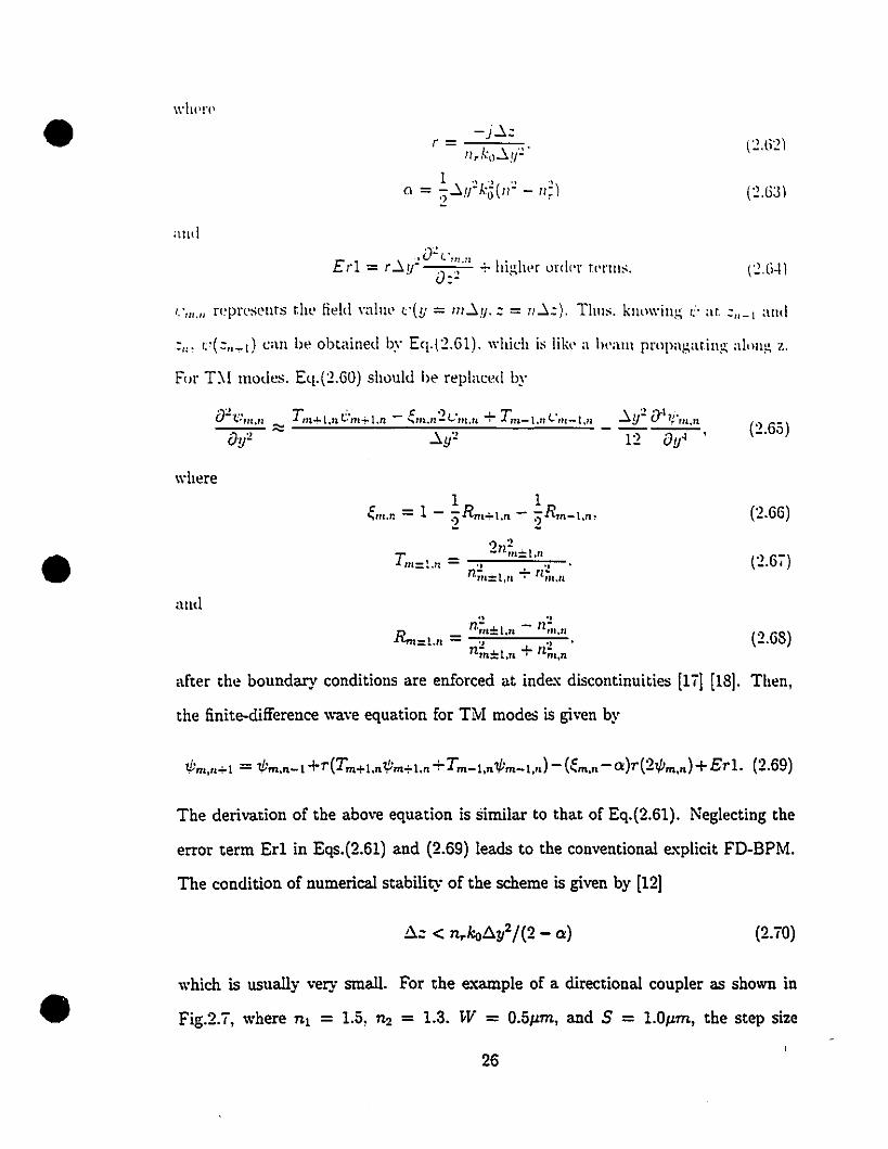
•and
l .\",' "Cl = -~tl-ko-(n- - no).) . r
(ê.Gê)
(ê.G3)
(ê.G~)
1, ·m ... repn'seuts the fidd "ainl' t'(U = lit ~.'I. z = n~=). Tltns. knll\\'in~ ". ar. =.. _1 and
,:,,, t:'(z,,-d can be obtained b~' Eq.(:2.61). \\'hiclt is lik" a lH'alll prllpa~atinp; al"n~ z.
ror T:\r modes. E<[.(:2.60) sltould be replaced by
•
D~'" T :. C·)',J. T .l,;'rtt.n == m.l.nt,;'m+l.n - .... m.n-L. m.n ' m-l.ttl..m-t.n
Dy~ ~U~
where
and
(:2.65)
(:2.66)
(:2.67)
(2.68)
•
after the boundary conditions are enforced at inde:" discontinuities [1'iJ [181. Then,
the finite-difference wave equation for TM modes is given by
'1/:m,n+1 = ·1/:m,..-1 +r(Tm+l...1,':m+I... +Tm-I,.. '1/:m-I.") - (~m,n- a)r(2'1/:m,.. )+Er1. (2.69)
The derivation of the above equation is similar to that of Eq.(2.61). Neglecting the
error term Erl in Eqs.(2.61) and (2.69) leads to the conventional explicit FD-BPM.
The condition of numerical stability of the scheme is given by [12)
(2.'i0)
which is usually very small. For the example of a directional coupler as shown in
Fig.2.ï, where ni = 1.5, n2 = 1.3. W = 0.5JLm, and S = 1.0JLm, the step size
26
• ~= < 0.00ï2W" is the condition for the numerical stability when ~y = 0.05pm.
wavclength >. = 1.5pm. and the referencc index n, = 1.3ï2 are chosen from the
average effective index of the first and second order local modes. Since Eq.(2.61) or
(2.69) is exp!icit, it is known as the conwntional explicit FD-BP:o.I.
2.6.2 Dufort-Frankel FD solutions
The relation between the second-arder derivative of field 1iJ and its centered
finite-ditference c-xpression with respect ta the propagation direction z is given by
(2.ïl)
•Solving for 2t/Jm,n in Eq.(2.71) we have
? 1 liA zfJ2Wm,n-VJm,n ~ Vlm,n+l + 1pm,n-l - .:..l= ô=2
Neglecting terms with orders higher than .6.zZ, we have
.6.z4 (}4Wm.n12 ôz4
(2.73)
(2.74)
This is the so-called Dufort-Frankel approximation. Replacing 2tPm,n in Eqs.(2.61)
and (2.69) and soh'Ù1g for field t/Jm,n+b we obtain
1- r(l- Q) rtPm,n+1 = 1 + r(l _ Q) tPm,n-1 + 1 + r(l _ Q) (tPm+I,n + tPm-I,n) + Er2
for TE modes and
./. _ 1 - rœm.n - Q) ./, + r(Tm+I,ntPm+!,n + Tm-l.ntPm-l.n) + E 2'l'm,n+! - 1+ r(~m,n _ Q) 'l'm,n-I 1 + r(~m,n _ Q) r
for TM modes, where
r.6.yZ fJ2tPm,n [ ) .6.z2] .Er2::::: 1 (1 ) ô Z 1 + (1 - Q A Z + higher order terms,+r -Q Z .:.J.Y
(2.75)
(2.76)
•where the differenœs in Er2 due to the polarizations have been neglected in
Eq.(2.76). Neglecting the error term Er2 in Eqs.(2.74) and (2.75) results in the Dufor!
Frankel FD-BPM solutions. In comparing with Er1 in Eq.(2.64), the Dufort-Frankel
27
• tD-F1 solurion has an ~rror not only dlll' to rh,' Frl'snd apprm:illlation trhe tirsr t,'rlll
in rhe square brack"t üf Eq.(:2.76) bm also ,lm' t,) thl' n,',;I,'C( of the term in th,' ord,'r
of (~=/ ~y)~(Yom.,,/D=2 (the second !l'rm in th,' squatl' bracket of Eq.(:2.76) :\llli (\
ass\llll,'d small). Ir l'an b" se~n that if ~= :5 ~!I. r.his l'xtra .'rror will hl' l'l]ui\"all'nt
Il l'an lw sho\\'n rhat rllt' D-f ,,)lutions are \"on :\l'Ulnann sr.abl.. :.-\Pl'l'ndix .lj
if the rdracriw index n(y.2) is tl'al and
Tl r~= :5 ~y where' n(y.:) > " r ./., .,
Vn- - n;:( .) --)_.l' ,
•
•
For n(y. =) ::; llr. the scheme is unconditionally stable pro\'ided that n(y.2) is l'l'al.
Il. is \\'orth ta point out that the condition of (:2.11) l'an al\\'ays be satisfied if the
reference index nr is chosen te be or close to the ma:I:imum of n(y, :).
2.6.3 Leap-frog ordering of calculation
Taking a close look at Eqs.(:2.14) and (:2.15), it is not difficult ta find that
O".,n with an l'ven number m = 2.4;", arc independent of the pre\'io\ls field V'alues
~~·"..n-l \\'ith an l'ven number m = 2,4;", and the next previous field \'alues ·t/J".,n-2
with an odd number m = 1,3,..·. Thus, we l'an ha\"e two independent sets of solutions
indicated by circles and solid dots respectively in Fig.2.6. Usually, one set is enough,
for example, the circles. Thus, the field values at the solid dots are not needed and the
amount of computation time can be reduced by half \Vithout decreasing the accuracy.
This is called the leap-frog ordering of calculation [13].
28
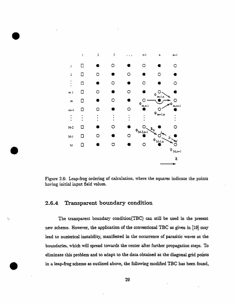
•~ ) n·' n n-'
0 • 0 • 0 • 0
~ 0 0 • 0 • 0 •0 • 0 • c • 0
m·1 0 0 • 0 • O~,~ •'" 0 • 0 • O~-O
o /0. m.n-1 . m.n... 1
",·1 0 0 • 0 • 0 •$m... l.n
~I·:: 0 • 0 • Ok. 0lb ~
0 0 • 0. M·~n·1 (-.,...
~I·I • 0 .•o ~: ~t.l.n ~
~I 0 • 0 • o • 0• Cl~t.n ... 1
Z
•
Figure 2.6: Leap-frog ordering of calculation, where the squares indicate the pointshuvillg initial input field values.
2.6.4 Transparent boundary condition
•
The transparent bounda.r:r condition(TBC) cau still be used in the present
new scheme. However, the application of the conventional TBC as given in [19] may
lead to nunierical instability, manifested in the occurrence of parasitic waves at the
boundaries, which will spread towards the center after further propagation steps. To
eliminate this problem and to adapt to the data obtained at the diagonal grid points
in a leap-frog scheme as outlined above, the following modified TBC has been found,
29
•t,,'.\l.n-l = t>~[_l.n/t:·.\f_:.:.tl_l' (2.7S)
which is a modified form of the conwntional TBe
t"'.\!.r:-l/V.\l-l.tl = L'.\t-l.n.o..I/t..:'.H-::.r1(::::: l'.\l-I.'I/l'.\l_::.II_I). (2.79)
Tl) ('U:-itU'(' Ol1tg,Oillg. wa\"es o1l1y. the iluagillary pan üf fO!lf" (t'.\! -1.'1.1 t.'.\t -:':.11 -1) [ ~.B.
1'.II_l.n = 1;··.\I_~.n_lexp( - jk,s). k., is the wm'enumber along the diagonal direction.]
should be negative.
2.6.5 Example and comparisons
•The slab wa\'eguide directional coupler as shown in Fig.2. j has been taken as
an example ta illustrate the new scheme.
,.W'il
1
: S=1.0 J.l.ffi1
*
~z
À=1.5J.l.ffi ------------'f\~-1
, W=O.5J.l.m
~
•Figure 2.ï: A schematic diagram of a para1lel slab \\"a\"eguide coupler.
The \\"avelength ,\ is 1.5~m and the window size is 10J.L11l. Thus, Eq.(2.77)
gives b.z $ 2.3~y for stability. Assume ~y = 0.05~m. In the new scheme, t:.z $
30
• ~!J = O.OSwn is required to keep the extra error term insignificant and hence the
results equally accurate, which is about ï times of the step-size of Eq.(2.ïO) in the
conventional explicit scheme.
0.4 .......--------------------,
0.3 F-.--'--..--"--'.--.__.. __.. __..~..__..__. __. __..__..__..~..__ .
~y =0.05 JI-rrl0.2
0.0 F'':,.:.''.:.;.''.:.,:''..:.;.'c:..'."".:,.:.'• .:.;.'•.:..;''..:.,:'.~••
0.1...o......w
èll! -0.1
~y =0.0 1 JI-rrl
-0.2
-0.3 . . .. Cronk-Nicolson- DuF'ort-F'ronkel
1.0000.1000.010-0.4~-~---...-.j-_--..l--_+_--I.---__1
0.001
•Step size l!.z (}.un)
Figure 2.8: Fercentage errors in the coupling length versus the step-size ~=. Theother parameters are given in the text.
•
Fig.2.8 shows curves of the percentage error for the coupling length versus the
propagation step-size ~= for TE polarization. lt can be dearly seer. that the error
is mainly dependent on t:.y when t:.= ~ Ây and the error increases dramatically for
Â= ~ 3Ây. However, it is still reasonable for t:.z =2t:.y which is 14 times that allowed
in the conventional e.'Cplicit method. Although the propagation step-size is restricted
by the stability requirement Eq.(2.ïï), the extra error term (ÂZ/Ây)2éPrPm,n/Ô~' is
the main reason for limiting the step-size according to our experiences. The coefli
cients in front of the field values on the right side of Eq.(2.ï4) are slightly more com
plicated than those in the conventional e.'Cplicit scheme Eq.(2.61). Without worrying
about this minor difference, the ne\\' scheme with the leap-frog ordering technique can
be potentially about 27 times faster than the conventional e.'\,-plicit scheme in compu
tation for this particular example if Âz = 2Ây is taken as the step size. Comparing
31
•
•
•
\\"irh rlll' ..rrur in the Crank-:\icolson metho,l. some impro,·..nlt'IH. is sllllwn in Fi~.:2.S
whil'h lllay b.. due to the use of the ne\\" transparent bUllndary condition Eq.(:2.7S).
Lertin~ ~!J = L'.Olllm am! l:encc ~.: = :2~!J = 0.0:211111 in bot h rh,' ne\\" Sl'h,'nH'
anel the Crank-Nicolson schenw. wc performl'd the computations for the l"Ollplt'r with
·lOl"TI in len~th on a Sl':\' SPARC station. The cpe rimes are 1-1:3 s''''onds and 7:lll
s('('onels fur the tH"': and Crank-:\ieolson SChellll'S [t·spectiwly. ke"pin~ it in mind r.har
rh.. ~rep-size~.: in the Crank-Xieolson schellle is not subj,'cted to the same limiration
of ~.: = O.021.11n.
The ne\\' scheme is explicit and stable. It can be easily implemented into a three
dimension FD-BPM [15]. The propagation step-size can be at least the size of the
transverse grid. \\'hich is much larger than that in the com'entional expl:cit scheme.
'Vith the leap-frog ordering technique, the ne,,' scheme can be more efficient. The
new scheme was "ery recently de,·eloped. Only a newly proposed three-\\"lIvelength
demllitiplexer (sel' Chapter 7) has benefited l'rom the highcr tllmwricai dliciency.
Fortunately, other devices are shorter and narrower and, hence, l'an be adequately
treated \\'ith the FFT-BP)'!.
2.7 Effective Index Modeling
50 far the methods "'e presented are ail for two-dimension problems. In this
section, we will present the weil known effective index method to simplify a threp.
dimensional problem to two two-dimensional problems [20] which, in tum, ;can be
solved by the methods introduced in previous sections. Since the refractive inde.'C
profiles of ion-e.'Cchanged surface glass waveguides are slowly varying, the scalar wave
equation Eq.(2.ï) can be used and a reasonable assumption Ilt(x, y, z) = X(x)cp{y, z)
32
• can b" adopted. This assumption transforms the scalar wave equation into
1 82X(x) , 1 [8
2, 8
2]"'( .). k2' 2( _) 2 ( • l' 2 ,
""" I( , ) 8 """"8 o"i' y.• """ oln X·Y._ -ne!! y.•) """kone!!(y·::) = 0"(x) 8x2 () y .•- y- :;--,. .(2.80)
where ne!!(y. z) is the lateral effective index profile function and will be discussed
more later. Eq.(2.80) can be divided into two equations
for the lateral problem along y. If a channel waveguide is considered. the refractive
index is uniform along z. Then, the substitution of <I>(y. z) = t/;(y)exp( -j{3z) into
Eq.(2.82) leads to
•
ô'X(x) O[ "( ) ? ( )] '( )ax' + ka n- x. Y.:: - n;1I Y. z X x = 0
for the depth problem along x and
ô't/>(y) k?[ 0 () ?J"'()ôy' + + an;1I y - n; "i' y =O.
(2.81)
(2.82)
(2.83)
where ne = (3/ka as the effective inde:\( of the propagation constant. If the index
slowly varies along z, the expression <I>(y.z) = t/;(y,z)exp(-jn,.z) should be used to
obtain the Fresnel wave equation after (f2t/>/ôz2 has been neglected
(2.84)
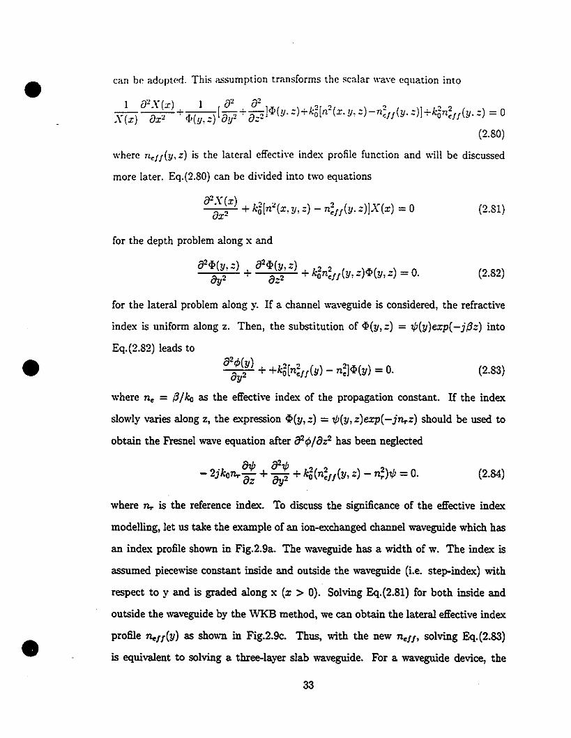
•
where n,. is the reference index. To discuss the significance of the effective index
modelling, let us take the example of an ion-exchanged channel waveguide which has
an index profile shown in Fig.2.9a. The waveguide has a width of w. The index is
assumed piecewise constant inside and outside the waveguide (i.e. step-index) with
respect to y and is graded along x (x > 0). Solving Eq.(2.81) for both inside and
outside the \vaveguide by the WKB method, we can obtain the lateral effective index
profile n.1I(y) as shown in Fig.2.9c. Thus, with the new nell' solving Eq.(2.83)
is equivalent to solving a three-layer slab waveguide. For a waveguide device, the
33
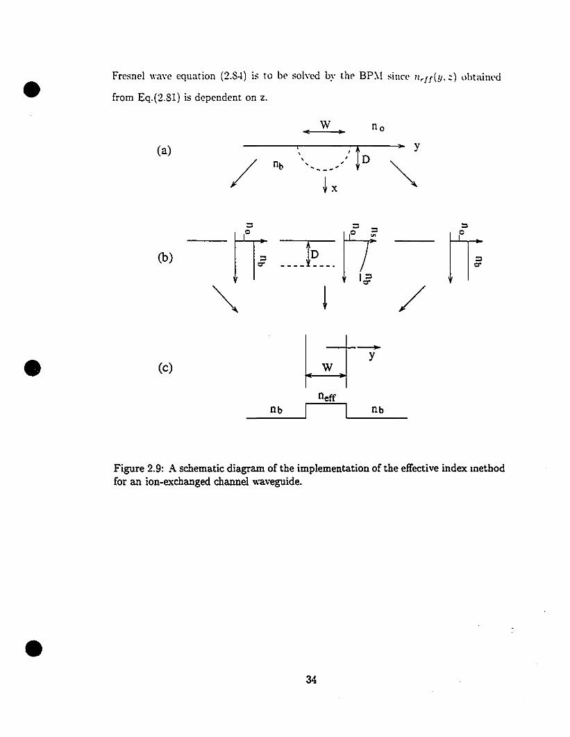
• Fresnel waye eqllation (2.8-1) is to be sol\"Cd by the BP:'! sillet' Tl,If(Y.;) obtailll'd
from Eq.(2.81) is dependent on z.
wE J'
(a)
/i ! ,y\" ,': D '"
~-~ ~
~ x
r1; Jt::l
JI;(b) ~ ___J~__. I~
~ ! /
• (c) ~Yneff
nb nb
Figure 2.9: A schematic diagram of the implementation of the effective index methodfor an ion-exchanged channel waveguide.
•34
•
•
•
Bibliography
LI: R.'·. Ralllaswamy amI R Sri\'asta\,t, "Ion-exchanged glass wavegllides: a review·· .
.1. Lightwave Technol.. \'01. LT-G. pp.98-1-1001, 1988.
[2] .J. Heading, .'ln introduction to phase-integral methods, Methuen, London, 19G2.
[3] ::tU. Adams, An Introduction to Optical Waveguides. John "Viley and Sons,
Chapter -1 and 5, 1981.
[-11 F. Xiang and G.L. Yip,"A modified ","KB method for the improVl'd phase shift
at a turning point", IEEE Journal of Lightwa\'e Tecllllology, vol. 12, ppA-I3-452,
::tlarch, 1994.
[5] A.H. Hartog and M.J. Adams, "On the accuracy of the WKB approximation in
optical dielectrical waveguides", Optical and Quantum Electron., vol.9, pp.223
232,19ii.
[G] ::tI. Belanger and G.L. Yip, "A passive three-branch optical power divider in
LiNb03", Fiber and 'Integrated Optics, vo1.5, no.1, pp.65-i9, 1984.
[il NI. Abramowitz and 1. Stegun, Handbook of Mathematical Functions. Dover pub
lication Inc., New York, tenth pnnting, Chapter 10, 19i2.
[S] R. Srivastava, C.K. Kao, and R.V. Ramaswamy, "vVKB analysis ofplanarsurface
waveguides with truncated inde."t profiles" , Jouma! of Lightwave Technology, vol.
LT-5,No.n, pp.1605-1609, November 19Si.
35

•
•
•
[9] :--I.D. Feit and J.A. Fleck. "Light propagation in graded-index optical liber". Appl.
Opt.. \'01.1 ï. ~0.24. pp.3990- 3998. 19ï8.
[10] L. Thylen. "The beam propagation method: an analysis of its applicability". Opt.
Quan. Electron., vol. 15. pp. 433-439. 1983.
[l1J Y. Chung and N. Dagli. "A assessment of linite difference beam propagation
method". IEEE J. Quautum Electron., \'01. 26, no. 8. pp. 1335-1339. 1990.
[12] Y. Chung and N. Dagli, "Explicit linite difference beam propagation method:
application to semiconductor rib waveguide Y-junction analysis" Electron. Lett.,
vol. 26, no. 11, pp. i11-iI3, 1990.
[13] E.C. DuFort and S.P. Frankel, "Stability conditions in the numerieal trea~ment
of parabolic differential equations", Math. and Other Aids to Comp., vol. i, no.
41, pp. 135-153, 1953.
[14] F. Xiang and G.L. Yip, "An Explicit and stable linite differenee 2-D beam propa
gation method", IEEE Photon. Technol. Lett., vol.6, no. 10, pp.1248-1250, 1994.
[15] F. Xiang and G.L. Yip,"An Explicit and stable linite differenee BPM for ap
plications to deviee analysis and design", Conference proceedings, International
Symposium on Guided-Wave Optoelectronics, New York, Oct., 1994.
[16] P. Duchateau and D.W. Zachmann, "Partial differential equation", Schaum's out
line series, MeGraw-Hill, 1986.
[1i] M.S. Stern, "Semivectorial polarised linite difference method for optieal waveg
uides with arbitrary index profiles", IEE Proe., Pt. J, vol. 135, no. 1, pp. 56-63,
1988.
36
•J ~ \\',P, HUilllg. cr.. XU. S.T. Chu. alld S.K. Chaudhuri. ".-\ \"h 'or Iwam propa-
gal iOIl Il ... r.hod for :;uidf'd-\\'il\'l' opr.ics". IEEE PhotOll. T"chllol. Leu.. \'01.:3. no
III. pp. DIO-Dt:;. la!J!.
[I!Jj G. R. HadJey. "Transparent boundary conùition for Iwam propagatioll". Optics
LI'11 .. \'01. 16. no. 0. pp. 62~-G26. 1!J!J1.
[~lJi G.13. Hoeker aud \\".K. Burns. ":-'Ioùe dispersion in difiused channel \\',\\'eguiùes
"." t.h" Efieet,i\'e index method" ..-\ppl. Opt. .. \'01. 16. pp.ll:3-118. 1077.
2.8 Appendix
2.8.1 Deduce Eq.(2.41) from Eq.(2.42)
The asymptotie forms of Airy funetions are gi\'en by
• .-1, ::::: (2vf:7~l/-l) - i f.rp[ -(2/3)çJN] for ~ > 0 (2.85)
Bi ::::: (vf:7~lil)-le.z:p[(2/3)çJ/2] for ç > 0 (2.86)
Ai ::::: (filçll/4)-1sin[(2/3)lçI3/2 +;;/4] for ç < 0 (2.87)
Bi - (filçll/4)-ICOS[(2/3)lçI3/2 + rr/4] for ç < 0 (2.88)-For x < x" ç < 0 (see Eqs.(2.39) and(2.44). Replacing the Airy function ia Eq.(2.42),
\\'t' ha.,·c
If the index slope at X, is approximated by G given by Eq.(2.39), we can use Eqs.(2.38)
and (2.44) for X < x,, Soh'ing (x - Xl) l'rom Eq.(2.38) and using Eq.(2.22) , we have
•Thcn
37
(2.90)
(2.91)
• "Il'!
Sllbstit.lltillf\ r.hl' ab,wC' two <,qllatiolls inrD Eq.l~'S!.l), \\'t' Dbrain E'I.l~.·11 \. wltidl
Illl'alls rltat Eqs,(~.-Il) alld (~ ..l~) satisf\' tht' nlt\tlt'I't.illf\ l'Dllditilln ar .1'1.
2.8.2 The dispersion equation (2.45)
.-\t x=o, letting the field and its derÎ\'ati\'(' l'llIlrinlll' (SI'" Eqs.l:!.·Il))·l~"I:))) lt'"ds
1 G I l .'6.-1. = ~ {Bsin[S1 + ../-11 + Cr-vs[12 + .. j.l]
"Gd
and
(:!.!.l3)
• l'I'sp"l'ti\'e!y, Sol\'ing the ratio -CjB from abo\'l' t\Vo <,quations. \v<' !Ul\'l'
where
C psin(S1 + .. /-1) + cos(S1 + ../.l)- B = pcos(S1 + ../4) - sin(S1 + .. /-1) (2,95)
At x=cl, ~ = ~d, we have
p =1)1
') ')
n~ - 710-? ?
n(j+ - n~
(2.96)
and
(2.9;)
(2.98)
•Sol\'ing -C/B from the abo\'e t\\'o equations, we have
38
(2.99)
E'I",,'i!l;.\ 12.9')) and (2.99) and doin:.; some algebra lead the following equation
or =
trlll(\l - ;:' !-l) =•.-\s n'sulr.. wp ha\"(~
p"'"'11 - IHItrm(tan-1p) + trm(trw.-I'I)
1 - tan(tan-1p)trw(trw-I'I)
or = tan(tlm-1p + tan-l'Il. (2.100)
(2.101)
(2.103)
(2.104)
•
•
Titus. subsr.it.uting P.. p. anù q in Eq.(2.101) by Eqs.(2.2; '. (2.96). anù (2.99). respec-
tinol.\". IVe !"an obtain the dispersion equation (2.-15).
2.8.3 Derivation of Eq.(2.61)
L'sin;!; Eq.(2.59) for8li;/8z and Eq.(2.60) for 821f;/8z2 in Eq.(2.1i) at (y = Yrn. Z = zn),
ln' han'
(2.102)
~[ultip[ying jb.=/kon,. on both sides of above equation and using the notations of
Eqs.(2.62) and (2.63), the above equation can be reduced to
b. " 82'I/Jrn.n ( • b.z3 83'I/Jrn,n-r' Y· 8=2 + r 'l/Jm,n+1 - 'l/Jm,n-II - 3 8z3
, (/ _ ? 1 ...... 1 ) + b.y4 ~'l/Jm,n _ r ?I, - 0T r 1Vrn+I,n -1Vm,n' 'Pm-I,n 12 8y4 Q-'i'm,n - •
Therefore
'l/Jm,n+1 = 'l/Jm,n-I + r(Wm+l,n + 'l/Jm-I,n) - (1 - a)r(2'I/Jm,n)
821f: l éf''I/J r 84'I/J+ r "y2 . m,n, "z3 m,n ~y4 m,n
.:..> ~=2 -r- 3':"> 8z3 - 12 8y4'
Taking the last two terms as higher oder terms and e.'Cpressing the error by Erl given
in Eq.(2.64), we derive Eq.(2.G1) from the above equation,
39
• 2.8.4 Von Neumann stability condition
L"t l'm.n = Ccxp(jllm). ",here 'I is real. Sllbst.itutin~ it into Eq.(2.7·1) and
ncglecting Er2. we have
1-1'(1-,,)= Cll - lf )'I'"
l+r(l-n)'l'
'. <"(,Jf/rIt .)'1 ~.}111l .-J")1 · (1 )' '."~,. - n
OI"
•
.,l-r(l-a) l'E- = + ~2CU""'I·
l+r(l-a) l+r(l-u)
Sol\'iug ~ leads
~ = 1 [rcos1} ± Jr~cos21J + 1 - r~(1 - aPI.1 + 1'(1 - a)
Assume the medium is lossless and defiue
Thus. 1. is real and the square roor. in Eq.(2.106) cau be expresseù by
VI "(1 )., ., ,+ t- - a - - t-coS-II.
Set a condition
11. can be simplified ta
(2.105)
(2.106)
(2.107)
(2.108)
(2.109)
•
Since a is usually small, the second term on the right side of (2.109) can be ueglected.
Replacing t and a \Vith Eqs.(2.10ï), (2.62), and (2.63) we have the condition given
by
(2.110)
40
• Obviously. if ni!). =) S nr • the condition can always be satisfied and if nt!). =) > nr •
the condition becomes
(2.1ll)
Thus. if the medium is lossless and the condition (2.111) can be satisfied. the square
root in Eq. (2.106) is real. Then
(2.112)
•
•
which means that the scheme is Von Neumann stable. The scheme is unconditionally
stable for n(y, =) S nr and a lossless medium.
41
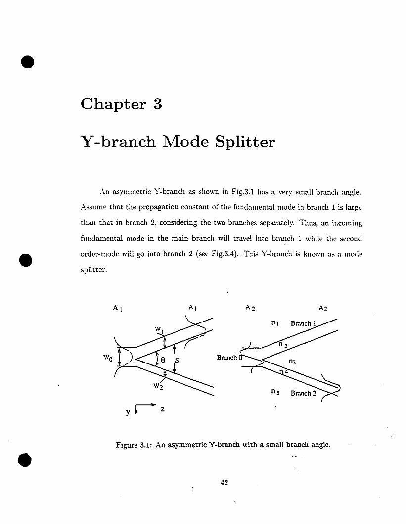
•
•
•
Chapter 3
Y-branch Mode Splitter
An asymmetric Y-branch as shown in Fig.3.1 has a \'ery small brandI angle.
.-\ssume that the propagation constant of the fundamental mode in brandI 1 is large
than that in branch 2, considering the two branches separately. Thus, an incoming
fundamental mode in the main brandI will trave! into brandI 1 while the second
order-mode will go illto brandI :2 (see Fig.3A). This Y-branch is known as a mode
splitter.
AI
Figure 3.1: An asymmetric Y-branch with a small branch angle.
42
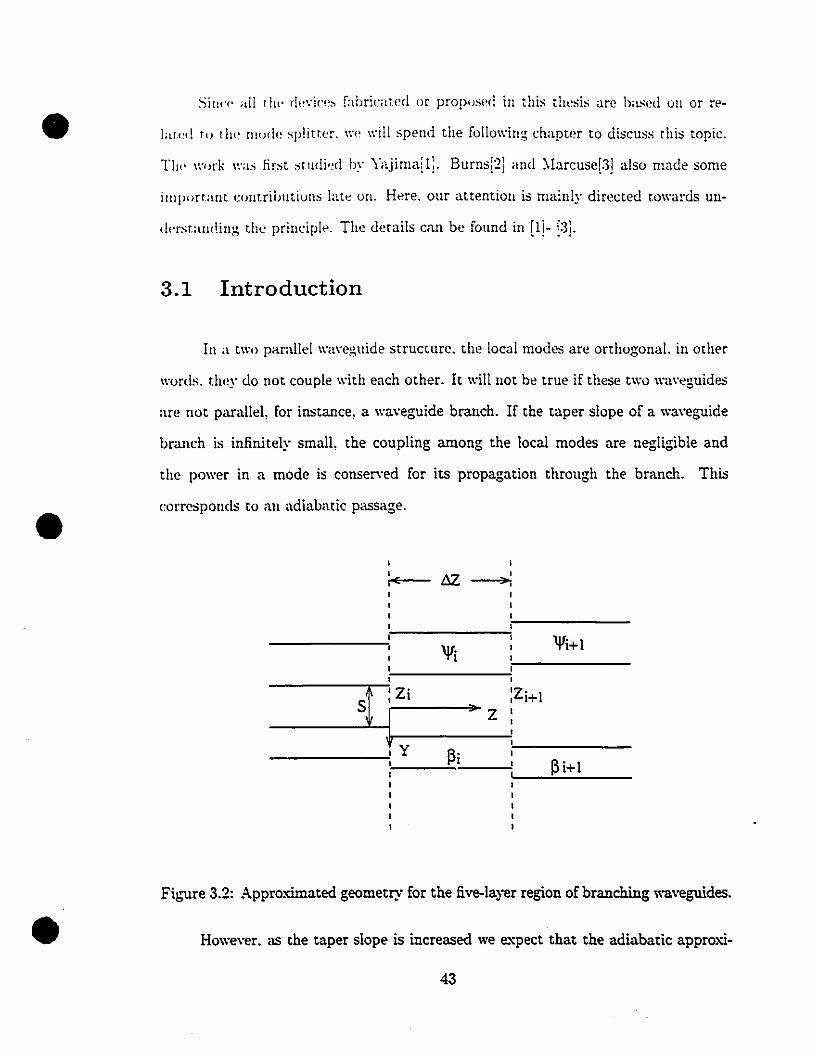
•
•
•
Siun' 'Ill th" rl"\'jn" fabricarerl or proposerl in this thesis arc bascd on or re-
la!.ed ro th,' mode splitr.er. \\'(, will spenà the following chapter to di5cu5s thi5 topic.
TIlt' work was first studi"rl by Yajima[l:. Burn5[:2] and :'larcuse[3] also made 50me
illiponant contributiuns late on. Here. our attention i5 main!y directed towards Ull-
d,·rst.anding the principle. The ùerai!5 can be founù in [1)- [3].
3.1 Introduction
ln a two paralle! "';n'eguide structl1l'e. the local modes are orthogonal. in other
wonb. they do not couple \\'ith each other. It \\'ill not be true if the5e t\\'o \\'a\'eguide5
are not parallel, for instance, a \\'aveguide branch. If the taper slope of a wa"eguide
branch is infinitely smalt the coupling among the local modes are negligible and
the power in a mode is consen'ed for its propagation through the branch. This
corresponds to an adiabatic passage.
1'l'i+1
'l'i,,1
1sqZi :Zi+l" Z 1
11
1,y~i
1,~i+l
Figure 3.2: Approximated geometry for the five-1ayer region of branching waveguides.
However. as the taper slope is increased we expect that the adiabatic approxi-
43
•
•
mariull \\"ill break cl0\\"n and a po\\",'r rmll~f,'r \\"ill ,)t'cur frlllll an input lIhH\t' lu ,Hlwr
guid,'d al1<1 radiation mode~. both transmiupd and n'ft,·t't,·,!. Thi~ pr,)hl"lIl cali bo'
"ull\'\~llieml" treated b,' the sten appruximatiull lI]<,th"d uf ~lan:II~., ;:;:. Th., ,""1tiIl1l-. . . . .
\lUS bmndt taper is approximated by a. series of discominllous. abrupt st,·p~. ~,'paratP,1
by regions of para.llel fi"e-Iayer \\"awguide al'ter the apex l~ee FiO!,.3.~).
the rransmitted mode amplitudes by reqniring the trans\'\'rs,'-lidd \'llmp"n"!ltS rD Il<'
continuou~ at the step. By breaking up the taper iuto a larg" nllllüwr of slllall steps
and repeating thi~ proce~s at each step. a reasonable approximatioll to th,· dfect of a
giwn taper slope is obtained.
:\Iode propagation is assumed in the z direction. The y direction i~ normal
to the wawguide layers, and fields and geometry arc a~sllmed llnchanged in the x
direction. The di~persion eqllation of thi~ fi"e-Iayer planar wawgllide for TE modes
is gi"l'n by [1]
\oVe restrict our attention to two transverse electric guided modes. the first and
second. The electric fields for the guided modes can be writtcn as
•
{(Oit + -13)"'2 + (-rt'Y3 - "!i)tan"!2lL'1}
'{b + 'YSh'4 + (-r3'YS - 'Y~)tan'Y4w2}
-exp(-2"'3S){(-r3 - "'th'2 + (-rt'Y3 + 'Y~)tan"i2Wt}
'{(-'3 - "{shI + (-r3'YS + 'Y~)tan'Y4w2} = 0,
where the tran~verse wave number
'YI = ko}1 n; - n; l, 1=1,... ,5.
e: = E(z)1/;(y, z)exp( -ja:(=))
44
(3.1)
(3.2)
(3.3)
• where
oc(=) = .3= + O. (3.4)
•
E(z) is the real amplitude at a point z, l!J(y. =) the real, y dependent local-nonnal
mode field distribution, and if> a phase constant. Boundary conditions for TE modes
require ez and hy to be continuous across a step at z, which leads to
and
/31iEIil/iliexp( -jocli) + l32iE.1i7/J2iexp(-jOC2i)
-/3IiE~tPliexp(joc~)- /32;E~1/J2;exp(joc~) + hre'
where the first subscripts 1 and 2 are used to denote the order of the modes, the
second subscripts i and i+1 are for the incident and transmitted fields across the step
respectively, ER is the amplitude of reflected guided modes, eTe, and hTe' represent
rellected radiated modes, and etT...... and htT...... transmitted radiated modes. We define
an overlap integral as
11"I,{'1 = Jt/J1"ItP('1dy, p,ç = 1,2 and q·71 = i, i + 1, (3.7)
•
where the integral covers the range of y where fields are not zero. A mode amplitude
(E') is introduced for the normalization, which corresponds to a mode power of unity.
At any point z, E' is related to mode power (P) by
..jP,.,q = 1 = E;,qV~11"I,pq, p=I,2 and q=i,i+l.C:C (3.8)
By using the mode orthogonality in both ~s.(3.5) and (3.6) and keeping only the
first order terms based on t1:le assumption of a sma1l step, we obtain the following
45
'.
• equaticn
where
(3.10)
IS the ratio of mode amplitude in the presence of mode cOll';ersioll to that. mode
amplitnde \\"hich corresponds to unity power. The coefficient Cl.~ is giWll by
(3.11)
•
and C~.2 can be obtained by substituting 2 for 1 in Eq.(3.11). Cp.{, (p, ~ = 1,2),
represents the coupling of power from the mode p in "i" region to the mcde ~ in
"i+1" region.
The real and imaginar:; parts of Eq.(3.9) then completel:; descrihe the trans
mitted mode 2 in terrns of the input modes.
tan~' _ CI,2.41,isinQI,i + C2,2.42.isinQ2,i'-'2,&+1 - .
CI,2AI,iCOSQI,i + c2,2A2,iCOSQ2.i
(3.12)
(3.13)
•
Since the, notation for mode 1 and 2 are symmetric, exchanging 2 with 1 in
Eqs.(3.12) and (3.13) gives .4I,i+1 and QI.i-;,l' JUter obtaining the "A"s aIld "Q"S,
we let the two modes propagate over a distance Z;+I - Z; to the next intersection at
Z = Z;+I by multiplying fields of the first-mode with exp(-iPI,i+I(Z;+1 - Z;)] and of
the second-mode with exp(-i/32,i+I(Z;+1 - Z;)] to get the fielâs just before the next
step.
46
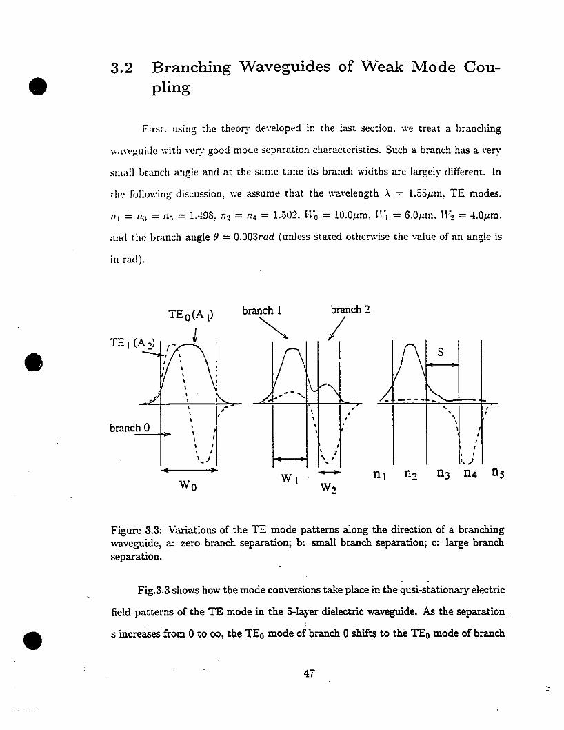
• 3.2 Branching Waveguides of Weak Mode Coupling
first. lIsing the theory de\'ploped in the last section. we treat a branching
Wa\'pi-\lIide with \'ery good mode separation characteristics. Such a branch has a very
small brancil angle and at the same time its branch widths are large!y different. In
rlit' rollowing discussion, we assume that the wa\'elength ,\ = 1.551lm. TE modes.
/II = n:) = fto = 1.-198. HZ = Il. = 1.;:;02. H'o = 1O.Ollm. 1ri = 6.0ILlU. I-\O"z = -I.Ollm.
and rhe branch augle B =O.003rad (unless stated othen\'ise the \'alue or an angle is
in rad).
TEO(A 1) branch 1 branch 2
~ /TE 1(A~) f'
1• \,\
\,\ ",,, , , , ,
\ , \ , , ,\ \ , ,
branch 0 \\,\ ,,
\ 1\ ,
1,1
\ 1 1 1\ 1 \ 1 1 1\,/ , ,
.... .1,• • ......... ni n2 n3 n4 nsWIWo W2
Figure 3.3: Variations of the TE mode patterns along the direction of a branchingwaveguide, a: zero branch separation; b: small branch separation; c: large branchseparation.
•Fig.3.3 shows how the mode conversions take place in the qusi-stationary electric
field patterns of the TE mode in the 5-layer dielectric waveguide. .~ the separation .
s incrcaSes'from 0 to 00, the TEo mode of branch 0 shifts to the TEo mode of branch
47
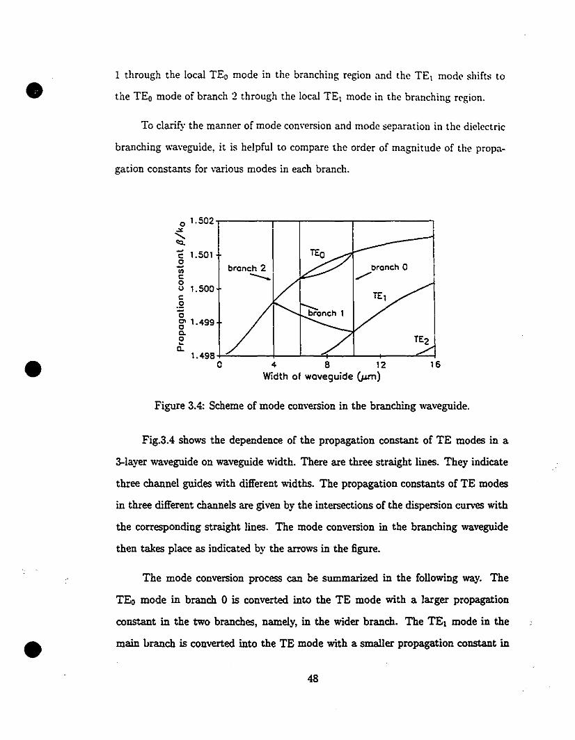
• l through the local TEo mode in the branching region and the TEl mode shifts to
the TEo mode oi branch 2 through the local TEl mode in the branching region.
To clarify the manner of mode conversion and mode separation in the dielectric
branching waveguide, it is helpful to compare the order of magnitude of the propa
gation constants for various modes in each branch.
16
Dranch 0./
4 8 12Width of woveguide (}Mn)
branch 2---
1. 498 .j-:':.----l--.J---':+-_.J-__-~""-_l
C
o 1.502..-----r---,----...,.-------,
""~C 1.501BUlc:ou 1.500c:.2ëgo 1.499c-o~
a.
•Figure 3.4: Scheme of mode conversion in the branching waveguide.
Fig.3.4 shows the dependence of the propagation constant of TE modes in a
3-layer waveguide on waveguide width. There are three straight lines. They inclicate
three channel guides with c1ilferent widths. The propagation constants of TE modes
in three dilferent channels are given by the intersections of the dispersion curves with
the corresponding straight lines. The mode conversion in the branching waveguide
then takes place as indicated by the arrows in the figure.
•The mode conversion process can be summarized in the following way. The
TEo mode in branch 0 is converted into the TE mode with a larger propagation
constant in the two branches, namely, in the wider branch. The TEl mode in the
main ùranch is converted into the TE mode with a smaller propagation constant in
48
the two branches.namelv. in the narrower branch.
It is Ilseful to note that the mode conversion mechanism in the branching waveg
Ilide can be explained in terms of the adiabatic theorem, which describes a motion
in sorne dynamical state with slowly varying external parameters called adiabatic
ill\"ariants. In the mode conversion process in the branching waveguide, the state
is represented by a propagating wave in a part:~ular mode through the multilayer
waveguide with a slowly varying separation between the two branches being the e:'{
ternal parameter. In this case, the adiabatic invariants are the mode number and
mode energy. This means t!Jat the TEo mode, for instance, in branch 0 in Fig.3.1
remains, as it proceeds, to be the TEo mode in the multilayer waveguide to the right
hand side, although the shape of mode pattern looks like the TEo mode associated
with either branch 1 or 2.
•
• 3.3 Dependence of Branch Parameters
•
The discussion in the last sub-section is for an ideal Y- branch. If the branch
angle is not that small, the adiabatic invariants will not be weil preserved and mode
conversion will not be completely in the direction as indicated by the arrows as shown
in Fig.3A. Mone coupling will occur.
As a mode splitter, we expect the norrnalized amplitude AI to be close to unitY
and A2 close to zero when the TEo mode in branch 0 is converted into the 'TEo mode
in branch 1. Two branch parameters, the branch asymmetry and the branch angle,
affect. the performance most as concluded in [1) and [2). The branch asymmetry
includes the branch geometry and branch index.
Taking the same parameters as given in the last section, but choosing'8 = 0.01
and three dilferent branch width combinations as, (1) Wo= 10.0~, W1 = 6.5J.i"m, and
49
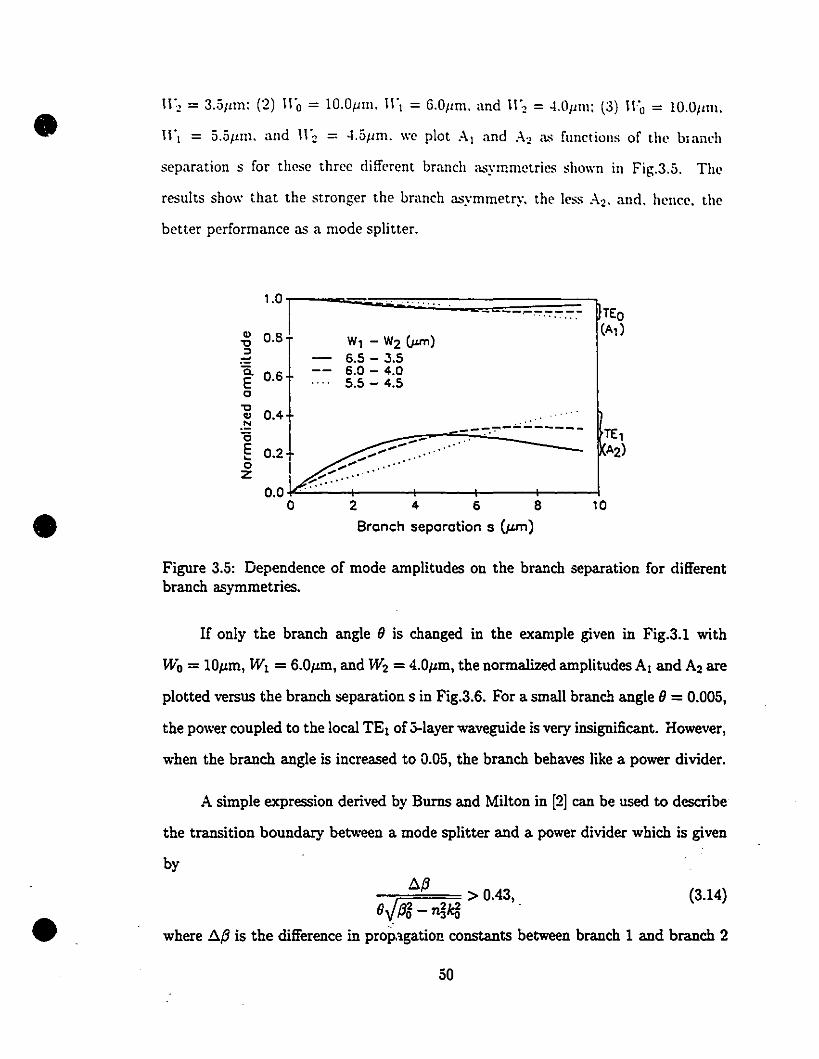
• 1r2 = 3.51Im: (2) Iro = lO.O;.nn. \1"1 = G.Ollm. and 1r2 = 4.0Jl111: (3) \Fo = lO.OIHn.
\1"1 = 5.5ItIU. and 1r2 = 4.5Ilm. we plot AI and A2 11-< fnnclions of the blanch
separation s for these three different brandi asymmetries shawn in Fig.3.5. The
resnlts show that the stronger the branch asymmetry. the Jess A2 • and. hence. the
better performance as a mode splitter.
1.0
1 =-=--~--- - TEO...... '"
., (A, )"tl 0.8 W, - W2 (}un)
" 6.5 - 3.5::Q. 0.6 6.0 - 4.0E 5.5 - 4.50"tl
0.4.,•!:! .. ' .
--~.":""'-------- TE,"6 --E 0.2 -- A2)... -- ."0 -- .. '
z ~-:.--:.~... "" .0.0
0 2 4 6 8 '0• Branch separation s (Jun)
Figure 3.5: Dependence of mode amplitudes on the branch separation for differentbranch asymmetries.
If only the branch angle 9 is changed in the exampJe given in Fig.3.1 with
Wo = lO~m, W I =6.0~m, and W2 =4.0~m, the normalized amplitudes Al and A2 are
plotted versus the branch separation s in Fig.3.6. For a small branch angle 9 = 0.005,
the power coupled to the local TEl of 3-layer waveguide is very insignificant. However,
when the branch angle is incre.ased to 0.05, the branch behaves like a power divider.
A simple expression derived by Burns and Milton in [2] cao be used to describe
the transition boundary between a mode splitter and a power divider which is given
•by
f).{J> 0.43, (3.14)9v.{J~ - rl5kfJ .
where f).{3 is the difference in prop.lgatiol! constants between branch 1 and branch 2
50
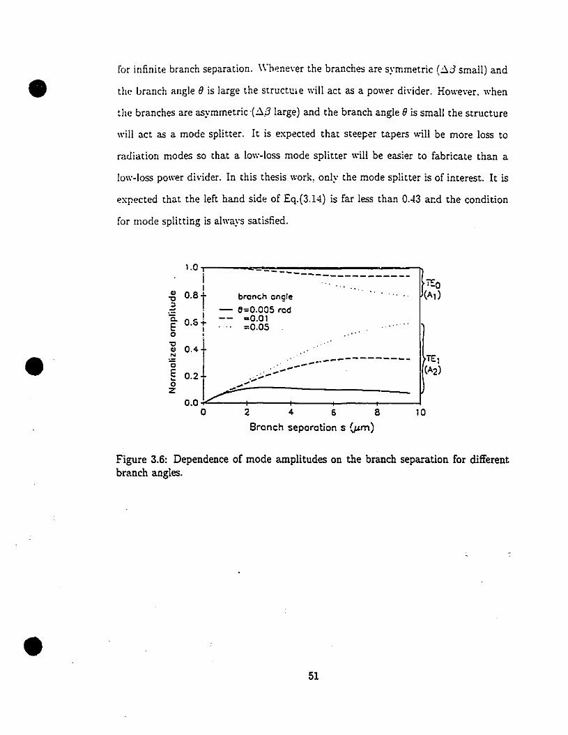
•for infinite branch separation. \\"h~never the branches are symmetric (~:3 small) and
the branch angle e is large the structule will act as a power divider. However, when
the branches are asymmetric ·(~.8 large) and the branch angle eis small the structure
will act as a mode splitter. It is expected that steeper tapers will be more 1055 to
radiation modes 50 that a low-Ioss mode splitter will be easier to fabricate than a
10w-Io55 power divider. In this thesis work, on1y the mode splitter is of interest. It is
expected that the left hand side of Eq.(3.14) is far less than 0.43 ar.d the condition
for mode splitting is always satisfied.
2 4 6 S 10
Branch separation s (p.m)
------------...;.~----_ ....
0';'"JO"..
1.011., o.St"tl.=
Ci. iE o.st0 !"tl
0.4.,N• cE 0.2~
0z
0.00
-----
bran,," angle
- Cl=O.OOS rad=0,01=0.05
--------------. " .
.' .'.. '
•
Figure 3.6: Dependence of mode amplitudes on the branch separation for differentbranch angles.
51
•
•
•
Bibliography
[1] H. Yajima. "Theory and applications of dielectrïc branching \\·a\·egllil!es··. in Proc
Symp. Optical and Acollstical ::-'licro-Elctronics. pp. 339-358. l'\cw York. ID7.J.
[2J \Y. K. Burns and A. F. ~mton. "Mode con\'ersion in planar dielectric scparating
waveguides", IEEE J. Quuntum Electon., \'01. QE-ll. pp.32-39, 1975.
[3J D. '-"Jurcuse. "Radiation loss~ of tapered dielectric siub wuveguidcs", Bell Syst.
Tech. J., vo1.49, pp.273-290, 1970.
52
•
•
•
Chapter 4
Refractive Index Measurementsand Waveguide Characterizations
Before designing and fabricating the devices, many parameters have to be
found, such as substrate indices, indices of sputtered Al20 3 layers, K+ and Ag+ ion
diffusion coefficients, and so on. Although sorne of them have been reported, there
arc still many of them unknown, especiaIly those parameters at infrared \\"avelengths
,\ = 1.31Jtm and 1.55JLm. Since the light at infrared wa\·elength is invisible, it is
more difficult to measure them than those obtained at visible wavelengths. In this
chapter, we will discuss the methods for the measurements and their accuracies.
Those parameters measured directly or indirectly will aIso be presented.
4.1 Substrate Indices
The glass substrate we used is soda-lime glass mainly due to its low cost and
its data availability in our Guided-Wave Photonics Laboratory. Its indices at infrared
wavelengths ,\ = 1.31JLm and ,\ = 1.55JLm were still not available until we measured
and established them in our laboratory.
53
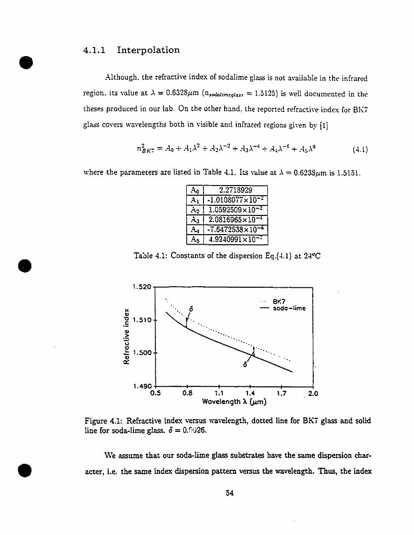
• 4.1.1 Interpolation
Although, the refractive index of sodalime glass is not available in the infrared
region, its value at ,\ = O.632Sjlm (n'odahm<9Ia,., = 1.5125) is well documented in the
theses produced in our labo On the other hand, the reported refractiw index for BKi
glass covers wa"elengths both in visible and infrared regions gi"en by [1]
(.1.1 )
where the parameters are listed in Table .1.1. lts ,"alue at ,\ = 0.623StLm is 1.5151.
•
Ao 2.2ïlS929Al -1.010S0iix 1O-~
A2 1.0592509 x 1O-~
A3 2.0S16965x 10-<.~ -i.64ï253Sx10-b
As 4.9240991 x 10-'
Ta::>le 4.1: Constants of the dispersion Eq.(.U) at 2-1°C
'. 520r----------------,
xCl>
.~ 1.510Cl>>:.:uo
.:: 1.500Cl>~
6.. BK7
- soda-lime
2.00.8 1.' 1.4 1.7Wovelength À (}.un)
1.490+---.......---+----1_--+----10.5
Figure 4.1: Refractive inde:"<: versus wavelength, dotted !ine for BKi glass and solid!ine for soda-lime glass. 6 =0.r;1j26.
•We assume that our soda-lime glass substrates have the sarne dispersion char
acter, i.e. the sarne index dispersion pattern versus the wavelength. Thus, the index
54

• n~OIfalim~ = ne;.;; - cS (4.2)
1'."1"'1"1' ri = 0.0026. Fig.4.1 shows the plots of both dispersion c\ltves. Now. we have
f1~",Jll/urlr.==1.;jOJ 1 at,\ == 1.:nJLl!1 and n,odnlime=lA98 at ,,\ = 1.5511111.
4.1.2 lVlulti-sheet Brewster angle measurement
The iudex values obtained in the last sllb-section for the infrared wavelengths
are \'Cry rough. They are guessed \'alues. It is desirable that directly measured \alues
cau be obtailled to test out the assumption made in the last sub-section.
• incidentbeam
Jens
reflections
•Figure 4.2: Reflection from a multi-sheet structure. nb is the substrate inde:", Il() isthe index of air, Fi and fi are thicknesses of the ith substrate and air gap, respectively,and m is the number of substrates. .
55
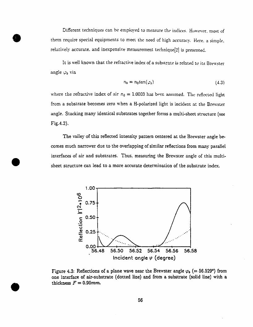
•Different technique:5 can he empioyeà to mea:5ure the indices. Hu"'e\w. most of
them require :5pecial equipment:5 to meet the need of high accuracy. Here. a simple.
relatively accurate. and inexpensiw measurement technique[2] is presemed.
It is well known that the refractive index of a sub:5tratei:5 related te) its Bre\\'ster
angle ',:b \'ia
(4,3)
where the refractive index of air no = 1.0003 has bt)el~ ,\...;,;nrned. The reflected lil;ht
from a substrate becomes zero when a H-polarized light is incident at the Bre\\'ster
angle. Stacking many identical substrates together forms a multi-sheet :5tructure (see
Fig.4.2).
•The valley of this refiected intensity pattern centered at the Brewster angle be
cornes much narrower due to the overlapping of similar refiections from many parallel
interfaces of air and substrates. Thus, measuring the Brewster angle of this rnulti
sheet structure can lead to a more accurate determination of the substrate index.
56.50 56.52 56.54 56.56 56.58
Incident ongle:p (degree)
o~oo +-~.c....--+__:..:..:..,-+>__-+~.",,~_+-__-<56.48
0.25
c 0.50o
:.:::;oQ):::Q)
0::
1.00\00- 0.75•NL
•Figure 4.3: Refiections of a plane wave near the Brewster angle yb (= 56.529°) fromone interface of air-substrate (dotted !ine) and from a substrate (so!id !ine) with athickness F = O.95mm.
56
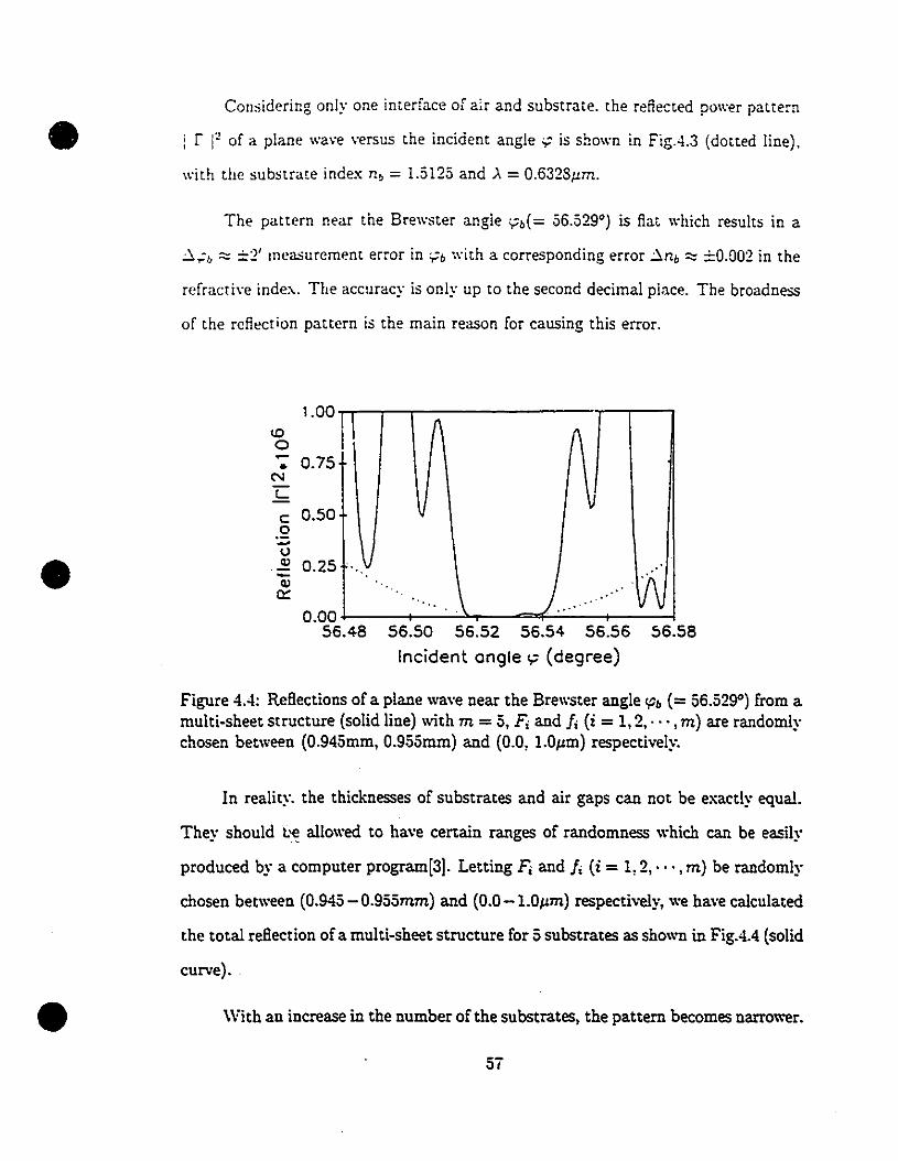
•Considering only one interface o[ air and substrate. the reilected power pattern
i r i~ of a plane wave versus the incident angle:;; is shown in Fig.4.3 (dotted line) ,
with the substrate index n, = 1.5125 and), = 0.6328Jlm.
The pattern near the Brewster angle Yb( = 56.529°) is ilat which results in a
::'.;, :::: ±2' measurement error in yb with a corresponding error ~nb ::::: ±0.002 in the
refracrive inde:\.. The accuracy is only up to the second decimal place. The broadness
of the reflection pattern is the main reason for causing this error.
1 \" fi
.,V
'ïJ\J. ... .' "" '. \ .'
0.0056.48 56.50 56.52 56.54 56.56 56.58
Incident ongle c;; (degree)
1.00<J:)
0~ 0.75•
N
L
c: 0.500
:;;.u• al 0.25ala::
Figure 4.4: Reflections of a plane wave near the Brewster angle 'Pb (= 56.529°) from amulti-sheet structure (solid line) with m =5, Fi and fi (i = 1,2,· . " m) are randomlychosen between (0.945mm, 0.955mm) and (0.0, 1.01lm) respectively.
•
In reality. the thicknesses of substrates and air gaps can not be exactly equal.
They should L'E! allowed to have certain ranges of randomness which can be easily
produced by a computer prograrn[3]. Letting Fi and fi (i = 1,2" . " m) be randoml~'
chosen between (0.945 - 0.955mm) and (0.0 -l.Ollm) respectively, we have calculated
the total reflection of a multi-sheet structure for 5 substrates as shown in Fig.4.4 (solid
curve)..
\Vith an increase in the number of the substrates, the pattern becomes narrower.
Si

• :\ comparison with the douee! curw (n'f!ection from a sin~11' itllerfan') in Fi~A.5
re\'t'als that the former is more than four times uarrower nt'ar ,'~ if 1 ::','b 1< ;?'
(f r !2< 0.13 x 10⁻⁶) for the dotted line is assumed. Thus. measurin~ .,.'b of this
20-substrate structure. one can expect the error t,o he less than DA' corresponding to
! ::'nb 1< 0.0004.
1
~\
",<o.4~".- - - F---'-- - --'. .'.',,'
1.00(0
0~
0.75..NL-
e 0.500~
uQ) 0.25-Q)
0:::
0.0056.48 56.50 56.52 56.54 56.56 56.58
Incident ongle <P (degree)•Figure 4.5: See the caption of Fig.4.4 but \\ith m=20. The dashed line indicates therange of 2' measurement error in 'Pb for one air-substrate interface.
The analysis above is based on the assumption ··ltat the incident wave is an
ideal infinite plane wave. In practice, a laser beam is used as the light source. The
total reflection of a laser beam by a multi-sheet structure contains a series of beam
spots. Fortunately, these reflected beams are all nearly parallel. They can be focused
onto one spot by an optical lens as shown in Fig.4.2. Thus, the focused spot is the
superposition of all the reflected beams and its intensity versus the incident angle
behaves just like that of the reflected waves~ under a plane wave assumption
in the previous p;;ragraphs.
•The measurement setup is very simple. A rotating stage, a focusing lens, a
laser source, and a sample holder are all that needed. For measuring the substrate
58
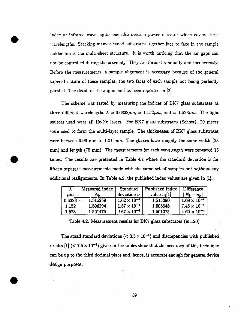
•
•
•
index at infrared waveIengths one also needs a power detector which covers these
wavelengths. Stacking many cIeaned substrates together face to face in the sampie
!loIder forms the multi-sheet structure. It is worth noticing that the air gaps can
not be controIIed during the assembly. They are formed randomly and incoherently.
Before the measurements, a sampie alignment is nccessary because of the general
tapered nature of these samples, the two faces of each sample not being perfectly
paraIIel. The detaH of the alignment has been reported in [2].
The scheme was tested by measuring the indices of BKi glass substrates at
three different wavelengths ). = 0.6328JLm, = 1.152JLm, and = 1.523JLm. The Iight
sources used were ail He-Ne lasers. For BK7 glass substrates (Schott), 20 picces
were used to form the multi-layer sample. The thicknesses of BKi glass substrates
were between 0.99 mm to 1.01 mm. The glasses have roughly the same v.idth (25
mm) and length (i5 mm). The measurements for each wavelength were repeatld 15
times. The results are presented in Table 4.1 where the standard deviation is for
fifteen separate measurements made with the same set of samples but withaut any
additianal realignments. In Table 4.2, the published index values are given in [1].
À Measured index Standard Published index DifferenceJLm Nb de"iation CT value nb[l] INb-nb!
0.6328 1.515259 1.62 x 10-' 1.515090 1.69 x 10-'1.152 1.506294 167 x 10-' 1.505548 7.46 x 10-41.523 1.501475 2:67 x 10-4 1.50101: 4.60 x 10-'
Table 4.2: Measurement results far BK7 glass substrates (m-20)
The small standard deviatians « 3.5 x 10⁻⁴) and discrepancies with published
results [1] « 7.5 x 10⁻⁴) given in the tables shaw that the accuracy af this technique
.can be up ta the third decimal place and, hence, is accurate enaugh far general device
design purposes.
59
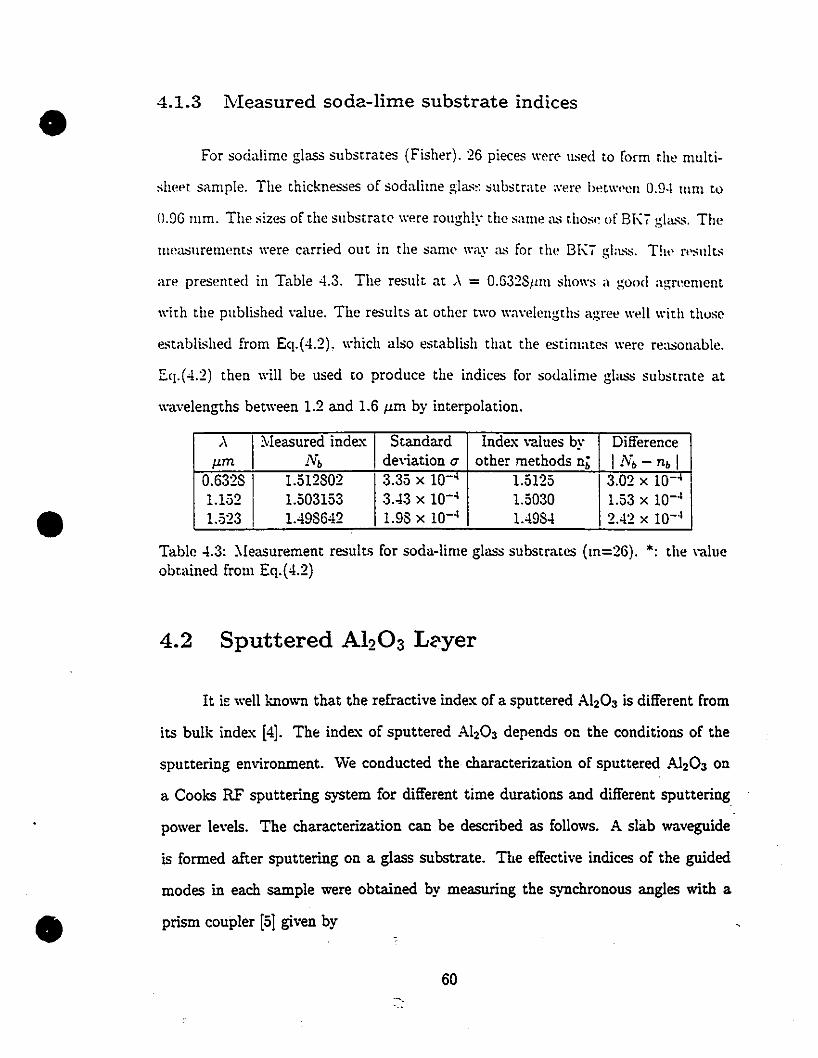
•
•
•
4.1.3 l\IIeasured soda-lime substrate indices
For ~odalime glass substrates (Fi~her). 26 pieces \\ue used to form the multi-
shep! sample. The thicknes~es of ~odalime gla.,,, ~ub~tratP ;\"ere betw,>en 0.9-1 mm to
(l.OG mm. The size~ of the substrate were roughly the saIlle as thos" of BK. glass. The
measllrement~ were carried out in the ~an\(' way as for the BK. glass. Th,' n'Sults
are presented in Table 4.3. The result at ,\ = 0.5328,tIll shows a gond agreement
with the publi~hed \·alue. The results at other two wavelength~ agree weil with t1l0se
established from Eq.(4.2), \\'hich al~o e~tablish that the estimates were reasonable.
::''1.(4.2) then \\'il! be used to produce the indices for sodalime glass sub~trate at
wavelengths between 1.2 and 1.6 tLm by interpolation.
A 1 ~Ieasured inde.'I: 1 Standard Inde.'I: values by Difference/lm Nb de\iation a other methods nb 1 Nb - nb 1
0.6328 1.512802 3.35 x 10-' 1.5125 3.02 x 10-'1.152 1.503153 3.43 x 10⁻⁴ 1.5030 1.53 x 10-.1
1.523 1 1.498642 1.98 x 10⁻⁴ 1.4984 2.42 x 10-.1
Table 4.3: )'Ieasurement results for soda-lime gl~ substrates (m=2G). *. the \'ailleobtained from Eq.(4.2)
4.2 Sputtered A1203 Lé'yer
It i5 weil knovm that the refractive index of a sputtered Ah03 is different from
its bulk inde.'I: [4]. The inde.'I: of sputtered AI20 3 depends on the conditions of the
sputtering emironment. We conducted the characterization of sputtered AI20 3 on
a Cooks RF sputtering system for different time durations and different sputtering,
power le\'e15. The characterization eau be described as fo11ows. A slàb waveguide
is formed after sputtering on a glass substrate. The effective indices of the guided
modes in each sample were obtained by measuring the synchronous angles with a
prism coupler [5] given by
60
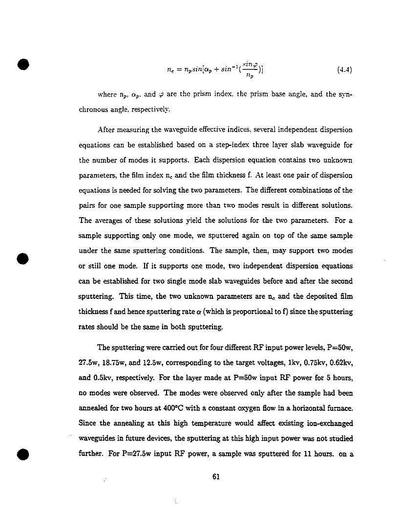
• (4.4)
•
•
where n p , op' and :p are the prism index. the prism base angle, and the syn
chronous angle, respectively.
After measurinl; the waveguide effective indices, several independent dispersion
equations can be established based on a step-index three layer slab waveguide for
the number of modes it supports. Each dispersion equation contains two unknown
parameters, the film index ne and the film thicknes5 f. At least one pair of dispersion
cquations is needed for solving the two parameters. The different combinations of the
pairs for one sample supporting more than two modes result in different solutions.
The averages of tbese solutions yield the solutions for the two parameters. For a
sample supporting only one mode, we sputtered again on top of the same sample
under the same sputtering conditions. The sample, then, may support two modes
or still one mode. If it supports one mode, two iIldependent dispersion equations
cao be established for two single mode slab waveguides before and after the second
sputtering. This time, the two unknown parameters are ne and the deposited film
thickness f and hence sputtering rate a (which is proportional to f) since the sputtering
rates should be the same in both sputtering.
The sputtering were carried out for four different RF input power leve1s, P=5OW,
2ï.5w, 18.ï5w, and 12.5w, corresponding to the target voltages, 1kv, O.75kv, O.62kv,
and O.5kv, respectively. For the layer made at P=50w input RF power for 5 hours,
no modes were observed. The modes were observed only after the sample had been
annealed for two hours at 400·C with a constant oxygen fiow in a horizontal furnace.
Since the annealing at this high temperature would affect existing ion-exchanged
waveguides in future devices, the sputtering at this high input power was not studied
furthE'.r. For P=27.5w input RF power, a sample was sputtered for 11 hours. on a
61
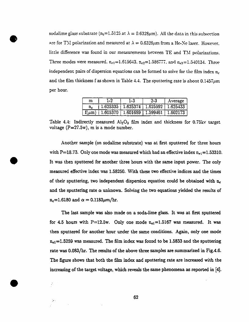
•
•
•
sodalime glass substrate (nb=1.5125 at..\ = 0.6328Ilm). Ali the data in this subsl'ction
"re for T:-'I polarization and measured at ..\ = 0.6328,'m from a He-Ne laser. Howewr.
little difference was found in our measurements between TE and T~I polarizations.
Three modes were measured. nd=1.615643. n'2=1.586ïïï. anrl nd=1.540134. Threc
independent pairs of dispersion equations can be formed to solve for the film index n,
and the film thickness f as shown in Tahle 4.4. The sputtering rate is abOlit 0.145ïllm
per hour.
m 1-2 1-3 2-3 Averagene 1.625335 1.6253ï4 1.625592 1.625433
f(l'm) 1.6053ïO 1.601689 1.599461 1.6021ï3
Table 4.4: Indirectly measured AI20 3 film inde.'I: and thickness for 0.ï5kv targetvoltage (P=2i.5w), m is a mode number.
Another sample (on sodalime substrate) was at first sputtered for three hours
with P=18.i3. Only one mode was measured which had an effective index n,1 =1.53310.
It was then sputtered for another three hours with the same input power. The only
measured effective index was 1.58250. With these two effective indices and the times
of their sputtering, two independent dispersion equation could be obtained with ne
and the sputtering rate Cl< unknown. Solving the two equations yielded the results of
ne=1.6180 and Cl< = O.ll83/lm/hr.
The last sample was also made on a soda-lime glass. It was at first sputterecl
for 4.5 hours with P=12.5w. Only one mode ncl=1.5167 was measured. It was
then sputtered for another hour under the same conditions. Again, only one mode
Oel=1.5259 was measured. The film index was found to be 1.5833 and the sputtering
rate was O.083/hr. The results of the above three samples are summarized in FigA.6.
The figure shows that both the film index and sputtering rate are increased with the
increasing of the target voltage, which reveals the same phenomena as reported in [4].
62
•~
:>o.c
0.15 ):
lSCl>
go 0.10 '0.~ ~
Cl> ~
~ 1.55 .§~ 0 ne 0.05 B... • a _~ :>o ~N ~
< 1.50+----!----+----r----+----+ 0.000.4 0.5 0.6 0.7 0.8 0.9
Target voltage V (kv)
~1.65,------------------,-0.20xCl>
".~É 1.60;:
•Figure 4.6: The dependences of AI20 3 film refractive index and its sputtering rate onthe target voltage at >. = 0.6328pm.
To obtain the refractive indices at infrared wavelengths, the dispersion of the
sputtered Ab03 film inde.'I: is assumed to be the same as that of the bulk index. For
the bulk index, we have [6]
)_ .41>.2 A2>.2 A3>.2 1/2
ne>. - (1 + >,2 _ >'r + >,2 _ >.~ + >,2 - >'5)
where those constants are given in Table 4.5.
(4.5)
>'1 =0.06144821 >'~=0.OO377588 .41=1.023798>'2=0.1106997 >.~=0.0122544 A2=1.058264x3=17.92656 >'i=321.3616 A3=5.280792
Table 4.5: Constants of the dispersion Eq.(4.5) at 24°C
•
At >. = 0.6328pm the bulk index of Ah03 given by Eq.(4.5) is 1.76596. The
cladding index at >. = 0.6328pm can be established to be 1.6254 by mode index
measurement as discussed before if the target voltage is v=0.75 kv. Thus, the film
indices of Ab03 at infrared wavelengths are approximately given by
(4.6)
63
• where ci = 1.75596 - 1.525-1 = 0.1-1056. Fig.-l.7 shows the dispersion curws for both
the bulk and cladding film of A120 3 .
1. 900r----------------,
x
"] 1. 700
">~uc.= 1.500-
"Cl::
1"' · lô ô
-'-----__--'1__
.... Al203 bulk- Al203 sputtered film
2.0
Figure 4.7: Refractive index versus wavelength, dotted !ine for the bulk of A120 3 andso!id !ine for the of Ab03 sput.tered at 0.75 kv target voltage. .5 =0.14055.
• 4.3
1.300+----+----1----1----+----40.5 0.8 1.1 1.4 1.7
Wovelength À C/Mn)
Characterization ofK+ Ion-exchanged Waveguides
•
The K+-ion diffused planar waveguide samples were fabricated by immersing
soda!ime glass substrate::. in molten KN03 at 385°C fordifferent time durations. The
waveguide effective indicés were obtained by solving Eq.(4.4) art""·. the synchronous.
angles have been measured with the prism cOllpler technique. 3ince at À = 1.152J.mi
or 1.523JLm, the He-Ne laser beam is invisible, a He-Ne laser beam at À =0.5328JLm
was used to help with the alignment as indicated in Fig.4.8 [7].
This scheme yielded an estimated accuracy of ±1.0 x 10⁻⁴ in the measur~J
effective index ne' The refractive indices of the prism coupler (Bint glass) at À =1.152JLm and 1.523JLffi were obtained from the data in [1] by interpolation to be
np=1.7523 and 1.74485 respectively. The corresponding indices for the soda-lime
substrate glass, nb = 1.5030 ± 1.0 x 10⁻⁴ and 1.4984 ± 1.0 x 10⁻⁴ respectively, were
64
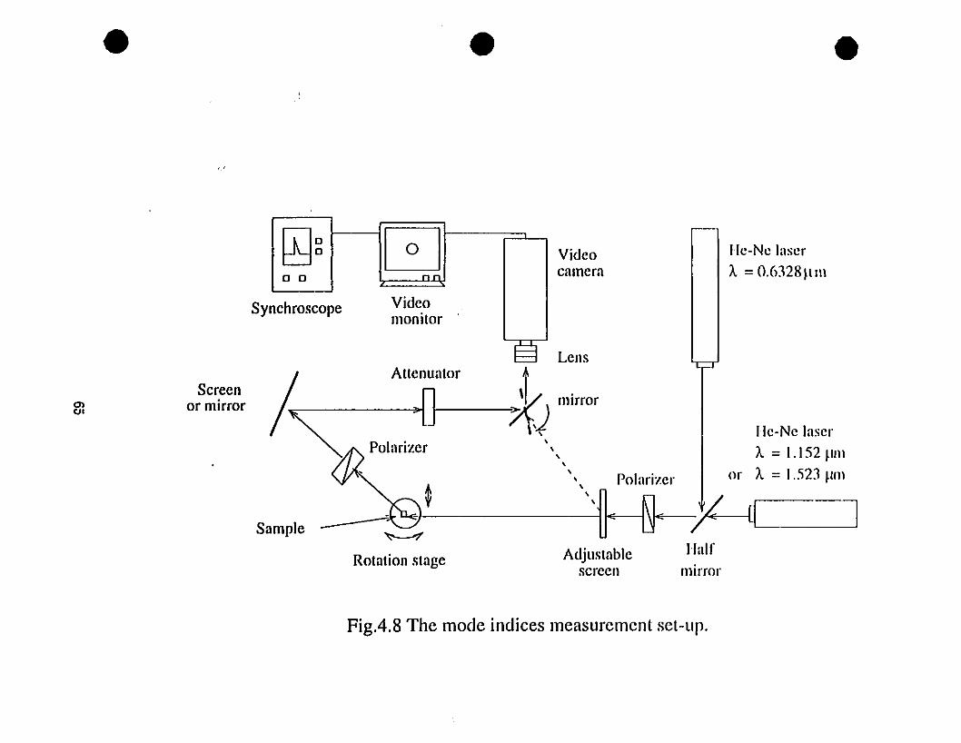
• • •
Sy
~g Go 0 nn
nehroseope Videomonitor
Videocamera
Ile-Ne laserÀ = 0.6328 ~lm
Lens
~-)L Q 1
He-Ne laserÀ = 1.152 pm
or À = 1.523 pm
HalfIllirror
Polarizer
Adjustablesereen
*~
Rotation stage
/ Attenuator t/~------"~D ~ mirror""A'- Polarizer "'" ,,,,,,
Sample
Sereenor mirror0>
<.1'
FigA.8 The mode indices measuremenl sel-ur.
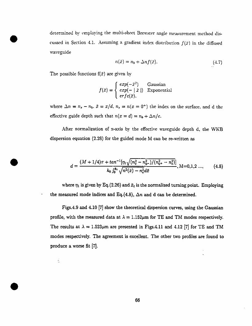
• determined by l'mploying the multi-sheet Brewster angle measurement method dis-
cussed in Section .1.1. Assuming a gradient index distribution 1(1) in the diffused
waveguide
n(x) = nb + ~nl(x).
The possible functions f(x) are given by
(.1. i)
{
exp( _x2 )
l(x) = exp( - 1 x 1)erlc(x).
GaussianExponential
where ~Tl = n.• - nb. X = x/d, Tl, = n(x = 0+) the index on the surface. and d the
effective guide depth such that n(x = d) = nb + t:>.n/e.
After normalization of x-axis by the effective waveguide depth d, the WKB
dispersion equation (2.28) for the guided mode Mean be re-written as
• (4.8)
•
where 1/1 is given by Eq.(2.26) and Xt is the normalized tuming point. Employing
the measured mode indices and Eq.(4.8), .ln and d can be determined.
FigsA.9 and 4.10 [il show the theoretical dispersion curves, using the Gaussian
profile, with the measured data at >. = 1.152~m for TE and TM modes respectively.
The results at >. = 1.523~m are pr('Sented in Figs.4.11 and 4.12 [i] for TE and TM
modes respectively. The agreement is excellent. The other two profiles are found to
produce a worse fit [il.
66
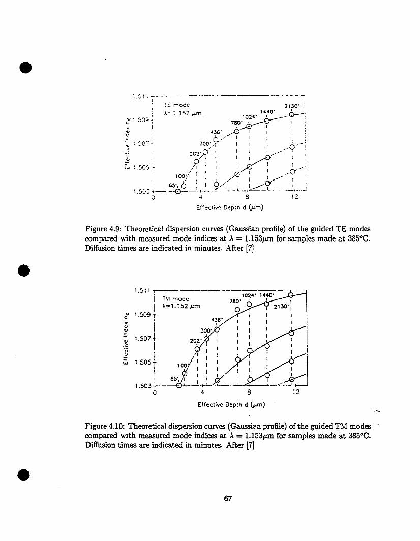
•i.511 -r--.----------
1. TE moCC
1,'=-.1.152 J.J-mc~ ~ .sO? ï• 1
'" 1U
o~
l.J 1 .~ûS ~
Effective Deplh d (}Lm)
•Figure 4.9: Theoretical dispersion cUp"es (Gaussian profile) of the guided TE modescompared with measured mode indices at >. = 1.153tLm for samples made at 385°C.Diffusion times are indi::ated in minutes. After [il
4J6'
JOO'
TM mode~=1.1S2I"m
1.511 rl---
i1
~ 1.509 T,
~ 1.s j.. 1.S07,. 202'.:: 1 1
~ 1.S0S TI ;t0o' : : 11 1 1 1
16~' 1 1 1 1 1
1.50.3 .-- ' -'.t-i- .•.- . ,o 4
Effective Oepth d (}Lm)
•Figure 4.10: Theoretical dispersion curves (Gaussilc'n profile) of the guided TM modescompared with measured mode indices at >. = 1.153tLID for samples made at 385°C.Diffusion times are indicated in minutes. After [il
6i
•1.50131"---·------ - ---'-- --- ----
,o-U
S
--121JO' ;
, 1"'0' O'102" 0- ---- -1 1
780' .J..------IiiJ.../y 1 l '
4.16' ~, , ,~ 1.~0;';, 1 ~ 1 1
~ 0 1 1 1 1~ JO?" 1 1 1 1 6 i'0' 202;0 : ,1 /---- , 1
'-J 'S00:, 9 ': :.v'~y : 1
. 100/,:, vY ' ..0-'1..;:J8.;;-- ~__ --/-.~...+--l- __ 1_ -.~I.iJ
o 4 8 12
Effective Deplh d (,.m)
•Figure 4.11: Theoretical dispersion cur\"es (Gaussian profile) of the guided TE modescompared with measured mode indices at À = 1.523/lm for samples made at 385·C.Diffusion times are indicated in minutes. After [7]
1 50G ~- --;~-m~~-e-'- ---1~2-::-~~:__~. ! ~= 1.523 ,.m 780' 2,JO' ~ 1
•.5041 '1 '1• 1 1 1 1 1" 'J6' 1~ : 1 1
~ 1.502 1 JOO' " 1
~ " 1 ~Iu 1 202' ,~ 1 1
.., 1.500
1 : 1 1 ~'1 100' 1 1 ~
14984~---- 1 l , 1 l..--- __,'
o 4 8 ,2
Effective Dcplh d (pm)
•Figure 4.12: Theoretical dispersion curves (Gaussian profile) of the guided. TM modescompared with measured mode indices at À = 1.523/lffi for sarnples made at 38S·C.Diffusion times are indicated in minutes. ACter [7]
68
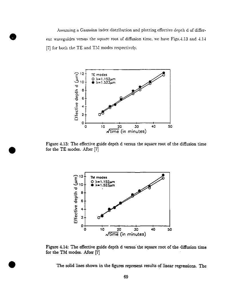
•
•
•
Assullling a Gaussian index distribution and plotting effective depth d of differ-
ent waveguides \"Crsus the square root of diffusion time. we have Figs..l.13 and -1.1-1
[il for bath the TE and T:-'! modes respectively.
-;:- 121 TE modes
2,10 1 o ,,= 1.1521"m• ,,= 1.5231"m
"J:: 8~
a.li! 6"li!>
:f:.:;uli!--w
00 10 20 30 40 50
"/time (in minutes)
Figure 4.13: The effective guide depth d versus the square root of the diffusion timefor the TE modes. After [i]
........ 12 TM modesE2: 10
0"-1.1521"""• "-1.5231"""
".r:. 8~
a.li! 6"III> 4:;:;UIII 2--W
00 10 20 30 40 50
"'time (in minutes)
Figure 4.14: The effective guide depth d versus the square root of the rliffusion timefor the TM modes. After [i]
The so\id lines shown in the figures represent results of \inear regressions. The
69
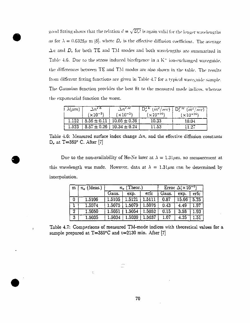
•
•
•
as for ,\ = I1.G:3281' m l8]. where D,. is r.he etf"etin' ditfusiou c'lL'tliciem. Thc av,'rage
.:la alHI D, fur both TE aatl 1'),1 1I10,ks and bath wawlt'ngths art' slllnlllarized in
Tabk -I.G. Due ra th,' stress indueed bircfrgcnCl' in a h: - i'HI-I'xl"ilang,'d waveguid,'.
r.he <lift'erenees betwCCtl TE and 1'),[ modc" arc also ,;lwwn iu 1.h., tabh'. TIlt' rl'su[rs
frolll <litferear firting funetions arc gin'n in Tabl., -1.7 fl1r a lvpil"al wa\'I'f;uid" s;,mpit-.
TIlt, Gallssian funetion pro\'ides th,' be,;t fit 1.0 tIw nW;L'llrcd 1110,1., indi,·"s. wh.'n'as
1h" ('xponehr.ial fnnetion the worse.
'\(ILm)
1
.:ln! 1:.
[
.:l/l,.I/1 0; 1:. (m~ (.,,'c) 1 of. .11 (TI!~/.,,,c) 1
(x 10-3) (x 10-3 ) 1 (xlO- lt') 1 (xIa-l") 1
1.152 1 8.56 .... 0.11 1 10.05 ± 0.36 10.33 1 10.0-11.523 1 8.5i .... 0.26 1 10.34 -l- 0.24 11.53 1 11.27
Table -l.6: ~leasllred surface index change !ln, and the eflceti\'e diffusion eonstalltsD, at 1'=385° C. After (i]
Due to the non-lwailability of He-"'e laser at A = 1.311Lm. no lllCa:;uremcnt at
r.his \\"avelength \\'US made. Howe\'cr, data ar. A = 1.31lLlll l'an hc determined by
illterpolation.
m n. (Meus.) n. (Theor.) Errol' !l( x 10-4 )
Gaus. e.'l:p. erfc Gaus. exp. erfc0 1.5106 1.5105 1.5121 1.5111 0.8i 15.66 - ?-v._v1 1.50i4 1.50i5 1.50i9 1.50i6 0,43 4.49 1.9i2 1.5050 1.5051 1.5054 1.5052 0.15 1 3.58 1.933 1.5035 1.5034 1.5039 1.503i LOi -1 ,)- 1.51._v
Table 4.i: Compllrisons of measured TM-mode indices with theoretical values for asample prepared at T=385°C and t=2130 min. After (i]
iD
• 4.4 Characterization of Ag"'" Ion-exchanged vVaveguides
()pt.ical \\'a\"egllides ha\"t~ been fabricatetl from sil\"er nitrate rnelrs dilllted \\'ith
•
•."
s"diuIII nit rat" [9]. O"pendillg 011 the tlegree of dilution. th" ''lIrfaCl' index change
,·"U 1>" adjustf'd to an" sp"cifit~d \"alue bet\\'een il and D.Da. Besitlt's. dilHrt'd silwr
i(JIl~l'xchaugp rll~crl'asC's rhe 'yellow staining" of the glass and reduc.:es th!:' \\"é1\'~311ide
l"ss...\11 thesf' Illake tht' dilutetl silwr ion-exchangetl \\'awguide a n~ry ~ol)(i candidate
in lllaking integratetl optical de\"ices. In Chapter 6. .:J.n, = 0.05 of a diluted .~g-i-
ion-exchangl'd w<lwguide is required in the wawlength demultiplexer. Based on the
results reported in [9], a \\'eight ratio of A.gN03 : ,VaN03 of approximately 1:100 is
re'luired te achie\'e this surface index change at T=325°. Although the characteriza
tion of ..ty. ion-exchanged glass waveguides at a visible wa\'elength has been reported
Ill't'\'itlllsly [9]. sirnilar work al infrared \\"1l\"clengths is not yct iwailable. Besides. a
bf'ttt'r characterization can be made with the heIp of the illlpro\'ed phase shift pre
scntl'd iu Section 2.-1 for a \\"aveguide with an index truncatiou which exists iu the
Ag+ iou-exchauged \\·a\·eguide.
4.4.1 The methodology
lt has been wide!y accepted that the inde.'I: profile of a waveguide fabricated
from a diluted silver nitrate melt can be described by a second-order polynomial [9]
giveu by
(4.9)
where do = ,jT5J is the profile depth parameter [10] and other parameters are
defined in the last section. Both the surface inde.'I: change ~n. and the effective dif-
il
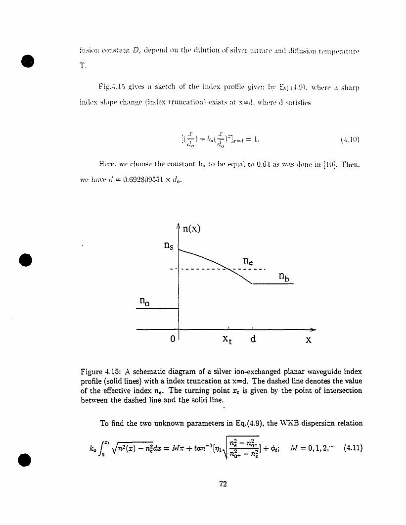
• T.
(.Ull)
•
He!"". \\",' choo,;e tht' coU,;tilnt bo w be "'lnal t,) n.G·t a,; l\'a,; ,10111' iu llil~. Tht'u.
\\"t' ha\'!' cl = 0.69:2809551 x do.
,~ n(x)
o d x
Figure 4.15: A schematic diagram of a silver ion-exchanged planar waveguide indexprofile (solid Iines) with a index truncation at x=d. The dashed line denotes the valueof the effectÎ\'e inde.'C ne' The turning point x, is gi\'en by the point of intersectionbetween the dashed line and the solid line.
To find the t\\'o unknown parameters in Eq.(4.9). the ,VKB dispersi:::n relation
•ï2
Po,[ = 0,1,2;" (4.11)
•l'ha...;" shift is gin'n in E'1.12.·IG1 with
'1 1., ., d )" .,.~ =. l"'oV'n; - nEt - I: ;"~. (~,12)
•
•
To obtain the two unknown paranll'ters. TI" and do. in a wan'gllidl'. Olt ll'a...;t tm) mod,'s
are nœded tO yield a pair of dispersion equations with dilfen'nn'>: in tilt' modf' ordl'r
:\1. These twO equations. then. can be sol\"Cd by a non-linear root 't'arch tf'chniqlll'.
4.4.2 Measurement results and discussions
The diluted salt was made of Ag;V03 1.0 : ,V'I.;\"03 100.0 in wcight ratio.
:'\ine diffused planar waveguide samples \Vere fabricated by immersing soda-lime glass
substrates in the molten salt at 325'C for dilferent time durations, 2.5. 3.0. -l.O, 5.0,
10.0, 20.0, 3.0, 40.0, and 60.0 minutes. The effective indices of the guided modes in
each sample \Vere obtained by measuring the synchronous angles \Vith a prism cOllpler.
The refractive indices of the prism coupler TIp (flint glass) at À = 0.63281lm, 1.152Ilm,
and 1.5231lm are 1.ïï862, 1.ï5231, and 1.ï4486, respectively. The corresponding
indices for the substrate glass nb are 1.5125, 1.5030, and 1.4984 respectively.
Fig.4.16 [11] shows the surface index change versus the diffusion time for TE
modes at À = 0.6328Ilm. The independence of t.n. on diffusion time can be clearly
seen. Similar results are also true at other "..avelengths for both polarizations. We
took averages of n. among the samples (multi-mode) for different wavelengths and
polarizations as listed in Table 4.8 [11].
According to the calibrated results in [9] at À = O.6238llm, the surface index
change isO.05 which is very close to our results. The results in Table 4.8 also show
ï3

•Ulod,o samplcs.
0.04
0.08
10.06
À=O.6328(,um). TE mode
Cl0'Co.r:uxIII
"0C
IIIU~ 0.02'::>
(/)
00 o o o o
7525 50
Diffusion time (min)
0.00-!------+-------+-------lo
Figure 4.16: The surface index change dependence on the diffusion time for TE modesat >. =0.6328JLm at 325°C.•
>'(JLm) 0.6328 1.152 1.523TE 0.049 0.048 0.046TM 0.049 0.048 0.048
Table 4.8: Measured average surface inde.'I: changes at 325°C
\Vith n. known, we can obtain the dispersion curves for different modes by the
modified WKB method. Plotting the measured effective indices together with the
dispersion curves, we ha~"e Figs.4.1ï, 4.18, and 4.19 [11] as illustrations.
Fig.4.1ï show that the results obtained by either \\'KB or M\VKB are ~"ery
close in multi-mode regions. But near cutoffs, the measured results are closer to the
•cun-es obtained by MWKB. Figs.4.18 and 4.19 have been enlarged in comparison
with Fig.4.lï for a cloSer look at the single mode regions. The cun'es obtained by
M\VKB obviously pro~;de a much better fitting.
ï4
• Fig~ ..L~n and ~1.:21 :r 1: indicatt' the rdatilHl h~,t\\"t't'l1 tht' nnrmali/t'd W;\\'{',.:.uidt'
dl'llth a!H! tilt' ,quan' rUll! ,)f rlH' ditfu,iuu riml'. Tht·y art' liIH'arly dt'IH'!Hlt'nr :L'
t'Xpt'l'tl'cl. TIlt' ,lup~, of rhl' bl"! tint'd lint" f<lr IHllh rht' TE and T~l pularizari'ln,
ar rlH' rhn'l' wa\"l'lPngrh, aft' gh·t'n in Ta!>lt' ~.9. \\'t' l'an ,t't' al,u in Fig, ..l.~ll and
..L:?l that tht' titting linl~~ alnh):-;t pa.....s thrtHlgh tht' {lri~in. Sitllilar rt':-;Illt~ art' abtl
!rUt' in other \\'a·.·el~ngth,. Tht' ft',ulr, in Ta!>!l' ·1.9 an' al'('lIrarl' r<l rht' tir,! dl'l'ima!
plan' and yi~ld approximatt'iy 1.5..-\cl'ording to n',ult, pn"t'ntl'd in [9] ,/15;. = I.;-,S
(J1m/v'rnin). Our \'alu~ ar~ ,lightly smaller.
,\(J17n) 1 0.6328 1 1.152 1.523TE mode : 1.49; 1 1A50 1A94T:\! mode 1 1.531 1 1A80 1.509
Table 4.9: :\!easured square root of diffusion coefficients (JnnNmin).
),= 1.152(,um), TM mode1.550,-------------------,
1.525(1)
>.....(.)
2 1.514-W
60'140'
... WKB- MWKBo Meosured1.538
(1)
C
x(1)
'0C
•
15:3 5 9 12
Profile depth pOïometer do(}Lm)
1. 502 +--...:.....-+-----=--+-----'-+--~--~o
Figure 4.1 ï: Theoretical dispersion curves, - MWKB and ..... WKB, of guided TMmodes are compared \\ith measured mode indices at .À = 1.152Jlm for samples madefar different time duratians (in minute) at 325°C.
•ï5
6---4
2
' .... --.. ~:::
5: .3 - 0 ~.'ess'_'sc
. . 5'-- 'I~-:.:-"; '. ~..)U'~""":""'" 1:' i:""'.::-:e
i. 5 ~ ê --- --------- .--------------. --;r-/"'..... ,/'
'c /"'/
~
Y,.o,
4' .
1,. f).
? 5' ~ /~.
-?:P ./
,!11
1. 498 -'-:-------!----'----~û
<:J i. 508 -:>~
U<il 1. 5û.3 ~~
~
w
•
Profile depth pcrameter doCum)
•Figure 4.18: Thcoretical dispersion curves, - :'.1\\1":8 and ..... \\"K8, of guides modesarc compared with measured mode indices at ,\ = 1.523/Lm for TE modes for singlemode samples at 3:25°C.
t-=' .523(,um), TM mode1.518-r------------------:;~
1.508Qi>....(JQi , .50.3..........
LU
<llC
xQi
<:JC
1.51.3
WKB- MWKBo meosured
la'
62 4
Profile depth parameter do(.u.m)
1.498+-----_--"-----+-----~o
Figure 4.19: See the caption of FigA.18 but for TM modes.
•ï6
• \=O.ê.325 !J.rn. ï~~ :--: ç C '2~
'5 ~-----~
~ , 1 .'~-':5' 1
! --, i
" 10 l/--'
1
" v/ 1~
c:
ç;/1
0'-0c...=:
511- ,
C- I""'0
1"-01'- O. 1C- o 2 4 6 8 la
Jt(min)
Figure -1.20: Index profile depth parameter wrsus square root of ditfusion ti~ne at,\ = 0.632Sf'm for T~l modes.
À= 1.1 52(JoLm). TE mode• '""' 1S
iE:l
"='if''-III
la l-IIIE
,0 1'-0
,1a.-'=-a.III
"III-0'- ac- o 2 4 6 8 la
..)T(min)
Figure 4.21: Index profile depth parameter \'ersus square root of diffusion time at,\ = 1.152f'm for TE modes,
•TI
•
•
•
Bibliography
'1 ()/J!/nl! .\falt'ru:l.'i. Upric~ Gllidt'·1 (~dellt.~ GritJt (\lt"puratil):l. Ir\"it~!'. CaUf. IDSSL
pp.:;-II!.
[:!; F. :\:an.~ amI G.L. Yip. "Simple techniqne for dt,terminiIl!; substrate indices of
isotropie m,lterials oy a multisheet Brewster aIlgle measurement". Applied Op
tics. vol. 31. ;';0. 36. pp.75ïO-ï57-l. December 1992.
[:3] \\".H. Press. B.P. Flannery. S..-\. Tenkolsky. and \\·.T. \·etterling. .Yumerical
R.,ôl"·s (Cambridge l·. Press. :'\e\\" York. 1986). Chap. 7. pp.191-2:25.
[-li C.W. Pitt. "Sputtering-glass optical \\"aveguides". Electron. Leu.. \'01.9, N'o. 1ï,
pp.-101--l03. 19ï3.
[5] P.K. Tien and R. Ulrich, "TheOI'y of prism-film coupler and thin-film light
guides", J. of the Opt. Soc. Am., vo1.60, No.10, pp.1325-l33ï, 19ïO.
[6] I.H. Malirson, "Refraction and dispersion of synthetic sapphire", J. of the Opt.
Soc. of Am., vo1.52, p.13ïï-13ï9, 1962.
[7] G.L. Yip, K. Kishioka, F. Xiang, and J.Y. Chen, "Characterization of planar
optical \\"aveguides by K+-ion c-'l:change in glass at 1.152 and 1.523 J.Lm", SPIE
Proceedings, vo1.1583, pp.14-l8, 1991.
[S] G.L. Yip and J. Albert, "Characterization of planar optical waveguides by K+-ion
exchange in glass", Opt. Letters, vol. 101, pp.15l-l53, March 1985.
ï8
• , ,
•
•
in ti", n!'ar infrarcd··. SPIE rr0l'l·t·dill~S. \'01.170·1. 1'1' ..111.-17. lù~" .
ï9
•Chapter 5
An Al20 3 Strip Loaded Y-branchWDM for À = 1.55 and 1.31f.Lm byK+-Na-: Ion-exchange in Glass
5.1 Introduction
• TIll' objecti\'e of this work is to design and fabricate a Y-junction \\"D:-'1 for
.\=1.31 and 1.551LnI as shown in Fig.5.1. Its wawguides ar(: made by K~ ion-exchange
with its arm :2 cladded by an Al20 3 layer. The demuitiplexing is based on mode trans
formation from the fundamental mode in the input wa\'eguide to the local fundamental
mode of the 5-layer branch structure and the difference in the dispersion character
istics of the two dissimilar branches. For efficient demultiple:cing, a large difference
between the effective indices of the two branches is desirable based on the conclusions
drawn in Chapter 3. It can be achieved by a waveguide asymmetry, consisting of
two branches \\;th a different height and \\;dth. The e.'l:tinction ratio (ER), defined
by the ratio of both the fundamental modal powers from the two infinitely separated
branches, can be further enhanced by an Ah03 layer over one branch (branch 2).
•The design was first proposed in [1]. However, it is far from being optimized and
little progress has been made to achieve reasonable e.'l:tinetion ratios e.'l:PerimentalIy
so
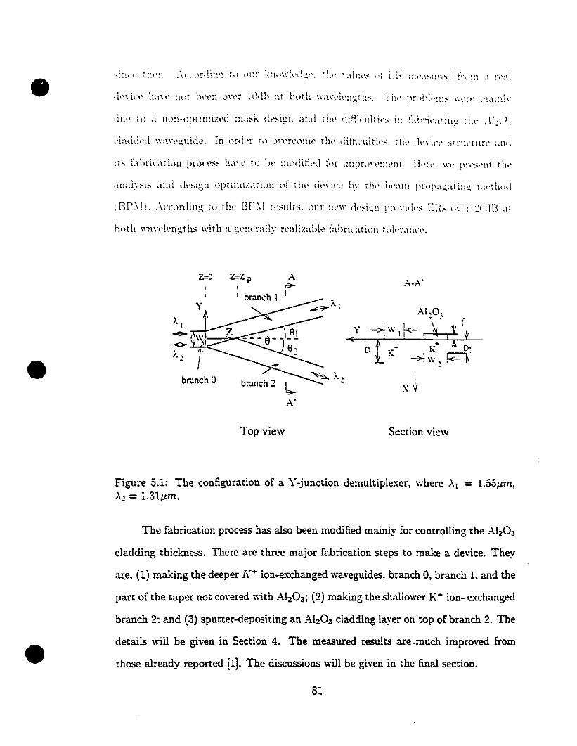
•
hoth \\"a\"(~l..'ngths with a gt'ut'rally l"l'alizablt' fabricati~>tl r~II,·ralll·t·.
z=o z=Z p AA-A'
~
1 branch 1 1
Y AI,O.
". 't - .' f~w k- \,
~~Z y
1 Il-.' 0 ,
• • D-i.. ., l' DI K K
1 ~~r1~w.,• branch 0
X~branch 2
Top view Section view
•
Figure 5.1: The configuration of a Y-junction demultiplexcr, where À l - l.55J.lm,À2 = ~.31J.lm.
The fabrication process has also been modified mainly for controlling the Ah03
cladding thickness. There are three major fabrication steps to make a device. They
;u:e. (1) making the deeper K+ ion-exchanged waveguides, branch 0, branch 1, and the
part of the taper not covered with A120 3 ; (2) making the shallower K" ion- exchanged
branch 2: and (3) sputter-depositing an Al20 3 cladding layer on top of branch 2. The
details will be given in Section 4. The measured results are.much improved from
those already reported [1]. The discussions will be given in the final section.
81
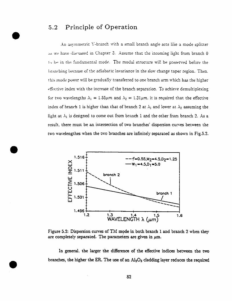
•Principle of Operation
AIl asyrnrnetric Y·branch with a small branch angle acts like a mode splitter
;c' '."" have discllsseè in Chapter 3. .-\.ssume that the incoming light îrom branch ar" b.' in tiF' fllnda:nental mod('. The modai structure will be preserwd before the
i,ranching because of the adiabatic invariance in the slow change taper region. Then.
rhis mode power will be gr2dually transferred to one brandI arm which has the higher
..ff,·ctive index with the increase of the branch separation. To achieve demultiplexing
for t\\·o wavelengths '\1 = 1.551,m and '\2 = 1.31pm. it is retjuired that the effective
•
index of branch 1 is higher than that of branch 2 at '\1 and iower at '\2 assuming the
light at '\1 is designed to come out from branch 1 and the other from branch 2. .-\.S a
result, there must be an intersection of two branches' dispersion cun'es between the
two wa\'elengthes when the two branches are infinitely separated as shown in Fig.5.2.
--f=0.55.W2-4.5•02=1.25-W1 -4.5.0, -5.0
1.516xwaz 1.511
:-........ branch 2
~ .........................J1- 1.506 _() ---- ..............w --------=::....::....:::::::::...__::::::::::~~:~_u.. ........ branch 1b 1.501 -............ /
----- -----, .6
1.496+-----+-----+-----+------l1.2 , .3 , .4 1.5
WAVELENGTH À (u.m)
Figure 5.2: Dispersion curves of TM m<;lde in both branch 1 and branch 2 when theyare completely separated. The parameters are given in pm.
•In generai, the larger the difference of the effective indices between the t\vo
branches, the higher the ER. The use of an AI20 3 c1adding layer reduces the required
82
•; ",,:, l' l '" '1 .j,') D ..,;:..... , "1 ••'.' ' •.• ~, , .. -,.,., ,.".: '" '\ 1 1'.' :01 •• " ,\,.l .. t .. _..> .\ ..1•.• ' •• ll ••. l.~.l.... t:-- ' •• t .\:--\ ..... It .• : ,lt',,\t',-:: \ H' l\YI\ Ir:t!\l',lI':-,
d"Ilt'ndt'm tHl rhl' brandI <lng1t' li. If li js nor small t'nollgh. rht' brandi will ;\<.( as a
ptl\n'r diyider insteaù of a mode splittt'r. The limit of li i:i gin'n in E'I.I:U.\). ln tht'
f,)lIowing. we a....;sume r.hat all the branch angles li satlsfy Eq.(3.1 ..n. The indices of
:\I~03 sputtering layer are giYen in Table ·t-l after the targ,"t mItage of the spllttering
'-'"cre set ta 0.75 b·.
• 5.3 BPM Analysis and Design Optimization
The etfeetlye index method has been used ta simplify the de\'iee from a three..
•
,Iimensional problem to a two-dimensional problem before the BP~l is use,L For the
wayeguides made by the first K'" ion..exchange, the \-\iKB dispersion equation (2.28)
is used to calculate n~" of the slab wa"eguide (ô/ôy = 0) with Dl as the waveguide
depth. The inde..'I: profile of this slab waveguide is assumed to be Gaussian as diseusscd
in Chapter 4. For the AhOJ c1added waveguide, the dispersion equation (2.36) will
be used to find n:". Again, the K+ ion..e..'l:changed shallow waveguide index profile
is Gaussian. Then, the deviee ean be approximated ily a slab-branch structure as
show'n in Fig.3.1 where all the equivalent indices are wavelength dependent and all
the index dependence along y are assumed to be step-like.
The BPM can, now, be applied to solve this two-dimensional problem. Tremen..
dous computing time tan be saved in the BPM simulation employing a two-dimensional
83
(5.1)
•
•
furtllulat.iun insU'ad of a thn·(··dirnt.·nsional one. On t.he other hand. the on!y large
ind,'x di,C"Ontinuit.y apP,'ars un the waveguide surface. Thb discontinuity l'an be eas-
ily consider<'d in the \\'I-:B Illethod sueh that a structure wit.h a \'t'ry smail index
challge is left for analysis by the BP:'-.1. This is especially good when a wctor BP:'-.!
W'L' not yet a"ailable. For this historie reason. only the FTT-BP:'-.! were used and
will be presented in this chapter. The BP:'-.! window was 100!-,m wide. the transwrse
grid size was 100/512 Ilm. and the propagation step size was 2!-,m. The fundamental
eigenfunction was input al. z=O as shown in Fig.5.!. The output powers (fundamental
modes only) from two branches are calculated al. where the separation is sufficient
large, for example 20!-,m.
The extinction ratios were calculated by using the following definition
ER _ { 10/ogto (~) for "t- 10/ogI0 (f;7) for "2
where p\ and P2 are the powers of the fundamental mode in branch 1 and branch
2 respectively. In the calculations, all the media were assumed 1.0 be lossless. The
power from its designed branch in the fundamental mode is considered as the received
power, i.e. Pl or P2 • The other power is taken as loss, which includes the reflected
power, the scattered power, the power going into another branch, and the power
carried by higher-order modes. Here, we cali this loss a de\'Ïce loss, which l'an be
expressed by
{lO/oglO( Po;"P. )
de\'Ïce loss = 10/og\0(&;."')
where Po is the input power.
5.3.1 ER dependence on the branch angle
(5.2)
•Although, in Chapter 3, il. has been demonstrated that the performance of a
mode splitter strongly depends on its branch angle, a detailed anal~ of ER with
respect to the branch angle by the BPM for a Y-branch is still necessary.
84
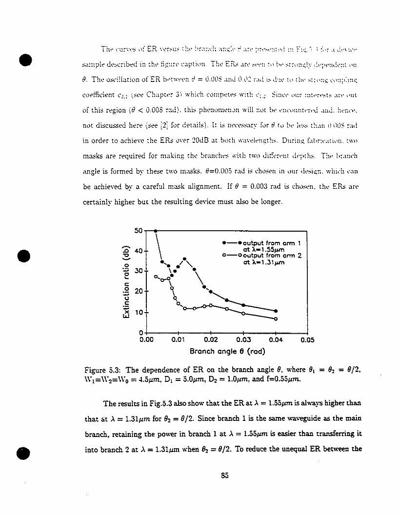
•not discusseà h~re (see ~21 fùr dNails). l~, is nt'l"t',Ssary fùr 8 t0 bl' lt l :-;:-; t~~a!l II \)ùS rad
in order to achiev(' the ERs ù\"er ~OdB at b~)th \\·a\"dt·!l~ths. Dl1riIl~ Llbr~ran~)n. tWll. .
ffia$ks are requireà for nlaking tht.:' branches ~\'ith t\\'o Jitfl'rt'IH dt,tlt hs. Tilt' brandl. .
angle is formed by these two masks. 8=0.005 rad is chost'n in our tit'si,,::. Will":' t'an
be achiewd by a careful mask alignment. If B = 0.003 rad is chost'n. the ER,; are
certainl:;- higher but the resulting de\'ice must also be longer.
• -.D 40't:l.......o
:;:; 30o'-c:~ 20
<.1c:
:;:;x la
t.J
e-eoutput Irom orrn 1at >'-1.55jUTl
o-ooutput lrom orrn 2at >'-1 .31 jUTl
0.05
•
O+---+---I-----+-----l~-_l0.00 0.01 0.02 0.03 0.04
Branch ongle Il (rad)
Figure 5.3: The dependence of ER on the branch angle 8. where 8, = 8z = 8/2.\V1=\\"z=\VO = 4.5~m, D, = 5.0~m, Oz = l.OJLm, and f=O.55~m.
The results in Fig.5.3 also show that the ER at >. = 1.55JLm is alwa:'S higher than
that ât >. = 1.31~m for 8z = 8/2. Since branch l is the same wa\'eguide as the main
branch, retaining the power in branch l at >. = 1.55JLm is easier than transferring it
into branch 2 at >. =1.31JLm when 8z =8/2. Ta reduce the unequal ER between the
85
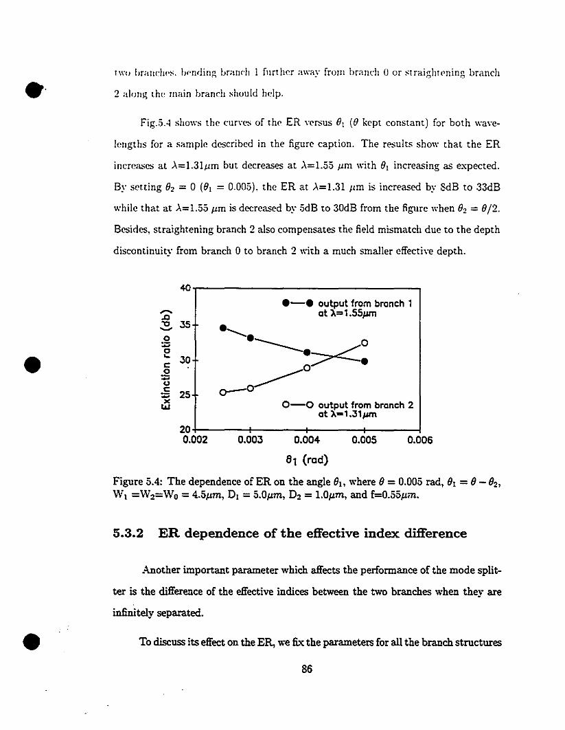
e·Iwo brandll's. IJf'nr!ing brand, 1 fllrth~r away from brandI 0 or srraight~ning brand,
2 along the main brand, should help.
Fig.5A shows the cur\'es of th~ ER versus BI (B kept constant) for bath wa\'C
lengths for a sampl~ described in the figure caption. The results show that the ER
illcreases al À=1.31/lm but decreases at À=1.55 /lm with BI increasing as expected.
By setting Bz = 0 (BI = 0.005), the ER at À=1.31 Jlm is increased by 8dB to 33dB
while that at À=1.55 /lm is decreased by 5dB to 30dB from the figure when Bz = B/2.
Besides, slraightening branch 2 also compensates the field mismatch due to the depth
discontinuity from branch 0 to branch 2 with a much smaller e!fecti"e depth.
4Or----------------,
•.......c~ 35o
:;;;ec: 30o
:;;;(,)
;; 25x~
.-. output trom bronch 1at À=1.55Jml
0-0 output trom branch 2at >'-1.31Jml
0.0060.0050.00320-l-----1------t-----t----l0.002
Figure 5.4: The dependence of ER on the angle Ih, where 6 =0.005 rad, 61 = 6 - 62,
WI ='W2=WO = 4.5JLm, DI = 5.0JLm, D2 = l.OJLm, and f'-0.55JLm.
5.3.2 ER dependence of the effective index difference
•Another important parameter which affects the performance of the mode split
ter is the difference of the effective indices between the two branches when they are
infinitely separated.
To discuss its effect on the ER, we fix the parameters for aU the branch structures
86
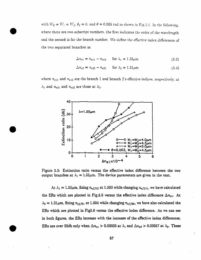
•with ll"o = ll"l = Ir". e" = O. anà e=0.005 raà ;L" "hl)\\"!1 in Fip:.5.1. ln th.' f"l1l)wing.
where there are two subscript numbers. the first indicates th., ordl'r of the wa\'d,'ngth
and the seconà is for the branch numbcr. \\'c definc th.' eF.eetiw index ditferences of
the two separateà branches as
for .\~ = 1.31/Ll1l
(5.3)
(5..1)
........0~30
o:::ec 20o
:::CJc
::: '0xW
•
•
where ndl and nd~ are the branch 1 and branch 2's etfecti\'e indic.,s. respecti\·dy. at
'\1 and n.~l anà n.22 are those at ,,~.
40,-----------=--....,.... ..,
a-a W, =W2=4.0~0-0 W, =W2=4.5~6-6 W, =W2=5.0~
.-. 6=0.003. W, ""W2=4.5~O+----+---+--~I__--+-=---=+--=-___l
0' 23456ânelXl0-4
Figure 5.5: Extinction ratio \'ersus the effective index difference between the twooutput branches at "1 =1.55JLm. The de\'ice parameters are given in the text.
At "1 =1.55JLm, fixing n.!f12 at 1.500 while changing n.!fll. we have calculated
the ERs which are plotted in Fig.5.5 versus the effective index difference .!ln.l' At
"2 = 1.31JLm, fixing n.//21 at 1.504 while changing n./f22. we have also calculated the
ERs which are plotted in Fig5.6 versus the effective index difference. As we can see
in both figures, the ERs increase with the increase of the effective index differences.
ERs are over 20db only when .!lnel > 0.00033 at "1 and .!ln.2 > 0.0005i at ).2. These
Si
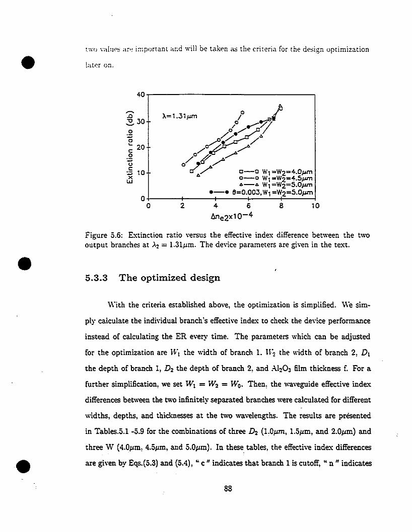
•
•
•
(wC) vallJP'; aror important and will be taken as the criteria for the design optimization
!a.tcr on.
40.,...----------------...,,......0~30
o:;:;o... 20co
:;:;
"c:;:; '0x
W
Figure 5.6: Extinction ratio versus the effective index difference between the twooutput branches at '\2 = 1.31JLm. The device parameters are given in the text.
5.3.3 The optimized design
\-Vith the criteria established above, the optimization is simplified. We sim
ply ca\culate the individual branch'5 effective inde:" to check the device performance
instead of calculating the ER every time. The parameters which can be adjusted
for the optimization are !-rI the width of branch 1. tr2 the width of branch 2, Dl
the depth of branch l, D2 the depth of branch 2, and Al~03 film thickness f. For a
further simplification, we set Wl = W2 = Wo• Then, the waveguide effective inde."<
differences between the two infinitely separated branches were calculated for different
widths, depths, and thicknesses at the two wavelengths. The results are prësented
in Tables.5.1 -5.9 for the combinations of three D2 (1.0JLm, 1.5JLm, and 2.0J.'m) and
three W (4.0JLm, 4.5JLffi, and 5.0J.'m). In these tables, the effective inde."< differences
are given by Eqs.(5.3) and (5.4), "c Il indicates that branch l is cutoff, "n Il indicates
88
•
•
•
rhar rlw t'rft'crin' dif'ft'l"{'!lCt' a:-; dt'tinl'd h\· Eq:'.(.-).:31 and \.-L·I~ i:-; 11t'~atl\'t'. ;\lld tlll'
dOllbll' liHl':-; mark rh..'" bÙllndaries L)\"t'r which hrandt :2 will ~I1PPl\rt a ~1'('()IHI-llrdl'r
1110dl.' at ~\"2 with a fl1rther incre~~e in f. .-\.lthùllgh t.ht' :,idl'-llitfl1~illn ur it1l\-t'xchallp,t'
tlIa~' Ilot bt' ÏIllpùrr.ant in thè ùesign. it can not lH' c()tllph'h'l~' i~tll)n'tl. lt i:-: hard
r" ma!;,' a det'p wa\"(~~uid,'. for "l'ampk Dl = li.lIIHU. \\"ith a !laIT"\\" \\"!<lth ,,l' rlH'
tuas!; Will,l,)\\·. for "l'ampl,' Il;, = -l.lIllIIl. b\' I>ltrt'I\' th"rlual j"t ... ·x ..hatl".!,'·. Il''1''' lt j,
assumetl t'lat DI :S II'" .;- l.Üllm.
Thus. "'C' inùicare the enclosed regl')l\S m highlight ill th,' tahlt·s thar j>1,·",·tlt
thl' designs hm'ing the ERs ('ver 2üdb for bath the \\'awlengths an,l satisfvin~ tht'
conùitions mentioned abo\·e. The tables sho\\' that the ERs arc \'Cry Sl'nsiti\"l~ ta the
Al20 3 film thickness f. To pro\'ide the ERs over 20db. l' has ta be accurate up to
about O.OI/LIll which is very difficult ta COntrol. COIllpared with al! the sizes of th"
t'ucloseù regions in the tables, the areas in Tables .5.2 and 5.5 are the two biges!.. If the
parameters of the de\'ice are chosen from the middle of the two endost'd rt'gi'llls. tht'
design shouid be close to the optimizeù one. In these regions, the parameters pro\'ide
the largest fabrication tolerance for the ERs over 20db at both the \\'avelengths.
But its ERs are not necessarily the highest ones. This near-optimized design is
Dl = 5.0 ± 0.5fLm, lVo = HOt = ni:z = 4.5 ± 0.5fLm, D 2 = 1.25 ± 0.25fLm. and
f = 0.55 ± O.OlfLm.
89
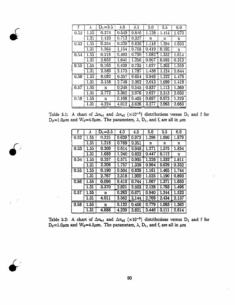
••
f 1 À 0,-3.5 [ M'I 4.5 1 5.0 1 5.5 1 6.0i O.5:! 1.55 0.2i4 0.549 0.8J6 1 1.138 lA14 1 1.6iO1 1.31 1 1.123 0.i13 0.32i n
1 n 1 n0..53 1.5.) 0.254 0.529 0.826 I.US 1 1.394 1 1.650
1.31 1.564 1.154 1 O. i68 0.419 1 0.105 1 n0.54 1.55 1 0.218 0,493 1 O. i90 1.082 1.352 1 1.614
1.31 1 2.0.52 1.641 1 1.256 0.90i 0.593 0.3130.55 1.55 0.163 0.438 0.i35 1.02i 1.303 1.559
1.31 2.583 2.li3 l.ï8i 1.438 1.124 1 0.8440.56 1.55 0.082 0.35i 0.654 0.946 1.222 1.4i8
1.31 3.158 2.i48 2.362 2.013 1..699 1 1.4190.5i r..55 n 0.248 0.545 0.83i 1.113 1.369
1.31 3.in 3.362 2.9i6 2.62i 2.313 2.0330.;i8 1.55 n 0.108 0.405 0.69i 0.9i3 1.229
1.31 4.224 4.012 3.626 3.2ii 2.963 2.683
Table 5.1: A chart of ~nel and ~ne2 (x 10-3 ) distributions versus DI and f for02=1.0pm and Wo=4.0pm. The parameters, À, Db and f, are ail in pm
f À 0 1-3.5 4.0 4.5 5.0 5.5 6.00.52 1.55 0.325 0.639 0.9i3 1.296 1.600 1.8i9
1.31 1.218 0.769 0.351 n n n0.53 1.55 0.300 0.614 0.948i 1.2il 1.575 1.854
1.31 1.689 1.240 0.822· 0.447 0.112 n0.54 1.55 0.257 ü.5il 0.905 '1.228' 1.532" . 1.811
1.31 2.206 ·1.757 1.339 0.964 0.629 0.3320.55 1.55 0.190 . 0.504 0.838 1.161 1.465 l.i44
1.31 2.767 2.318 1.900 1.525 1.190. 0.8930.56 1.55 0.096 Q.410 0.744 1.067 1.3i1. 1.650
1.31 3.370 2.921 2.503 2.128 1.i93 1.4960.57 1.55 n 0.283 ;0.6i1 0.940 1.244 1.523
1.31 4.011 3.562 •3.144 2.769 2.434 2.137
0.58 1.55 n 0.122 0.456 0.779 1.083 1.3621.31 4.688 4.239 3.821 3.446 3.111 2.814
Table 5.2: A chartof .!lnel and ~ne2 (xl0-3) distributions versus DI and f for02=1.0pm and Wo=4.5JL11l. The parameters, À, Db and f, are ail in pm
90
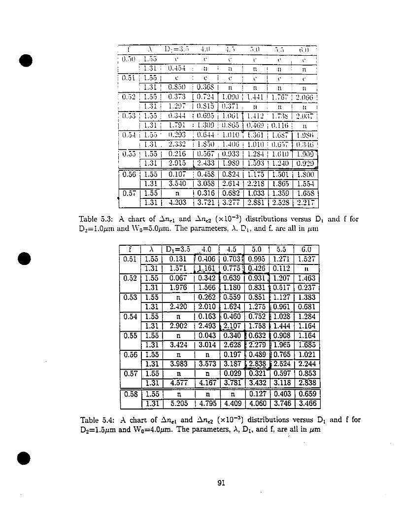
Ül ' - ,-, ,Il li ,1 J" , .l,.)
(' l' l'
"l'
li li t: li li
C (' (' (' ('c
O.S~,O : 0.:3GS 1 li li i li li
; 0.51 i 1.55 i1 1 1.:31 :
f .\ D· -:'> ..-)• ll. ,-'1) I.~;) l'i
Ul IU5-l
[ D.';2 [ 1..';5 !1 l ., l '1 •• ) ~
0.:37:3 1 D. ,2·[ 1.0911: U·ll 1 1. ïGï ! 2.0GG '1.29ï 1 11.815 IUïl, li 1 li 1 li
iJ.:3-l-l 10.G9;) 1 I.11Gl U12 1 l.ï:3~ 12.U:;ï 1l.ï91 : U09 [ U.8G5 Ill.-IG!J i IJ.llli i li 1
1l.293 [ll.G-I-i 1 LOlO , t.:lGl 1 l.G8ï l.981; 1
2.:3:32 i 1.851) 1 l.·lillj , ltlll) : 1) Go,ï 10 :;.IL> 1,
ru·531
1.55 1 O.21G 1 D.5G7 i 11.93:3 : 1.28·[ 1 1.l; 1Il 1 l.!JO!J1 1.31 1 2.915 l 2.-133 1.989 1 1.593 l.2-lD 1 0.929,
0.5G 1.551 0.107 : 0.-158 0.82-l 1 1.1ï5 1.501 1 1.S0D
1 1.:31 1 3.5-10 1 3.058 1 2.Gl-l 1 2.218 1 l.8G.'; 1.5.';-l0.57 1.5.5 ! n 1 0.316 1 0.682 1 1.033 ! 1.359 1.G58
1.31 1 -l.203 i 3.721 3 ·r- 1 .) 881 1 .) "')8 1 .) "1-._1 j _. _.v_ _._ l
i O.;)-l 1 [.;);) 1
1 1 I:H
: 0.:;:3 : 1.:;5 '1 i Ul 1
•Table 5.3: A chart of ~nd and .:ln.2 (x 10-3 ) distributiolls \'crsus DI and l' for02=1.0tLm and \Vo=5.0ILm. The parameters, ,\. Dl, and f. are ail in ILlll
f 1 A 1 0 1-3.5 '.4.0 1 -1.5 5.0 1 5.5 1 G.O 1
0.51 1.55 0.131 0.-106 O.'03~ 0.995 1.271 1 -.)-.'>_1
1 1.31 1 1.571 Jcl6:l 0.••5 ' Q.-I2G 0.112 li
0..52 1.55 1 0.06. 1 0.3-12 0.639 0.931 1.20. 1.4631.31 1.9.6 1 1.566 , 1.180 0.831' 0.51. 0.23;
0.53 1.55 n 10.262 ' 0.559 1 0.851 ' 1.12. 1.3831.31 2.-120 1 2.010 ' 1.62-1 1 .)-- 10.961 0.681._1 '>
0.54 1.55 n 1 0.163 ,0.460 0.•52 ' 1.028 1.2841.31 2.902 12.493 _2.10; l.ï58 1.4-14 1.164
0.55 1.55 n 10.043 0.3-10 0.632 0.908 1.1641.31 3.424 1 3.014 2.628 2.2.9 11.91:5 1.685
0.56 1.55 n 1 n 0.19; i 0.489 0.•65 1.0211.31 3.983 3.5.3 3.18i 2.838 2.524 2.244
0.5i 1.55 n n 0.029 0.321 0.59i 0.8531.31 4.5•• 4.16i 3.i81 3.432 3.118 2.838
0.58 1.55 n 1 n n 0.12i 0.403 0.6591.31 5.205 14.i95 4.409 4.060 3.•46 3.466
•Table 5.4: A chart of ~nel and ~n.2 (xlO-3 ) distributions versus DI and l' for02=1.5jLm and Wo=4.0jLm. The parameters, À, 010 and l', areail in jLm
91
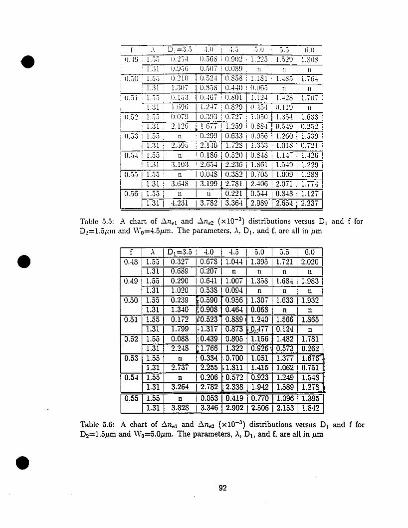
• f ,\ D:-:,.·j ·1.1J :1..j ·j.lJ' i.·j fi.11
Il. I~J ,I.'"j (1.2j·1 ILiGS i 1J.!)1J2 , 1.22i : J..52!! . I.SIJS1.:)1 1J.!Jje· 1J."llï i Il.IlS!) Il Il Il
,'-;-:"IJ.-=,,;-:"1)-'-;1"""'.5=-=,jc7:-:(7"")~:;c,[;7I):-!!-:IJ7"".,=:j~~)-I~! Il.3''8 ; l.lSI: US" i 1. ïG-I •i 1 U 1 i I.:lllï 1 II.S58 IIL-I-Ill ' Il.OG'' , Il 1 Il
c-:1;-:"1.-=,j7"i-'-;l"""'..-=-=,,,c7.-:(7""1.";":['-"":';--;I-:(7""I..7:ju"'"',:-, 1).,~01 1l.l2.j , l.·12S ' l.ïOï i
UI l.G9(j 1 l.2-1ï i 0,82!) lJ..ji-l' IJ, [I!!: Il
i 1J.,j2 I.,ji i Ollï!) 1 O.:3fJ:3 : 0, ï2ï : 1.051l 1.:35·1 i I.G:3:3 i, 1.:31 i 2,12G 'I.Gïï 1 1.25!) : O,SS·j 1 ll':j-l!) 1 0.252
l
, Il.,j:) I.i" i Il : 0.2!)9 10.G3:3 i O.%G i 1.2Gll Li:)!), I.:lI i 2,j!)" : 2.I-IG l1.ï28 1 1.:3i:3 i 1.0181 0.ï21: 0 j-l [55 1 Il 1 0 18G 1 0 i"1l 1 0 S-I8 i 1 I·jï Il -l''G
1
.' - -1.:31 1 :3.l0:) , 2.65-1 2,2:36 i 1.861 i 1.5-1!) 1.229
1 0.5,j J..55 1 Il 1 Om8 0.382 1 O. ï05 1 1.009 1 1.2881 1.:31 1 :3.G-I8 1 H99 2.ï81 1 2.-106 1 2.0ïl 1 1.ïï-l1 1
0.56 1 1.-5.5 i Il 1 Il i 0.221 0.5-1-1 ! 0.8-18 1.12ï i1 1.31 1 -1.231 13. ï82 13.36-1 2.989 1 2.65-1 . .) ')3- 1_.- ,
•Table 5.5: A chart of ~nd and ~n<2 (xl0- 3) distributions versus DI and f for0~=1.5'111l and \\'o=-I.5I'm. The parameters, ,\. Db and f, are ail ill l'm
f ,\ 101=3.5 i -1.0 1 -1.5 1 .5.0 1 'J.;) 1 6.01 1
0.-18 1.5i 1 0.32ï 10.Gi8 1 1.0-1-1 i 1.395 i l.ï21 1 2.020 11.31 0.689 10.20i 1 Il 1 Il 1 n 1 Il 1
0.-19 1.55 0.290 1 0.6-11 1 1.00i 1 1.3·58 1 1.68-1 1 1.983 1
1.31 1 1.020 i 0.538 0.0941 n 1 Il 1 Il
0.50 1.55 0.239 . 0.590. 0.956 1 1.307 1 1.633 1.9321.31 1.340 ;0.908 ' 0.464 0.068 n n
0.51 1.55 0.li2 I~O -')3 0.889 1.240 1.566 1.865.~ .0-
1.31 1.i99 ,: 1.31i 0.8ï3 . OAii 0.124 n0.52 1.55 0.088 )0.439 0.805 1.156' 1.482 1.ï81
1.31 2.2-18 '1.766 1.322 0.926 ~ 0.5i3 0.2620.53 1.55 n 0.334 O.ïOO 1.051 1.3iï 1.6ïo,
1.31 2.i3i 12.255 ,1.811 1.415 1 1.062 1 0.i51 l
0.5-1 1.55 n 0.206 .0.572 0.923 1.249 1.548 '1.31 3.264 2.i82 '2.338 1.942 1.589 1.2ï8
0.55 1.55 n 0.053 0.419 O.iïO 1.096 1.3951.31 3.828 3.346 2.902 2.506 2.153 1.842
•Table 5.6: A chart of ~nd and ~n<2 (XIO-3) distributions versus Dl and f for02=1.5I'm and \Vo=5.0l'm. The parameters, À, Db and f. are ail in l'm
92
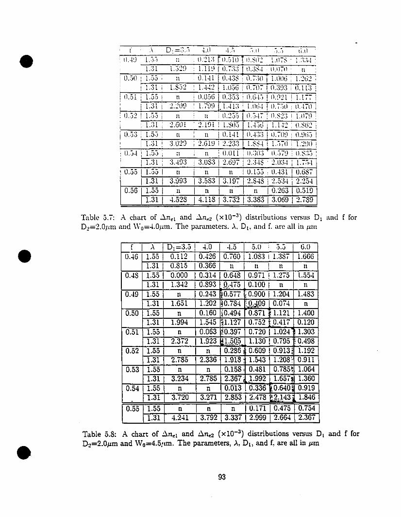
• i 0.::;0 : 1.55: n 0.14110.4:38: ù.7:30 l.lHIG; I.~G~ ;, 1.:31; 1.8·:;2 : 1.-1':2 1 I.U::;6 : 0.707 ! 11.:J~):3 i lUt:3 :
i il.::;1 :-.i71.:.:;5.;.::;-,i--:;~n~-;-.~1).:.;.0~5;;;6-t1-:{;-:')':7c3::;;.:;:3c-:,-I-::-)';.G',;...I.-~'~!:.,.iJ.:.:::~1.;2.:..1-,-!.,:1:..:.1,.:::7~7i1.311 2.209 '1.7991.1.41:;~ 1.1Itj·l!I).7:j1): IU70 i
i il.::;:3 i 1.5.) : n n 0.141 O.4:n 1 Il. 700 : 11.~)li.) !. 1 1.:31 i :3029 ; 2.610 2.2:3.1 1.88·1 1 1.·-,70 i 1.2!)1) !IO.::;4! 1.5::; i n Il ll.llli i Il.:;11:3 11·;70· Il S:l.; :, ,
1 1.:31 , :J..j9:31 :3.08:3 2.6071 2.:3·18 . 2.U:.3·1 , 1.7:;·11 , i
0.55 1 1.55 1 n 1 n n 1 0.155 : ll.-i:31 1 Il.G87,1 1.31 1 3.993 1 3.58:3 3 19- 1 .) S-I8 ..) -'3·1 ' .) .)~ 4
• • _.0..;' ! _.,J. 1 _._0
0.56 1.5.:; 1 n 1 n 1 n 1 n 1 0.263 10.5191.31 1 4.528 1 4.118 1 3.732 13.383 1 3.069 1 2.789
•
•
Table 5.7: A chart of ~nel and ~n.2 (x10-3) distributions ,'ersus Dl and f for02=2.0ILlll and \Vo=4.0Iun. The paramcters. ,\. Db and f. are aU in IUIl
fiA 1 0 1-3.5 1 4.0 1 4.5 1 .:;.U , ·J.V 6.n'(J.~6 1.55 1 0.112 1 0.426 0.760 1 1.0S:3 i US7 1 1.666
1.31 0.815 10.366 n 1 n 1 Il n,0.48 1.55 1 0.000 1 0.314 0.648 0.971 ! 1.275 l.55·1
1.31 1 1.342 10.893 P..A75 0.1001 Il 1 n0.49 1.55 Il 0.243 ~0.577 : 0.900 11.204 1.483
1.31 1.651 1.202 10.784 '.Q:.iQ9 0.074 n0.50 1.55 n 1 0.160 ~0.494 0.8ï! . 1.121 1.400
1.31 1 1.994 1 1.545 ~1.127 0.752 : 0.417 0.1200.51 1.55 n 0.063 W.39i 0.720 1 1.024, . 1.303
1.31 2.372 1.923 . 1.5Q.~ 1.130 1 0.795 " 0.4980.52 1.55 n 1 n 0.286 · 0.609 1 0.913; 1.192
1.31 2.785 2.336 1.918, · 1.543 1.208': 0.9110.53 1.55 n n 0.158, · 0.481 0.785~ 1.064
1.31 3.234 2.785 2.367' 1.992 1.657j 1.3600.54 1.55 n n 0.013 0.336 ,0.640' 0.919
1.31 3.720 13.2ï! 2.853 2.478 •2.143 1.846
0.55 1.55 n n n 0.171 1 0.475 0.7541.31 4.241 3.792 3.337 2.999 1 2.664 2.367
Table 5.8: A chart of ~nel and ~n.2 (x10-3) distributions versus Dl and f for02=2.0j.Lm and Wo=4.5:Lm. The parameters, A, DI> and r, are all in j.LIn
93
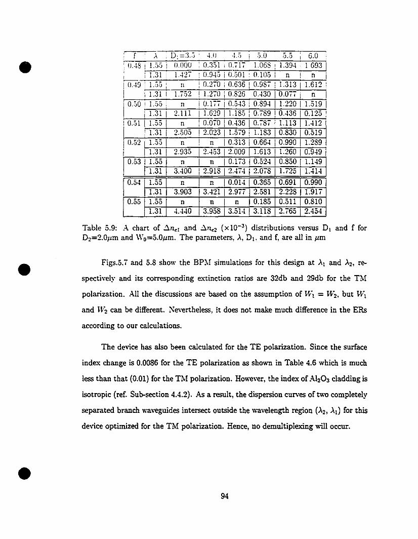
,
1 0.·')0 1.55 i Il i 0.177 1 0.543 1 0.894 1 1.:220 1 l..519 1
1.31 1 :2.111 1 1.629 i 1.185 : 0.789 1 0.436 1 0.1250.;1 1.55 1 n : 0.070 1 0.436 1 0.787 1 1.113 1 1.-112
1.31 1 :2.505 1 2.0:23 1 1.579 1 1.183 1 0.830 1 0.5190.5:2 1..)5 1 n : n 1 0.313 1 0.66-1 1 0.990 1 1.289
1 1.31 1 :2.935 1 2.4.53 1 :2.009 1 1.613 1.260 1 0.9-190.53 1.55 1 n 1 n 1 0.173 0.52-1 1 0.850 1 1.1-19
1.31 1 3.400 1 2.918 1 2.47-1 2.078 l.ï25 1 1.-11-1
0.54 1.55 n 1 n 1 0.01-1 0.365 0.691 0.9901.31 3.903 3.421 12.977 2.581 2.228 1.917
0.55 1.55 n n 1 n 0.185 0.511 0.8101.31 -1.4-10 1 3.958 1 3.51-1 13.118 12.765 2.454
: f ,\, D: -3.,,' 4.0 ~.; i ·).0 5.5 1 6.0 :: 0.·18: 1.',5 j f1.000 • 0.351, (J.717 : 1.068: 1.39-1 i 1 693 1
1 i 1.31: 1.4:27 : (J.9·1:; i 0.;01 i 0.10.) in! n ijiJ::ï9 [ 1.:;5: Il : 0.:270 i 0.636 : 0.987 1 1.313 : 1.612 1
1 \ 1 31 1 1 752 1 1 270 " 0826 1 0430 1 0077 1 n 1
•
•Table 5.9: A chart of ~n<1 and ~n.2 (x 10-3 ) distributions versus Dl and f forD 2=2.0J.tm and \Vo=5.0!lm. The parameters, >., Db and f, are ail in !lm
Figs.5.7 and 5.8 show the BP~r simulations for this design at >'1 and >'2, re
spectively and its corresponding e.'Ctinction ratios are 32db and 29db for the TM
polarization. Al! the discussions are based on the assumption of W1 = to/'2, but W1
and W2 can be different. Nevertheless, it does not make mueh differenee in the ERs
aeeording to our caleulations.
The device has also been ealeulated for the TE polarization. Sinee the surface
inde.'C change is 0.0086 for the TE polarization as shown in Table 4.6 which is much
less than that (0.01) for the TM polarization. HO\\'ever, the inde.'C of AI20 3 dadding is
isotropie (ref. Sub-section 4.4.2). As a result, the dispersion eurves oftwo completely
separated branch waveguides intersect outside the wavelength region (>'2, >'1) for this
deviee optimized for the TM polarization. Henee, no demu\tiplexing will occur.
•94
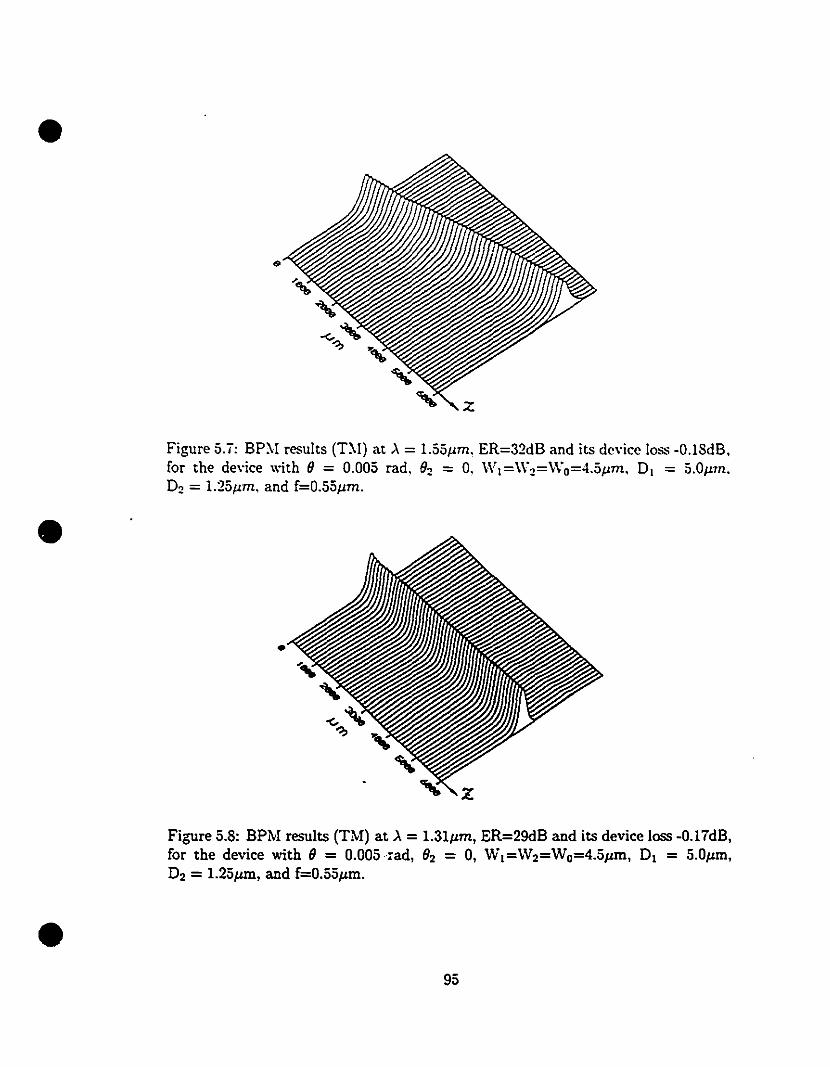
•
•
•
..
Figure 5.i: BPM results (T~I) at ,\ = 1.55Jlm, ER=32dB and its dC\'icc loss -O.lSdB,for the device with 9 = 0.005 rad, O2 = 0, Wt =W2=Wo=4.5Jlm. DI = 5.0Jltn.D2 = 1.25Jlm, and f=0.55Jlm.
•
Figure 5.8: BPM results (TM) at'\ = 1.31Jlm, ER=29dB and its device loss -0.1idB,for the device with 0 = 0.005 ":ad, O2 = 0, W I =W2=Wo=4.5Jlm, DI = 5.0Jlm,D2 = 1.25Jlffi, and f=0.55Jlm.
95
• 5.4 Fabrication
•
•
B..fun' II", fabricatiun. a gl;L'S substrat" h;L' ta be weil c1eaned. The c1eaning
proc"dut<' is standard [3j. CI;L'S slid"s made by Fisher Scientific Co. \\'l're used as
th.. substrates. The substrate cJeaning and most of other fabrication process were
performed in a suitable cJean-room environment. Both ..\l-deposition by thermal
e\';lporation and Alz0 3 deposition by RF sputtering were carried out in a Cooke
\'acuum system. The photo-mask alignment and contact printing were carried out in
a Cobiit photomask aligner.
5.4.1 Initial fabrication process
The initial fabrication process is illustrated in sequence in Fig.5.9. Two photo
masks were needed for fabricating each device saml'le. The first one as illustrated
in Fig.5.10 was used for the first K+ ion-e.,change ta form the branch 0 and the
branch 1. The figure illustrates only one of the three devices. They are parallel ta
each other on the mask \\;th a difference only in the wavguide width 4.0~m, 4.5~m,
and 5.0~m respectively. The effective waveguide depth and the width are 0\ and
Wo= W\ respectively. The second one as illustrated in Fig.5.Il "';as used for making
branch 2 by K+ ion-e.,change and then by sputtering an AI203 layer on the top,
where "'0 = ~\t2' The second mask has to be aligned ....;th the device which has been
made through the first K+ ion-e.,change. The diamond marks in both the masks (see
Figs.5.10 and 5.11) are for alignment. The branches are bent out-wards with an angle
ct (=0.01 rad) arter the two branches are weil separated (20~m) to shorten the device.
Thus, if the final separation of the two branches at the output is to be set to 250~m,
the de\;ce will be about 2cm long. The descriptions of the fabrication steps are given
as follows.
96

•
•
•
•
.) PIHHtH·t':..;i:-;r l"llatillg
Fir:-:t. ,1 -4:1 mixtlll'l' (If phllt(~n'~i:-'t \~hipl\'.\·: alld :l:inllt'~' \~h:jli\'\ .\/' \\';\.... '[\'_
pù:,irl'd (Hltl) tilt' ahl:u::l1all :-'llrLl\'(' '11' tll\' :-illb:-;tLl!t' il.\· :'j1lll-t't1<l111l":" ;\: :~\111\l
HP}'l fur ~t) :"'P...·,ltltb. ;l:ld tb'll. klkitlg. tlll' l't'snltill;!. libn f\l!" :~lllIlillll:\'.... u ."'ll"
C (pn·.bakingL
3 r\' "XPOSlll"('
.-\frt'l' prt'-IJ{l~iIlg. tilt-' tir~t phoru-mask wa~ lI~t'd hl l'Xpd~t' th,' lt'sis! !d t"\" Ikht
thwllgh the mask ùp,'ning, fur SO-llll s"cunds.
4 De\"elopment
Development of the resist was clone in a 2:1 mixture of "!icropùsit d,'w1ùp"r
and D.l. water for -10-GO seconds (depen,ling on the fr','shll"ss ,)1' Ih,' solllti,}n) .
res1l1ting in the remo\'al of th" r"sist frolll the l'\' ,'xpos"l1 al't'as. TIlt'n. th"
sample was baked fur :30 minut"s at 12()" C t.o han["n t.h" n'sist pa tI "rn (post·
baking).
5 Etching
The aluminum was etched away l'rom the areas unprotected by the resist by
immersing it in a solution of phosphoric acid, nitric acid. acetic acid. and Dl
water (16:1:2:1) for 2·10 minutes depending on the freshnl'ss of the solution
and the thickness of the aluminum film. The etched pattern was occasionally
checked under a microscope during the proccss to make sure that the pattern
was l'rel' l'rom residues of Al.
6 Photoresist removal
The photoresist was remo\'ed by immering the sample in a remo\"er solution
(~Iicroposit remover diluted with DI water 1:1),
9ï

•
•
•
i~:'\o., ,al: W;l' 1",ld in a ':f'P! crucihlf' insid~ a \'prtical furnacc. Aft~r th~
,ah W;l' \\"t,II moltl'n at T=.1S:;=1"C. th,' ,amp!,· was put insidp th~ furnac~ to
warm up for 10 min. Thcn. tll<' samp!p wa.' dipp~d into th~ molt~n salt and
til<' dipping tim~ W'"' couIlt~d. Th~ sample was taken out immediate!y when
th.. d.'sin'd tim,' was rpach,·d. Th~ four ion-pxchanged diamond ar~as became
swoIipn du~ to th~ str~ss in th~ sllbstrat~ induced by the ion-exchange [6] but
arc not \'isibI~ und~r the microscope.
8 The aluminum mask was completely etching away in the etching solution as de
scribed in Step 5.
9 An a1uminum thin film (0.05tLm) was deposited on the top ofthe sample to prepare
for the next photomask a1ignment. After depositing the Al-film, the four swollen
diamond areas in the substrate will be clearly visible under the miroscope, and
hence, can be used for a1igning the second mask.
10 Photoresist coating, same as in Step 2 e.xcept the pre-baking for 20 minutes at
so·e.
11 UV .:xposure, same as Step 3 e.xcept that more care should be taken for the
a1ignment. It is designed in the two masks that the two branches are aligned
with a designed angle when the diamonds are aligned ~ith each other between
the two masks. Here, the alignment is done by aligning the diamond marks on
the second mask \\ith the swollen diamonds on the substrate.
12 De\-e.lopment, same as Step 4 but no post-baking.
13 Aluminum deposition by thermal evaporation, same as Step 1.
14 Lift-off
The photoresist together ~ith the Al on its top was removed by immersing the
98

•
•
•
15 The sampI\' wa,..' dippt'd intd tlIt' t,tchin~ :-'llll1tillIl fur a :-olu)rt pt'ri\}d ur llUIt' whidl
is ~nough 10 Neh away th" .-\1 tbin-tillll llSt',j f<lr tilt' patt"m \·isllali/ali,'n III
Stl-..p 9. sa that thr' parts hl Ill' illIl-t·xdl'Ul.~t'd (brandi ~ and tlhl:-'t' dl~Ulltllld:,,)
ar~ cOlllpletel~' op~n\'d l,'a\"ing olh,'rs n)\"t'r"d by allllllinlllll (S"t' Fig.;I.~l1.
16 K';' ion-exchange for Iuakirlg branch tWLl. the prl)('t'~'" bt'ing tht' :,aUh' OL.... in Stt'P 7.
1ï Photoresist coating as in Step 2.
18 l'Y exposure from the back of the substrat" for 90 St'contis.
19 De\"elopment as in Step -1.
20 Ah03 depostion by RF sputtering
After high \"acuum was reached ln the chamber. a mixed gilS of argon and
oxygen (80:20) from a gas cylinder was let in with pressure set to 12 PSI in the
pressure gauge on the gas supply cylinder. By adjusting the high \"acuum valve,
the pressure of the f10wing gas as indicated in the pressure gauges in the vacuum
system was kept Olt 20 micons (1 micro=1 x 10⁻³ torr) i:lSide the chamber and
50 micons in the intake of the mechanic pump. Once the air f10w was stablized,
the RF power was turned on. A tight would be on after the RF unit had been
warmed up to the normal stage. The RF output was then switched on and its
power was tuned ta the desired level. 1'ow, a plasma should be clearly seen in
the chamber. By tuning the two capacitors of the impedance matching circuit,
the reflected power was reduced to a minimum. The shuttle, which usually
covers the A120 3 target when it closes, was kept closed for 20 minutes ta warrn
up the system or stabili2e the plasma after the plasma was established. Once the
shuttle VIas opened, timing was started. During the sputtering, the input power
99
•
•
.'
•
(or the larget voltage). the impedance matching, the water cooting system. and
the gas f10w were checked every half hour.
21 Photoresist remo\'al as in Step 6.
22 The sampIe was eut by a diamond cutter for the device to provide good coupling
for the input and output light. Smoothly eut edges are always needed for good
coupling.
23 Aluminum etching as in Step 5 but with the etching solution heated on a hot
plate to speed up the process.
As we can see that to form the AI-mask for the second K+ ion-e.xchange, we
used a lift-off technique which is more complicated than the process (direct etching)
used to form the AI-mask for the first K+ ion-e.xchange. However, if the direct etching
technique is adopted, the second photo-mask should be the negative of the one shown
in Fig.S.Il. Thus, the second mask has only the diamonds and the second branch
open. They look like small dark diamonds and a dark line respectively under a
microscope since they are very small (in the scale of micrometer) and the rest of
mask made by chrome strongly refiects the light from above. The pattern on the
sample substrate undemeath the second mask can be hardly seen from the above.
Therefore, it is almost impossible to align the the pattem made by the first K+ ion
e.xchange with the mask ",ith ooly the second branch and the diamonds open provided
we make the four diamond areas much larger. ACter the second K+ ion-exchange, a
photoresist film \Vas used to cover the AI mask. There are two purposes for making
tbis film. One is to ease the removal of unwanted Al20 3 after sputtering and the other
is to protect the aluminum from the bomdbardment of high power Ah03 molecules
splashing from the Al20 3 target, since the gigantic chain of the photoresist is much
hea~ier than an Al-atom.
100
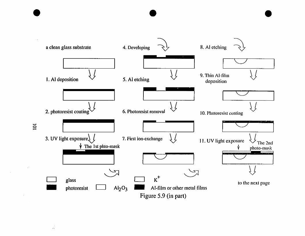
• • •
ta the next page
9. Thin AI-filmdepositiol1
8. AI etching ~
1 C7 1
li1 C7 1
10. Photorcsist coaling V
[C5 1
II. UV Iight expasure V The 2nd
1 b "ho,"-",,,,, 1
VK+
AI-film or other metal films
1 J
1 1
V
1 \:=/ 1
~oFigure 5.9 (in part)
5. Al elching
4. Developing ~
1 1
V
6. Photoresist removal V
Al203Dglass
pholoresisl
1 1
V
1 1
1 1
1. Al deposilion
a c1ean glass subslrale
D-
2. pholoresisl COalingV
3. UV lighl exposureV 7. First ion-exchange
t The 1st phto-mask
~~
....o....
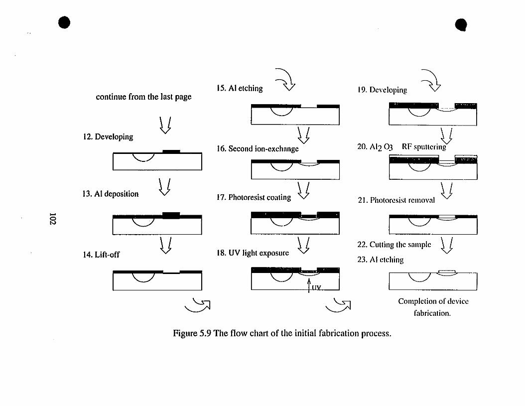
• •continue from the last page
~
Complclion of dcvicc
fabrication.
1C7 C3 J
21. Pholorcsisl rcmoval V
19. Dcycloping
lOC=;I22. Cutting thc samplc V23. AI ctching
r=';?ld 1
20. AIZ 03 RF sPllttcrilY
~J
~
LO':t: 1
LSJ'd118. UV Iighl exposure V
~15. AI etching V
1 <::J 1V
16.Secondion-exchange
I<::JC::JI17. Pholoresisl coaling V
v1 C7 1
V
1 <::? 1
~
1 <::> 1
V
12. Developing
14. Lift-off
13. AI deposilion
-la
Figure 5.9 The flow chart of the initial fabrication process.
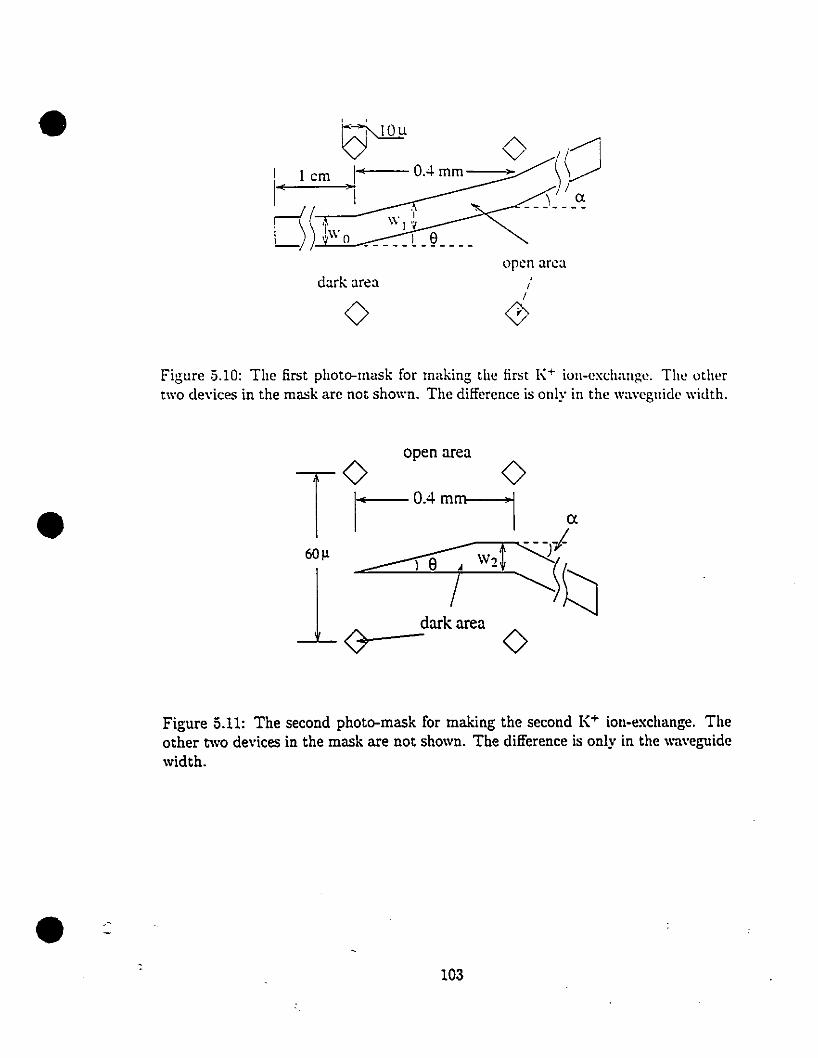
•clark area
<>
open area1
1
<7
•
• :
Figure 5.10: The first photo-mask for making the tirst K+ iOll-exc.:hange. The othertwo cle\·ic.:es in the mask are not shown. The difference is only in the wavegnicle witlth.
Figure 5.11: The second photo-mask for making the second K+ ion-exchange. Theother t\Vo devices in the mask are not shown. The difference is only in the waveguidewidth.
103

• :\llIlllilllllll \\'0 Il Id tlll'l! abo 1", dt'[Josited Ol! t.he smfact' of brandi 2 \\'itho1lt. a pho-
r."n~sist filIn"s protf~cr.ion. resnlting in a highly lassy wLLveguide.
sereen
R
the tirsr dark lino \
~ rluiffractionr ",;-pattern
1;)-----=.-~-\
/
sample
'" ,~laser boam 11 .--7
-----?
'~I ~
le
•Figure 5.12: The width measurement of an aluminum-mask window by slab diffractiontechnique.
Sefore each ion-exchange. the window width of the aluminum ma.~k was mea
sured by a slab aperture diffraction pattern measurement method which is schemat-
icaUy shown in Fig5.12. The AI-mask window for a waveguide is taken as a slit. Its
width W is related to the distance L between the two first-order dark lines of the
diffraction pattern by
IV = ,\ (5.5)sin(tan- I (2~)]
where R is the distance from the mask surface to the screen on which the pattern is
measured and ,\ is the wavelength of a laser light source. In our set-up, ,\ = 0.6328J.lm
and R=2 m were chosen, which led to a measurement error about ~VV = OAJ.lm.
•104
• 5.4.2 l\Ieasurement set-up
Thl' measurcmcnt set-up uSl'd to wst 0\11' de"iees is shown iu Fi~.;;.l:l. Th,'
light Cüupling was realized b,' a liber butt-coupling technique. TIll' lllltpllt light was
t"oclls:-:ed \ ~a a Illicro (20 x) ll'n~ to fornl an itnagc in a Hamatuat:-Oll \"idpt) l';Ullt'ra.
Thl' __ id!'o signais were. tlll'n. sellt to an oscilloscope from which th,' ERs mnid hl'
measure,l. The Iight spots from the two hranches wt'n' displayed as t\\"() sl'paratl'd
pt'aks on thl' oscilloscopp scrl'en. If \'1 and \ ~ rt~prcsl'nt the heig,hts ,,1" the I"'ab I"rom
ImUlch land hrancll 2 respecriwIy. the ERs in db arc dl'iined by
(;;.6)
•
•
A He-l'e laser emitting light at -\ = 0.632Sllm was used to align the light
coupling. Before measurement. the -\ =0.632SIl laser light was coupled into a liber
end b,' a long focusing lcns...\rter thc output spots from the branchl's Wl'l'l' obst'l'\·ed .
the inpnt-cnd of the liber was rcmoved from the -\ = O.632SILm laser source and
plugged into a '\1 or -\2 laser diode source. The light coupied into the de\'ice from
the liber "'as considered randomly polarized. A polarizer bet",een the object leus and
the video camera ",as used to get TM modes output only by positioning the polarizer
perpendicnlar to the waveguide surface.
105
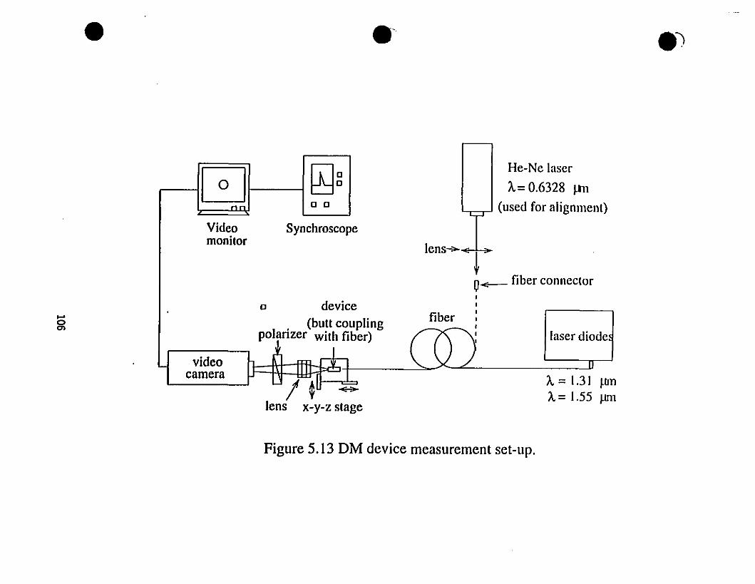
• .- el
Â. = 1.55 J1Il11 ~u ~Jens x-y-z stage
He-Ne laser
G ~g À= 0.6328 ,..nMM c c (used for alignmenl)
Le-'
Video Synchroscopemonitor
Jens~
~0- fiber connector1
c device 1
fiber1
. (bull coupling 11
poJanzer with fiber) CO) laser diode!1 1
- video " lTT1 VI 1 IlIIIcamera ~ ~d~ 1 Â. = 1.31 wn
....oCl)
Figure 5.13 DM device measurement set-up.
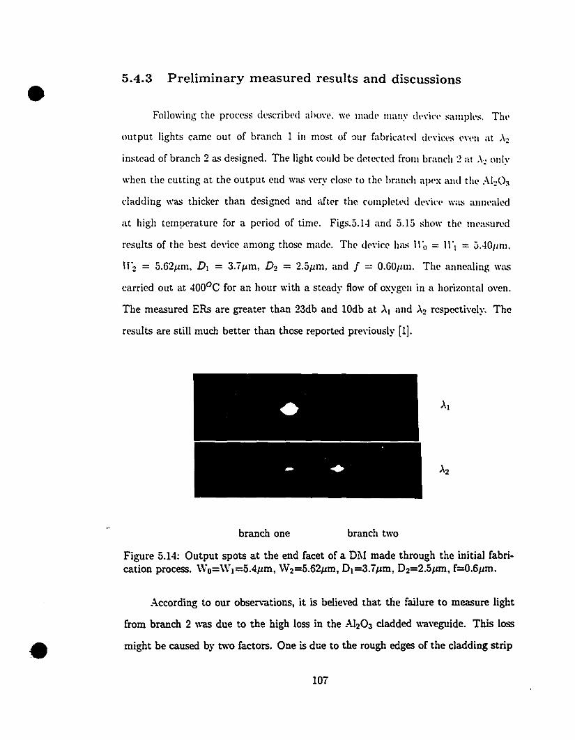
• 5.4.3 Preliminary measured results and discussions
Following the process dc~crÎbl'd aho\'!'. Wl' made many d!'\'ic!' sampl,'s, Th!'
output lights came out of branch 1 in most of :)ur fabricat!'d dl'\'in's l'\"l'n at -\~
instead of branch 2 as de~Îgned. The light çauld be dete,'ted from brandi:! al .\~ only
when the cutting Olt the output end was \'cry do~c to thl' brandI apl'X and thl' :\l~O:,
cladding was thicker than designcd and after t.hl' compll'tl'd devÎn' was annl'aled
at high tem~eraturc for a pl'riod of timc. Fig~.5.1.J and 5.15 show tlll' nll'asurcd
results of the best de\'Îce among those made. The de\'iee has Ir" == lrl == 5AOJIIlI.
11"2 == 5.62pm, DI = 3.i pm, D 2 = 2.5pm, and f == O.GOJlm. The annealing wus
carried out Olt .JOOoC for an hour with a steady f10w of oxygen in a horizontal aven.
The measured ERs are greater than 23db and lOdb at ~I and -\2 respectively. The
results are still much better than those reported previously [1].
branch one branch two
•
Figure 5.14: Output spots at the end facet of a DM made through the initial fabrication process. \~'o=Wl=5.4pm, W2=5.62pm, D1=3.ipm, D2=2.5pm, f=O.6pm.
According to our observations, it is believed that the failure to measure light
from branch 2 \Vas due to the high loss in the AI20 3 cladded waveguide. This loss
might be caused b~' two factors. One is due to the rough edges of the cladding strip
lOi
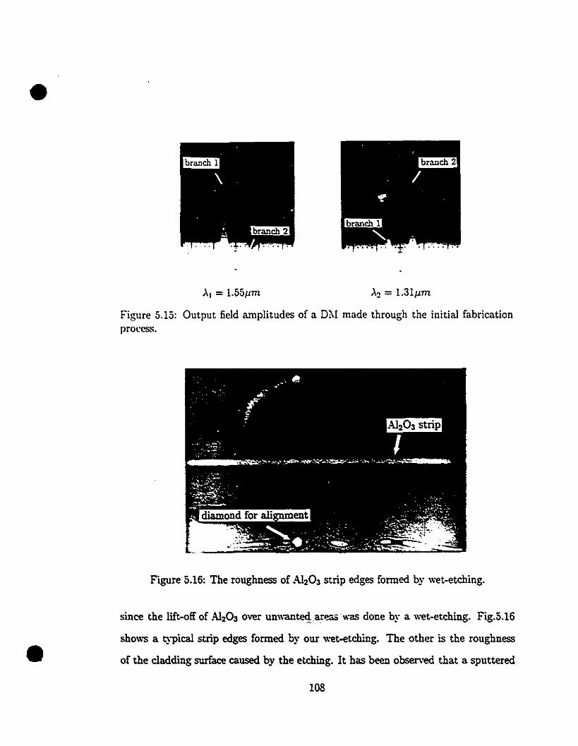
•
•
Figure 5.15: Output field amplitudes of a Dl\! made through the initial fabricationprocess.
Figure 5.16: The roughness of Ah03 strip edges formed by wet-etching.
since the lift-off of A1203 over unwantedar~was done b~' a wet-etching. Fig.5.16
shows a ~1>ical strip edges formed by our wet-etching. The other is the roughness
of the cladding surface caused by the etching. It has been observed that a sputtered
lOS
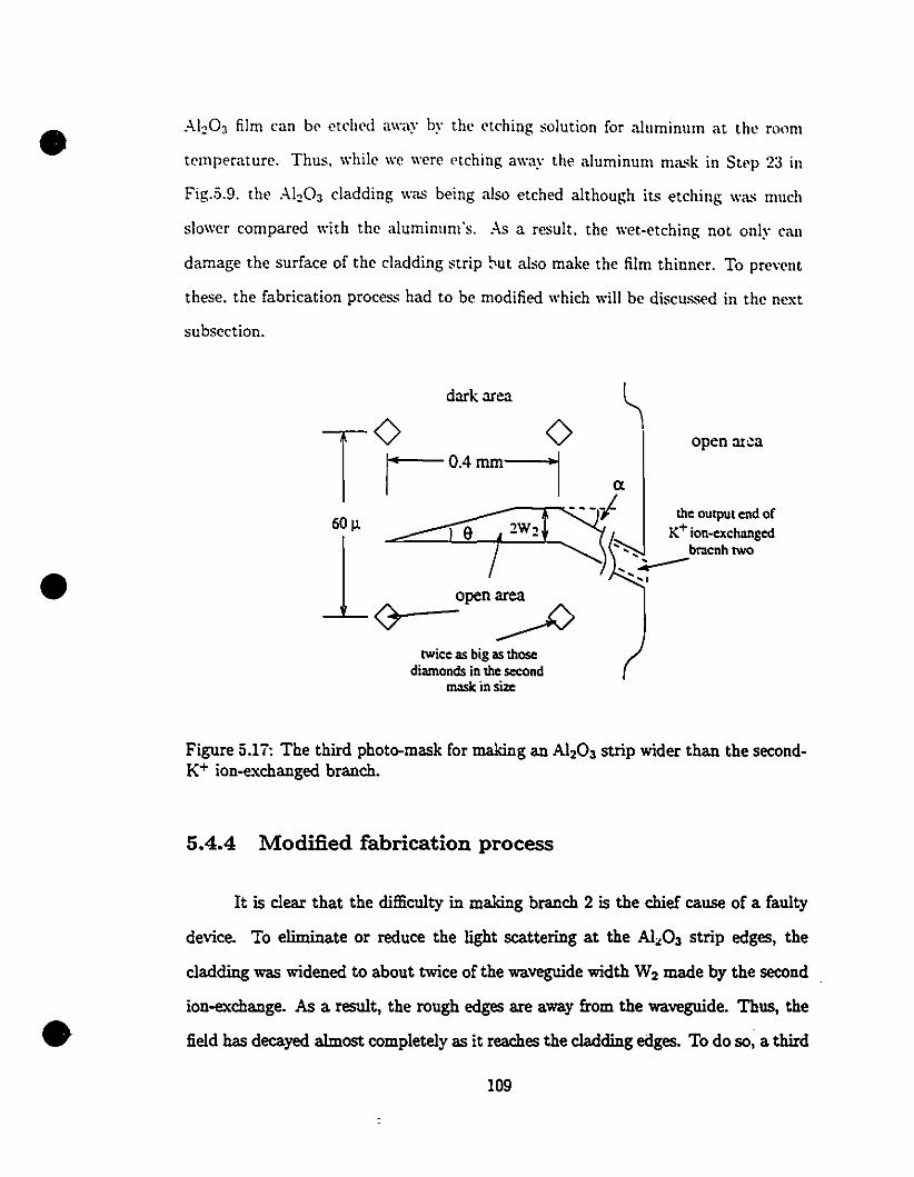
• .-\lzOJ film can b~ Nch~d a\\"ay by the Nehing solution for aluminum at the room
t~mpcrature. Thus. \\"hile \\"e \\"ere Nehing a\\"ay the aluminum ma.,k in Step 23 in
Fig.5.9. the AI20 3 cladding \\"as being also etched although its etching was Illueh
slower compared with the aluminum·s. As a result. the wet-etehing not only l'an
damage the surface of the cladding strip ~ut also make the film thinner. To prevcnt
these. the fabrication process had to be modified which will be discussed in the next
subsection.
open ar~To °,0.4mml a
o ~---I the OUlpUI end of
16 Il.~ K+ion-exchnnged
.......... bracnh IWO- ....----,openarea
~- ~!Wice us big us thase
diamonds in the secondmnsIc in size
dark area
•Figure 5.1i: The third photo-mask for making an Ah03 strip wider than the secondK+ ion-e.xchanged branch.
5.4.4 Modified fabrication process
•
It is clear that the difliculty in making branch 2 is the chief cause of a faulty
device. To eliminate or reduce the iight scattering at the Al.03 strip edges, the
cladding was widened to about twice of the waveguide width W2 made by the second
ion-exchange. As a resu1t, the rough edges are away from the waveguide. Thus, the
field has decayed almost completely as it reaches the cladding edges. To do so, a third
109
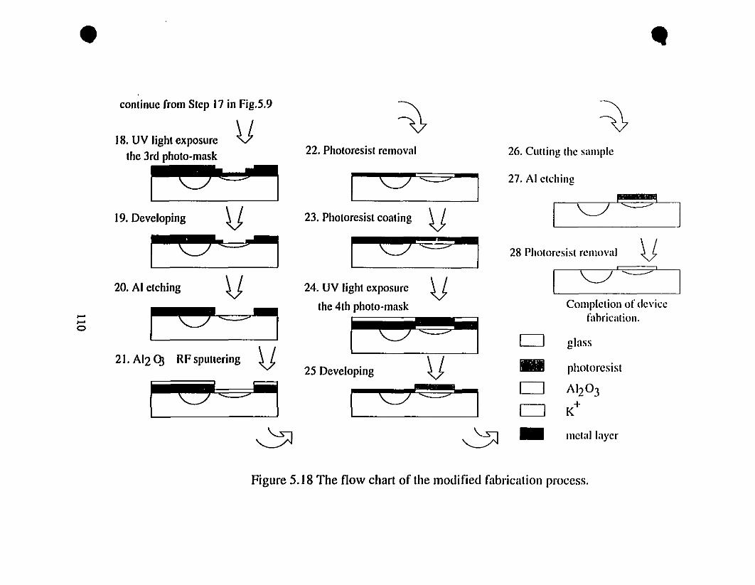
• -conlinue from Step 17 in Fig.5.9
~ ~V18. UV Iight exposure
the 3rd photo-mask 22. Photoresist removal 26. CUlling the salllple
~ 10=
1
27. AI etching
, !
V V 1"--7 =
119. Developing 23. Photoresist coating
Le'::: 1 1O'='
128 Photoresist relllllvai V
1
"--7'= !
120. AI etching V 24. UV Iight exposure VLe=
1
the 41h photo-mask COlllplelion of dcvicc......
r-\?='fahrication .......
0
0 glass
V21. AIZ QI RF spullering V - photoresist25 Developing
r-\?=' 0 A120]
10=
1 0 K+
~ ~ - lIIetal layer
Figure 5.18 The flow chart of the modified fabrication proccss.
•
•
•
photomask i, nl','dl'd whil'h was ,hown in Fip,.5.! ï. For thl' rna.,k alip,null'nt. thl'
diamond, in thl' thirel rnask are' twil'<' as bi~ as thosl' iu thl' ",'coud rnask and th,'
mask is transparent sta:-ting right from thl' ,'mls of ail thl' thr,'" dl'\"ic,'s whieh an'
paralll'lly located on thl' ,ame masks. In thl' mask alignml'nt. thl' op,'n l'nds of
branch two in the 3rd mask are aligned with the K- ion-l'xchangl'd patt,'rns of branch
two. Then. the alignment is checked by the matching of diamonds with thl' K+
ion-exchanged diamond patterns. To protect the AI20 3 film from bl'ing l'tched. a
photoresist film was coated on top of the AI20 3 strip before etching away the last
aIuminum mask. A fourth photo mask may be needed which is exactly the negati\"c
of the third photomask. We can aIso use negative photoresist coating on the top of
the devices and expose it from the back of the substrate with UV light without the
fourth mask.
The modified process after Step l ï in the last subsection is described as follows
and the flow chart for the process is shown in Fig.5.IS.
18 UV light e:'<posure after the aIignment of the third mask.
19 Development, same as Step 4 in the last sub-section.
20 Al etching, same as Step 5 in the last sub-section.
21 Sputtering, same as Step 20 in the last sub-section.
22 Photoresist removal, same as Step 6 in the last sub-section.
23 Coating a positive photoresist (or negative photoresist).
24 "(JV e.'qlosure after the aIignment of the fourth photomask. If a negative pha
toresist were used, the back of the substrate can be UV exposed without a
photomask.
111

•
•
•
26 TIlt' sample was eut at prol"'r locations for the cOllpling in and out of light.
27 .-\1 etching. SaIlle ;L'i Ste!' j in the last sub-seetion.
28 Tht' pilot,ol'l'sisr rt'lIlo\"al. same as Step Gin rhl' la~r. sul'>-St'("tioll.
flJlIowing the fabrication proce~s abm·e. the loss due to the e,lg,' wllghness and
..1.1/)" smface damage can !Je reduced. The de"ice is lllltch impw"ed and the output
light from brandI :2 at ,\~ cali no'" be easily observed.
5.5 Measured Results and Discussions
Fig.5.19 shows the output spots for a de"ice with Wo = n"l = 5.32 ± O.4JLm,
lr~ = ii.02 ± O..lJLm, DI = 5.0 ± O.lpm. D 2 = 1.5 ± O.l/Lm. and f = 0.56 ± 0.02/Lm.
Their field intensities are shown in Fig.5.:20. Their measllred ER ' ..tilles together those
obt.ained by BPM simulations are listed in Table 5.10.
ER(dB) 1 Al 1 '\2measured 1 >25 20
BP~..r 1 26 24
Table 5.10: Extinction ratios for a de\ice with vVo = WI = 5.32 ± O.4JLm, H'"2 5.02 ± 0.4JLm, DI = 5.0 ± O.lJLm, D~ = 1.5 ± O.lJLm, and f = 0.56 ± 0.02JLm.
As shown in the table, the device works weil and provides high ERs. The
measured results basically agree with those calculated from BPM simulations.
The discrepancies between the calculated and measured ER values are mainly
due to the uncertainty in the Al~03 thickness. It is diflicult to control its error less
than ±O.O1. 'vVe can also see that the device parameters are clifferent from those
in the optimized design presented in the pre\ious section, especially the waveguide
widths. In the fabrication, the ion-exchange time can be controlled \\ithin one minute,
112
•
•
•
attll't' T is srablt:' bl't\\'t't'!l :)S~-:;~l;:'C. But fl)t" lb' '.\':ln·~tlidt' \\"idth tilt' ~ltn;ttil.\n 1':';
\'t'r~' rnudl ditft'I't'IlL Thl'l't' ;trt' !llany f;H.:hlr:, \\"illd~ ;ltft·(·t tilt' width tl(" rht' \\";\\'l'~n:(:I'
Illa:-;k. ~l.lch ~L'\ rht' aitullinunl hInt th:l'kul'SS. rhicktw,:.;,:.; Ill' t!h' phut\lrt·,:.;i:--t. l"\' t'Xlh1:'lln'
r.irul'. dl'\"t'loptlll'Ilt rinw. t'rl'hin~ tiIIlt'. :lllllmlifllrmitÎt's tlf th,' altltuillIlBlli!l:l ;tnd l:!!'
pltut.lJrl'sist cuatill~. Tht.' \\"a\'f'~llidl' width is diHiclilt tt) l'tHltl\ll. Tp mak,' .dl th,'
fa bricatcd paranlt~tl'rs tht~ :-lame ;\...'\ BP~r~opr ÎIlliZl',l ,llll'S i:-; n'r~' di tfÎl"ll 1t. F\ ln lI11att·l\',
t.herl' are safl't.~· marg,ins für th":,,, paranll'tl'rs t,) ,'!>tain tl1l' ERs "'·,'r :ln"!>. lt i"
worth nll'Iltiuning that the lint'al" fesponse l'au:.;,' of th., vid"!1 1'<lIllt'ra i~ quitt' litllitt'li.
The power measured might bt' beyond the lint'ar rang" yil'1ding th,· mt'asllrt'd ER.,
somewhat less than the tru" ones.
The de\'ice works \l'el! and can pro\'ide high ERs. HO\l'ewr. the high sensiti\'ity
to the .-\120 3 dadding thickness makes the de\'ice hard to fabricate. A good \l'ay
to O\'ercome this is tu reduce tlH' branl'h angle. For l'xample. if the angl,' i,; l'hosen
t.o ue 0.003 rad. the effectiw index difference of the t\l'O intinitely separated branch
wln'eguides .:1T11 wou1d be less than 0.0002 at _\1 and ~T12 less than about 0.000-1 at
-'2 to achie\'e the ERs O\'er 20 db (sel' Figs.5.5 and 5.6). The fabrication tolerance
to the Ab03 thickness can then be approximately relaxed to ±0.02I'm as wc cali see
from Table 5.1-5.9. As we ha\'e discussed before, the braoch angle is forme<! by two
photomasks' alignment which cao be done without much difliculty. The drawback in
the brandi angle reduction is a required increase in the de\'ice's lengh.
113
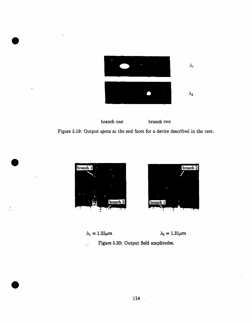
•
branch one branch two
Figure 5.19: Output spots at the end facet for a device described in the text.
•
•
À l = 1.55~m À2 = 1.31~m
Figure 5.20: Output field a:nplitudes.
114
•
•
•
Bibliography
[lJ :\. Goto and G.L. Yip. "Y-branch wavelength multi/demultiplexer for À =
1.30Jlm and À = 1.55Jlm", Electronics Lett., vo1.26, pp.102-103. 1990.
[2] H. Yajima, "Theory and applications of dielectric branching waveguidcs" , in Proc.
Symp. Optical and Acoustical Micro-Elecctronics, pp.339-358, New York, 19ï4.
[3] M. Masuda and G.L. Yip,Fabrication techniques of thin film optical waveguides
using McGilI facilities, A report of McGill Guided-Wave Photonics Lab., Jan.,
1980.
115
•
•
•
Chapter 6
A K+ and Ag+ Ion-exchangedY-branch WDM
6.1 Introduction
In an .~1203 strip loaded Y-branch WDNI discusseà in the last chapter, the re
fractÏ\'e index of A120 3 is much higher than the surface inàex of the K+ ion- exchanged
wuveguide. In view of this, an Al20 3 loaded arm 2 can be made to be relatively shal
low and yet tO yield a strongly asymmetrical Y-branch and a steep intersection of the
dispersion curves of two infinitely separated branches. If the intersection is between
the two wavelengths to be demultiple.'\':ed and the branch angle is sufficiently small
(see Eq.(3.13)), the branch will work as a WDM for these two wavelengths.
Ag+ ion-exchange in a glass substrate has been a weil established technique.
It can provide a surface inde.'\': exchange Don. between 0.01 to 0.09 by adjusting the
AgN03 dilution [1], which is much larger than the surface inde.'\': change Don. = 0.01
by K+ ion-e.'\':change. Thus, if one branch ~ made by K+ ion-e.'\':change and the other
branch is made by Ag+ ion-e.'\':change, a strongly asymmetic Y-branch can be realized.
A Y-branch wavelength multijdemultiple.'\':erwith a configuration shown in Fig.5.1 can
he made by using these two ion-e.'\':changes (K+ and Ag+).
··115
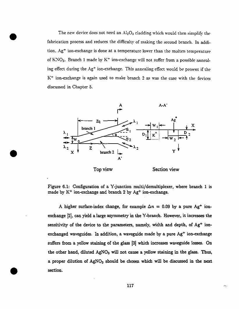
• The new device does not need an A120 3 cladding which would then simplify the
fabrication process and reduces the difficulty of making the second branch. In addi.
tion, Ag+ ion-exchange is done at a temperature lower than the moltcn tcmperature
of K:-i03 . Branch 1 made by K+ ion-exchange will not suffer from a possible anneal.
ing effect during the Ag+ ion-exchange. This annl'aling effect would bl' presl'nt if the
K+ ion-exchange is again used to make branch 2 as was the case with thl' :IevÎCes
discussed in Chapter 5.
•
A
i
À 1
~ a2
- -'--f"':::...--ll-...Jl;c---- --À,_ Z """"À,branch2 l.. -
A'
Topview
A·A'
+Ag
Section view
x
•
Figure 6.1: Configuration of a Y-junction multi/demultiplexer, where branch 1 ismade by K+ ion-exchange and branch 2 by Ag+ ion-e.xchange.
A higher surface-index change, for example .6.n = 0.09 by a pure Ag+ ion
exchange [2], can yield a large asymmetry in the Y-branch. However, it increases the
sensitivity of the device to the parameters, namely, width and depth, of Ag+ ion
exchanged waveguides. In addition, a waveguide made by a pure Ag+ ion-exchange
suffers from a yellow staining of the glass [3) which increases waveguide losses. On
the other hand, diluted AgN03 will not cause a yeIIow staining in the glass. Thus,
a proper dilution of AgN03 should be chosen which will be discussed in the next
section.
117
• 6.2 Chioce of AgN03 Dilution
•
•
A Gaussian function was used to model the index profile of the K+ ion
exchanged waveguide but a second-order polynomial for that of the Ag+ ion-exchanged
one as discussed in Chapter 4. :'\umerical simulations of wavelength demultiplexing
were carried out \Vith the t\Vo-dimensional BP~I together \Vith the effective index
method.
5ince the surface inde;" of branch 2 is the highest of ail indices, the depth of the
Ag+ ion-e;I:changed branch 2, D2 , where the index profile is truncated to intersect the
substrate index (d in Fig.4.13 and FigA.15), is the most sensitive parameter in this
device. Thus, the job of a design optimization is mainly to ma."cimize the tolerance
on D2 while keeping the e."<tinction ratios (ERs) over 20 dB for both \Vaveler.gths.
ER is approximately proportional to Ll.nei (i=l or 2). Thus, a steeper dispersion
CUITe for branch 2, corresponding to a more asymmetric branch, would yield larger
values of ~nei and, hence, e."<tinction ratios at both wavelengths, provided D2 is
properly chosen to ensure that the intersection point of the two dispersion curves
can be appropriately located between the two wavelengths to be demultiple.,,<ed. D2
depends critically on the surface index change ~n. of branch 2. A higher value ~n.
of branch 2 will result in a larger asymmetry of the branch and, hence, higher value;:;
of ER. However, a simultaneous reduction of D2 will also be required to locate the
intersection point between À2 and À! as has been mentioned above. A small change
in D2 will cause relatively larger shift in its dispersion curve due to the larger ~n.
and the smaller D2• Hence, the device's sensitivity to D2 is increased. On the other
hand, a small ~n. value of branch 2 will still make the device sensitive to D2 since a
less steep dispersion curve for arm 2 willleave a smaller tolerance margin for D2 to
keep ERs> 20dB. Thus, between the two extremes, there is an optimal.6.n. of branch
2 to :rield the largest allowable tolerance ~2 in D2.
118
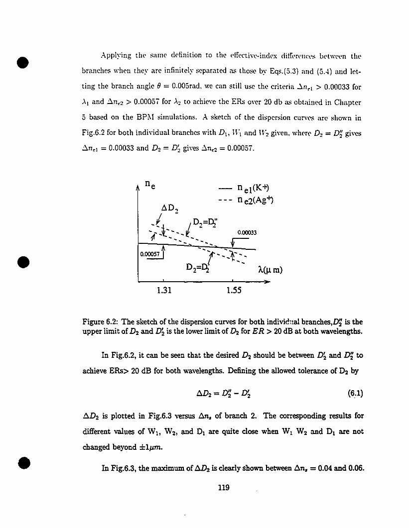
•
•
Applying th~ salll~ d~finition 1.0 th~ ~ff~ctiw-ind('x diffl'rl'nl"'s bl't.w('l'n tilt'
branchcs wh~n t.hcy arc infinitcly scparated as thosc by Eqs.(5.3) and (5..t) and l~t.
t.ing thc branch anglc () = 0.005rad, wc can still usc thc crit~ria ~nd > 0.00033 for
'\1 and ~n<2 > 0.0005ï for '\2 1.0 achicvc the ERs ovcr 20 db as obtain~d in Chaptcr
5 based on the BP:'-' simulations. A sketch of thc dispcrsion curvcs are shown in
Fig.6.2 for both indÎ\'idual branchcs with Dl. Irl and W2 givcn. whcr~ D2 = D~ givcs
~nd = 0.00033 and D2 = D~ gÎ\'cs j.n<2 = 0.0005ï.
À(IJ. m)
1.31 1.55
Figure 6.2: The sketch of the dispersion curves for both indiviè;tal branches,~ is theupper limit of D2 and Di is the lower limit of D2 for ER > 20 dB al. both wavelengths.
ln Fig.6.2, il. can be seen that the desired D2 should be between Di and D~ 1.0
achieve ERs> 20 dB for both wavelengths. Defining the allowed tolerance of D2 by
(6.1)
•~D2 is plotted in Fig.6.3 versus Don. of branch 2. The corresponding results for
different values of Wb W2, and DI are quite close when WI W2 and DI are not
changed beyond ±IJlm.
ln Fig.6.3, the maximum of tJ)2 is clearly shown between Don. = 0.04 and 0.06.
119
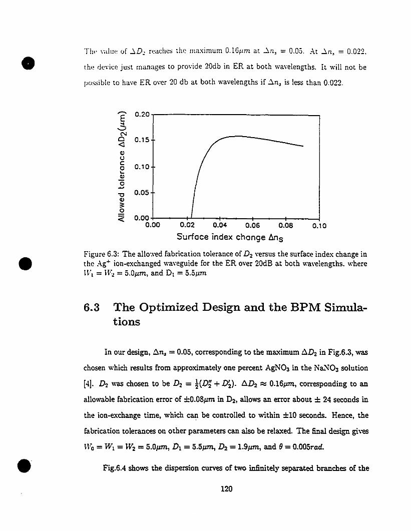
• Tl... \,dl'" of :::'Do n~achcs the maximum O.lGpm at :::'n, = 0.05. At :::'n, = 0.022 .
r.h" d"vicc just manages to provide 20db in ER at both wavelengths. It will not be
possible to have ER over 20 db at both wavelengths if ~n, is Jess than 0.022.
Figure 6.3: The allo·.\'ed fabrication tolerance of D2 wrsus the surface index change inthe Ag+ ion-exchanged waveguide for the ER over 20dB at both wavelengths. wheren'l = ty~ = 5.0pm, and Dl =5.5pm
0.20,-------------------,
0.10
-0.15
O., 0
0.05
0.00-I---+l----+----+-__+-_---I0.00 0.02 0.04 0.06 0.08
Surface index change t.ns
,.....,E::l..........N
Cl<l(1)
uco...(1)
o-
•6.3 The Optimized Design and the BPM Simula
tions
•
In our design, Cl.n, =0.05, corresponding to the ma:'timum Cl.D2 in Fig.6.3, was
chosen which results from approximately one percent AgN03 in the Na.~03 solution
[4J. D2 was chosen to be D2 = HD~ + D;). Cl.D2 ::::: 0.16pm, corresponding to an
allowable fabrication errer of ±O.OSpm in O2, allows an error about ± 24 seconds in
the ion-e.xchange time, which can be controlled to within ±10 seconds. Hence, the
fabrication tolerances on other parameters can also be relaxed. The final design gives
n'-o =W I =W2 =5.0Jlm, Dl = 5.5pm, D2 = 1.9pm, and (} =0.005rad.
Fig.6.4 shows the dispersion CUIVes of two infinitely separated branches of the
120
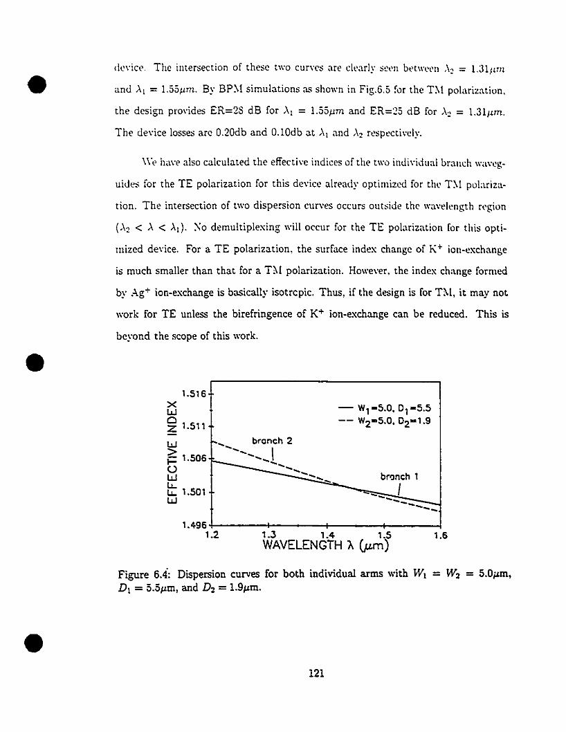
• dc\"icc. The intersection of these two curws are clcarly Sl'l'n bl'twl'l'n .\~ = 1.31 llTTl
and À 1 = 1.55Jlm. By BP~I simulations as shown in Fig.6.5 for the T:-I polarization,
the design pl'O"ides ER=2S dB for Al = L55Jlm and ER=:25 dB for A~ = 1.311Lm.
The de"ice losses are D.2Ddb and D,lDdb at '\1 and ,\~ rcspcctivcly.
\\'p haw also calculated the effective indices of the two indi\"idllal brandi wawg
uides for the TE polarization for this de"ire already optimized for the T~l polariza-
tion. The intersection of two dispersion curves occurs outside the wawlcngth rl'gion
•
(,\~ < À < Al)' ~o demultiplexing will occur for the TE polarization for this opti.
mized de\"ice. For a TE polarization. the surface index change of K+ ion-l'l'change
is much smaller than that for a T"-I polarization. However. the index change formed
by Ag+ ion-exchange is basically isotrcpic. Thus. if the design is for Tl\!, it may not
work for TE unless the birefringence of K+ ion-exchange l'an be reduced. This is
beyond the scope of this work,
1.5'6- W, =5.0. D, -5.5-- W2-5.0. D2-1.9
xwoZ 1.511
W r-_ bronch 2> ---- 1t; ,.506 r-------::-:-::-::2-W -- brlJnch 1l.L. ~---.:::---b '.50' --.",::::--~-_~/::-~---- -----
1.61.3 1.4 1.5WAVELENGTH Jo. (,um)
'.496+----+-----+-----~--__l
1.2
Figure 6.4: Dispersion curves for both individual arms \Vith Wl - W2 = 5.0jlm,Dl = 5.5I-!m, and D2 = 1.91-!m.
•121
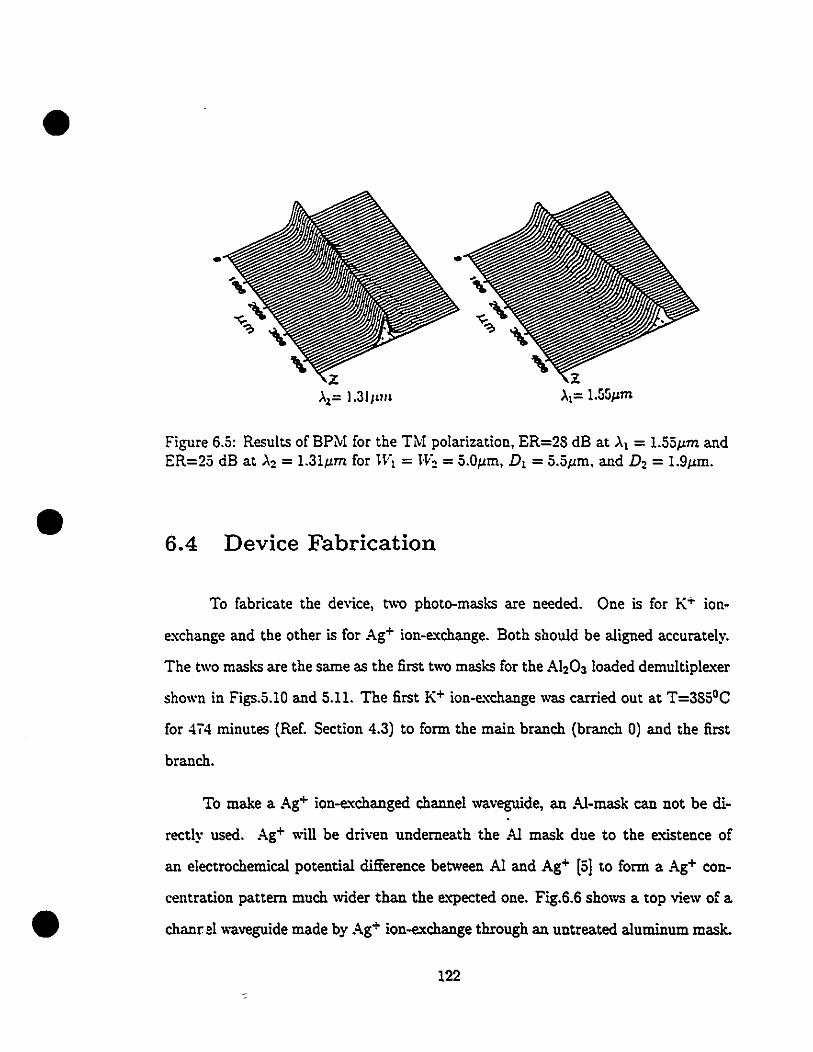
••
•
•
Figure 6.5: Results of BPM for the TM polarization, ER=28 dB at ).1 = 1.55Jlm andER=25 dB at ).2 = 1.31Jlm for WI = H,'2 = 5.0Jlm, DI = 5.5Jlm, and D2 = 1.9Jlm.
6.4 Deviee Fabrication
To fabricate the device, t'l':O photo-masks are needed. One is for K+ ion
exchange and the other is for Ag+ ion-exchange. Both should be aligned accurately.
The two masks are the same as the first two masks for the Ah03 loaded demultiplexer
shown in Figs.5.10 and 5.11. The first K+ ion-e.'Cchange was carried out at T=38SoC
for 4ï4 minutes (Ref. Section 4.3) to form the main branch (branch 0) and the first
branch.
To make a Ag+ ion-e.'Cchanged channel waveguide, an AI-mask can not be di
rectly used. Ag+ will be driven undemeath the AI mask due to the e.'CÏStence of
an electrochemical potential difference between Al and Ag+ [5) to form a Ag+ con
centration pattern much ,vider than the e.'Cpected one. Fig.6.6 shows a top view of a
chanr el waveguide made by Ag+ ion-exchange through an untreated aluminurn mask.
122
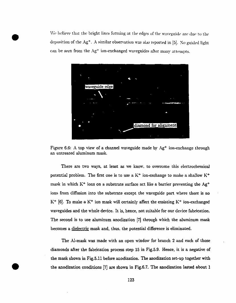
•
•
\\"l' bdil'\'(' that tht, bright Iinl'~ forming at tilt' cdgl'~ of tilt' wa\"l'~uid,' an' dUt' to th,'
ùeposition of the Ag+. A ~imilar observation wa~ aloo n·portt·ù in [r,]. :"0 guidt'd light
can be seen from the Ag+ ion-exchanged w<lwguides after Illany attl'lIlpt~.
Figure 6.6: A top vieil' of a channel waveguide made by Ag+ ion-exchange throughan untreated a1uminum mask.
There are two ways, at least as we know. to overcome this c1ectrochemical
potential problem. The !irst one is to use a K+ ion-e.'Cchange to make a shallow K+
mask in which K+ ions on a substrate surface act like a barrier preventing the Ag+
ions from diffusion into the substrate except the waveguide part where there is no
K+ [6J. To make a K+ ion mask will certainly affect the exsisting K+ iOll-exchanged
wa\'eguides and the whole device. It is, hence, not suitable for our device fabrication.
The second is to use aluminum anodization [i] through which the aluminum mask
becomes a dielectric mask and, thus, the potential dilference is eliminated.
The AI-mask was made with an open window for branch 2 and each of those
diarnonds after the fabrication process step 15 in Fig.5.9. Hence, it is a negative of
the mask shown in Fig.5.lI before anodization. The anodization set-up together with
the anodization conditions [i] are shown in Fig.6.i. The anodization lasted about 1
123

• llJ :3 lIIiUlltl'S. depl'udiug on the thickness of the Al layer. The current. whose "alue is
de!,I'IHlPut on the metal area exposure to the anodization solution. should be moni-
tored during the proccss. The cornpletion of the anodization is indicated by an abrupt
drop of current. The sample was soaked in acetone for a few minutes after a brief
rinsp in DI water. After anodization. the mask (mostly AI20 3 [S]) was transparent
although there were sorne Al metal residues which were unavoidable according to our
experienccs.
power supply anuneler
anode
GJ - :::+1'----;00
15 v
cathode
• ice W3ter
samplemeral lectrode
Figure 6.7: The Al-mask anodization set-up.
•
Then, Ag+ exchange was carried out at T=325D for 3 minutes and 19 seconds.
The anodized AI-mask (now becoming Ah03 mask) could be removed by immers
ing the sample in a commonly used etching solution mbced with H3P04 , HN03,
CH3COOH, and water at room temperature. The fabrication process is described as
fol1ows after Step 15 in Fig.5.9 and the fiow chart is summarized in Fig.6.S.
16 Photoresist coating
124

•
•
•
Th" sampi" was coatl'd by photon'sist :,-' in Stl'p:2 in tlll' snll-Sl'ctiun 5,-1.1. Th,'
photor"sist on the top of tlll' Al-mask windows and tlll'ir vincinity W:'-'. th,'n.
wiped out with a cotton tip '\"l'ttl'd with an'tolll'. TIll' parts uncO\"'n'd wl)uld
be anodized lat"r.
1ï .\1 anodization as described in the second pre\'ious paragraph.
18 Photorcsist removaI. same as Step 6 in the snb-sl'Ction 5.·1.1.
19 Ag· ion-exchange as described in the pre\'ious paragraph.
20 Cutting the sampie
The cutting positions l'an be conveniently locatcd before the AI-l~::.,k (parts of
the AI-mask ",as Ah03) "'as completely etched a"'ay. Other",ise, the device
could not be seen c1early once the AI-mask "'as removed.
21 Etching AI and AI20 3 as in Step 23 in the sub-scction 5.4.1.
125
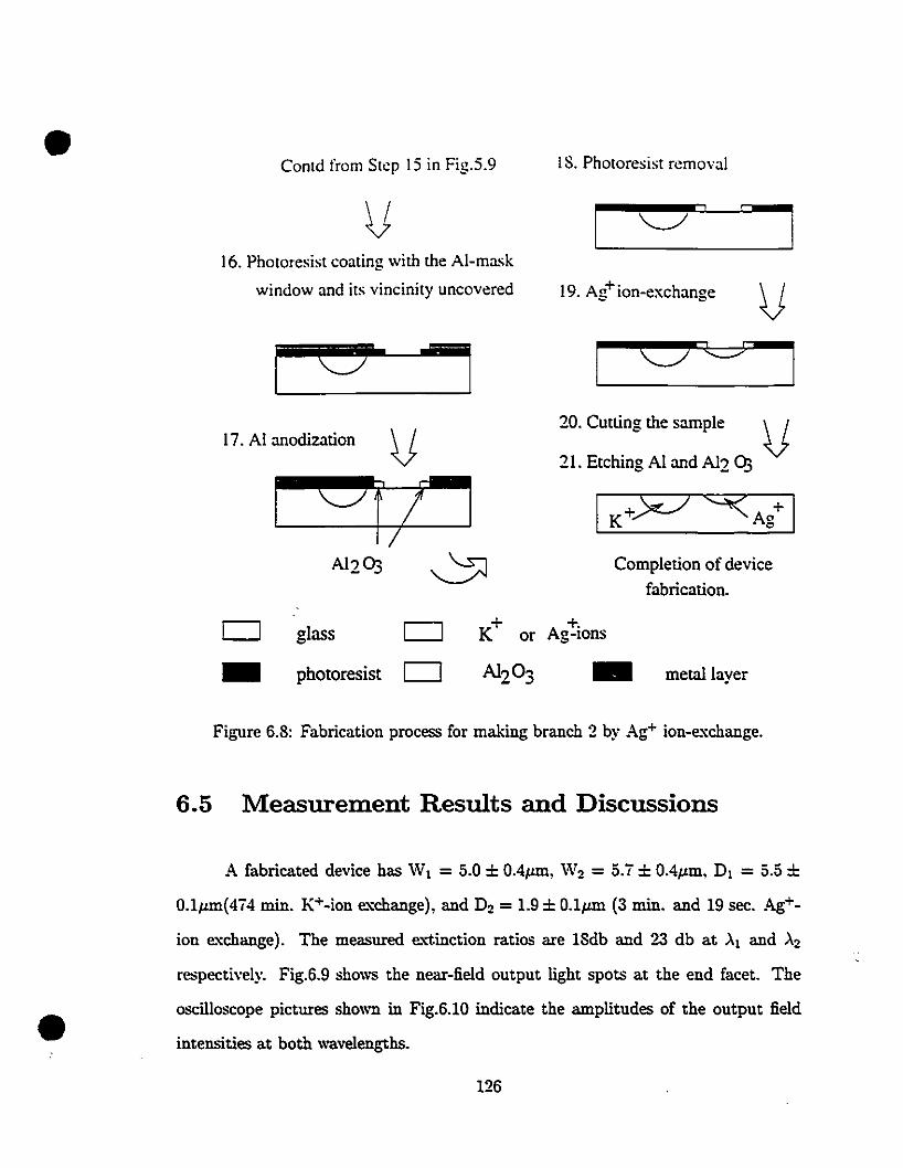
• Conld from Step 15 in Fig.5.9
v16. Pholoresisl coating with the AI-mask
window and ils vincinily uncovered
a
18. Pholoresisl removal
o19. Ag+ion-exchange V
OLJI17. AI anodization V
20. Cutting the sarnple
21. Elching AI and Al2 Q3 v
Completion of device
fabrication.
o
-glass 0
photoresist 0
+ +.K or Ag-Ions
metai layer
•
Figure 6.8: Fabrication process for making branch 2 by Ag+ ion-e:'l:change.
6.S Measurement Results and Discussions
A fabricated device has W l = 5.0 ± 0.4~, W2 = 5.i ± 0.4~, Dl = 5.5 ±
O.1~(4i4 min. K+-ion e."I:change), and D2 = 1.9 ± O.l~ (3 min. and 19 sec. Ag+.
ion exchange). The measured e.'\.1;inction ratios are 18db and 23 db at ..\1 and ..\2
respL'CtÎ\·ely. Fig.6.9 shows the near-field output light spots at the end facet. The
oscilloscope pictures shown in Fig.6.10 indicate the amplitudes of the output field
intensities at both waveiengths.
126
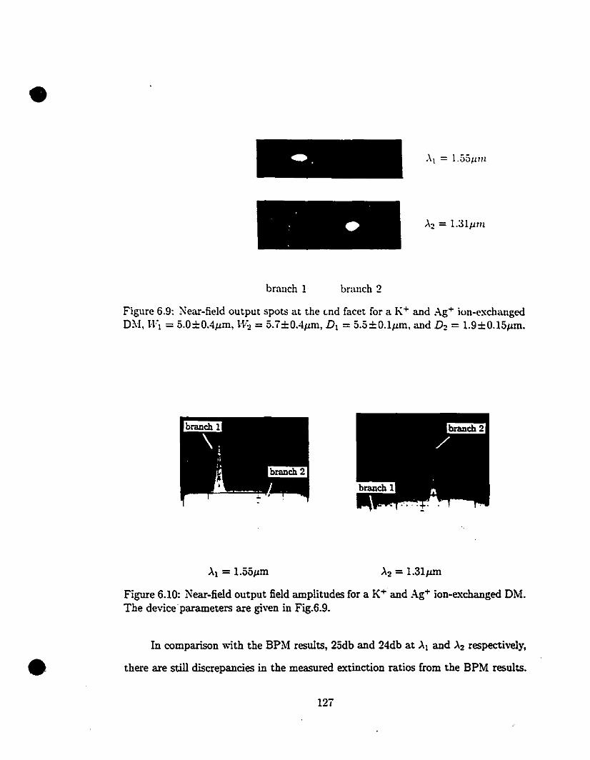
•
• •
brallch 1 brallch 2
Figure 6.9: Near-field output spots at the lnd facet for a K+ and Ag+ ion-exchullged0)'1, H'I = 5.0±0.4J.Lm, lV2 = 5.ï±OAJ.Lm, DI = 5.5±0.1J.Lm, and D2 = 1.9±0.15J.Lm.
•Figure 6.10: Near-field output field amplitudes for a K+ and Ag+ ion-exchanged DM.The device:parameters are given in Fig.6.9.
In comparison \\;th the BPM results, 25db and 24db at >'1 and >'2 respectively,
there are still discrepancies in the measured extinction ratios from the BPM results.
12ï
•
•
•
\VI' b('!ieve that the discrepancies may be main!y due to the width uncertainty and
Ag--ion exchanged depth uncertaint~·. The waveguide widths were obtained by mea
stiring the waveguide mask window widths before ion-exchange. The measurement
rnethod (slot diffration pattern measurement see S~ction 5.4) yielded about ±O.4jl
uncertainty. The Ag+ ion-exchange depth uncertainty might have been caused by the
error in controlling the diffusion time and in the diffusion coefficient From our exper
imental characterization [4J where it is mostly based on the data from multi-mode
waveguides. In addition, the device index structure used in the BPM simulations \Vas
idealized. The side diffusions of both K+- and Ag+-ions, photomask mis-alignment,
non-uniformity of waveguide widths, and so on have ail been neglected in the calcu
lations. These may be the reasons that the e.'l:tinction ratios obtained by BPM are
higher than those measured.
There are several ways to improve the de~ice. First, a smaIler branch angle, for
e.'l:ample (J = 0.003, can be used to increase the ER vaIues as we have discussed in
Chapter 5. Secondly, an increase of the surface inde.'I: change by Ag+ ion-exchange,
for e.'l:ample ~n. = 0.06, may help to enhance the branch asymmetry, and, therefore,
the ER vaIues. The drawback lies in the reduced fabication tolerance. In a future
design, the side-diffusions of both K+ and Ag+ ions should be considered for more
accurate modelling.
lu summary, Ag+ ion-e.'l:changed wa~-eguides have been successfully made af
ter the Al-masks were anodized. The experiment results show that the device by a
two-step ion-e.'l:change process is feasible and can provide high ER values. The re
sults presented are still preliminary. There are severaI ways to Îlnprove the de~;ce
performances which merit further investigation.
128
•
•
•
Bibliography
:1: G. Stewart and P.J.R. Laybourn, "Fabrication of ion-cxchanged llptical \\';wcg-
nidt's froIll dilute silver nitrate melts'·. IEEE .1. Qnantnlll Elec., \·IlI.QE-l-1.
pp.9:30-9:3-l, 19,8.
[2) G. Stewart. C.A. Millar. P.J.R. Laybourn, C.D.\\'. Wilkinson, and R.l\L De
lame. "Planar optical waveguides formed by silver-ion migration in glass". IEEE
.1. Qnantnm Elec.. voI.QE-13, pp.192-20ù, 19".
[:3j G.E. Rindone and \Y.A. Weyl. "Giasses as electrolytes in ga!vanic cells: silver
glasses", .1. Amer. Ceram. Soc., vol. 33, pp. 91-95, (1950).
[-1) F. Xiang, K.H. Chen, and G.L. Yip, "The application of an improved WKB
method to the characterization of diluted silver ion-exchanged glass waveguides
in the near infrared", SPIE conference proceedings, \'01.1 ï94, pp.40-47, 1992.
[5] G. Chartier, P. Collier, A. Guez, P. Jaussaud, and Y. Won, "Graded-index sur
face or buried waveguides by ion e.'Cchange in glass", Appl. Opt., vol. l!), No. i,
pp.l092-1095, April 1980.
[6] G. Chartier, P.J.R. Layboum, and A. Girod, "Masking process for double-ion
exchanged glass optical w1lveguides", Elecron., Lett.. vo1.22, pp.925-926, 1986.
[7] R.G. Walker, C.D.W. Wilkinson, and .T.A.H. Wilkinson," Integrated optical·
waveguiding structures made by silver ion-e.'Cchange in glass. 1: The propagation
129
•
•
•
dlar:u:tcristics of stripc ion-exchangcd \\"a\"cguidcs: a theorctical and experimen
tal im·cstigation··. Appl. Opt.. \"01.22. :\0.12. pp. 1923-1928. (1983).
,.~j S. \\'(~rnick and R. Pinn(~r. Surface Tl'ca.tment of Aluminum, \"oU. Robert Draper.
Lr.d .. Tl'cldington. C.!\: .. 1972.
130
•
•
•
Chapter 7
ProposaIs and Designs:Mach-Zehnder Wavelength DMs
7.1 Introduction
Although a two-ion exchange Y-branch WDM simplifies the fabrication process
for a strip loaded one, it still requires two masks and many fabrication steps to fabri-
cate. )'·lany other structures can be used to form a wavelellgth demultiplexer(WDM),
surit as a X-branch [1]-[2] and directional coupler [3]. Only one mask will be needed
for these devices and their fabrication processes are muc:h simpler. However, their
required lengths are greater and fabrication tolerances low. Recently, it has been
reported that a Mach-Zehnder interferometer [4] cao be used to form a WDM with
high extinction ratios and less sensitivity to fabrication parameters. The device also
requires only one photomask for fabrication.
Fig.ï.1 shows the configuration of a Mach-Zehnder interferometer DM. lt con
sists of a 3-db power divider which splits the input power into two int.erferometer
arms. A 4-port hybrid coupler, formed by a syrnmetric converging section (a 3-db
combiner) and an asyrnmetric Y-branch mode splitter, is located at the end of the
interferometer. The two arms of the interferometer are designed to be asymmetric
such that a phase delay will be realized in one arm at the end. Conventionally, one
131
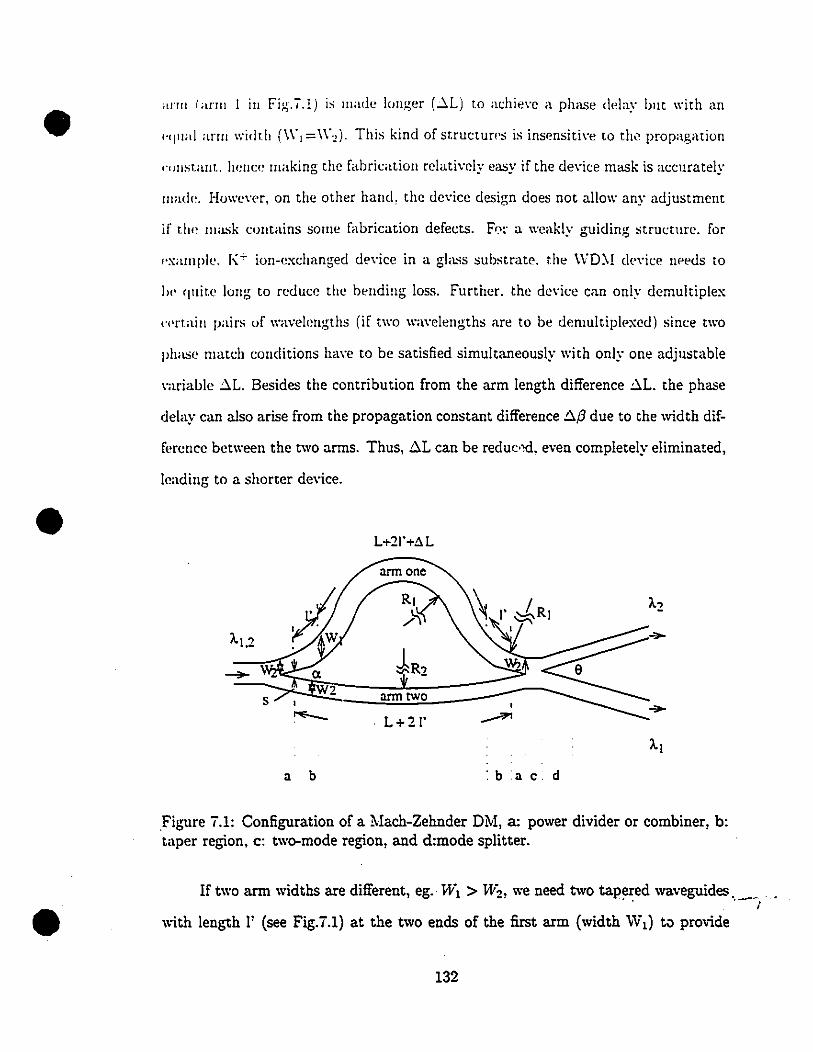
•
•
;lI'm (al'fn 1 in Fi~.ï.l) is made l()n~er (~L) to achie\'e a phase dela" bm with an
(''Illai al'In widr.h (\\"=\\"1)' This kind ofstructun's is insensitive ta tl", propagation
l'fJllstanr.. henc!' making the fabrication relatively cas" if the de\'ice mask is accurately
malk Huwe\'er, on the other haIlli, the de\'ice design does not allow any adjustment
if d", mask contains some fabrication defects. Fn:' a weakly guiding structure. for
l'xample. r;:~ iun-exchanged de\'ice in a g};L~S substrate. the \VD:\! de\'ice npeds ra
1,,· '1nite long to reduce the bending 10ss. Further. the device l'an onl" demultiplex
("'nain pairs of wavellmgths (if two w,n-elengths are to be demultiplpxed) since two
l'ln,,' match conditions lu\\'e to be satisfied simultaneously with only one adjustable
mriable ~L. Besides the contribution from the arm length difference ~L. the phase
delay l'an aIso arise from the propagation constant difference .6.13 due to the width dif-
ferenec between the two arms. Thus, .6.L l'an be reduc'~d. l'ven completely eliminated,
leading to a shorter device.
L+21'+~L
s
a b
arm one
ann two
L+21'
: bac. d
•Figure ï.1: Configuration of a Mach-Zehnder DM, a: power divider or combiner, b:taper region, c: two-mode region, and d:mode splitter.
If two arm \\;dths are different, eg.· vITI> "''2, we need two tap~ed waveguides .. __ .1
with length l' (sel' Fig.ï.1) at the two ends of the fust arm (width W I ) t() provide
132
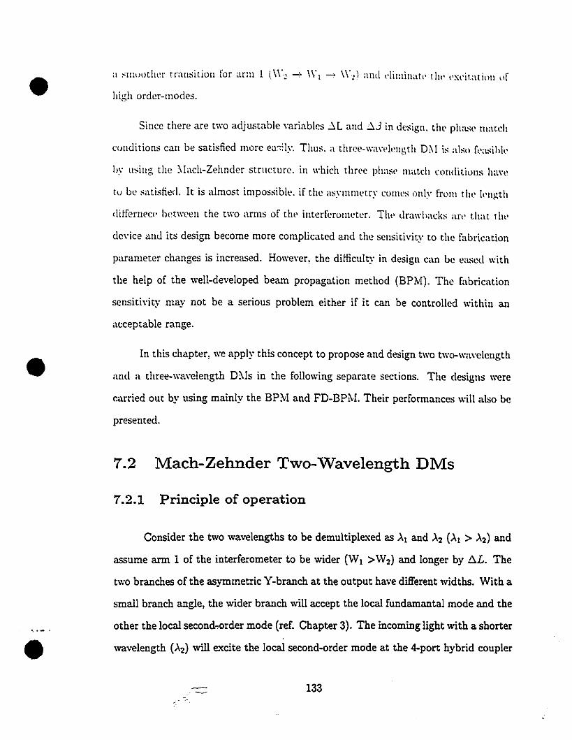
•
•
~ .- .
•
high order-modes.
Since there are two adjustable \"ariables ~L and ~3 in design. the pha.'e match
conditions call be satisfied more eac:ly. Thus. a three-w,weI''Ilgth DilI is aIs" f",,-'ihl,'
hy IlSillg the :-Iach-Zehnder structure. in which three phase match conditions ha\"!'
to be satisfied. It is almost impossible. if the aS\'mnletn' CllnleS onh' l'mm the h'nulh. . . "ditfernece Iwt\\"eell the t\\"o arms of thl' interfl'rometer. The drawbacks an' that th,'
de\'ice and its design become more complicated and the sensiti\"ity to the fabrication
parameter changes is increased. Howe\"er, the ditficulty in design l'an be ",,-'et! with
the help of the well-developed beam propagation method (BPM). The fabrication
sensiti\"ity may not be a serious problem either if it l'an be controlled within an
acceptable range.
In this chapter, \\"e apply this concept to propose and design two t\\"0-\\"a\"elength
ant! il three-\\"a\"elength D:\ls in the following separate sections. The designs \\"cre
carried out by using mainly the BPM and FD-BPM. Their performances will also be
presented.
7.2 Mach-Zehnder Two-Wavelength DMs
7.2.1 Principle of operation
Consider the two wavelengths to be demultiple.xed as >'1 and >'2 (>'1 > >'2) and
assume arm 1 of the interferometer to be ,vider (W1 >W2) and longer by t:.L. The
two branches of the asymmetric Y-branch at the output have different widths. With a
small branch angle, the ,vider branch will accept the local fundamantal mode and the
other the local second,order mode (ref. Chapter 3). The incoming light with a shorter
wavelength (>'2) will excite the local second-order mode at the 4-port hybrid coupler
133
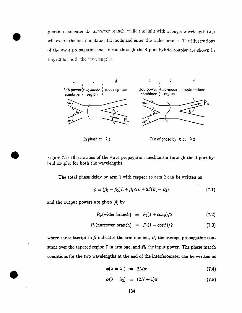
• .J"11C'Ii"n and "ntl'r the narrower brandl. while the light with a longer wavelength (,\d
will excik the local fundarn('ntal mode and enter the wicler branch. The illustrations
,,1' 1.1", wave propagation machinislTl through the 4-port hybrid coupler are shown in
fil!, .•.2 for both the wavelengths.
da C1l ,
3db power 1two-mode ,combiner 1 region 1
d
mode splitter
a c,,3db power 'two-modecombin~r 1 region
1,1 mode splitter1
Figure •.2: Illustrations of the wave propagation mechanism through the 4-port hybrid coupler for both the wa\·elengths.•
In phase at À. 1 Out of phase by lt at À.2
where the subscript in .8 indicates the arm number, ilt the average propagation con
stant over the tapered region l' in arm one, and Po the input power. The phase match
conditions for the two wavelengths at the end of the interferometer can be \Vritten as
•
The total phase delay by arm 1 with respect to arm 2 can be written as
t/! = (.81 - fh.)L + .81!1L + 2['(.81 - fh.)
and the output pO\vers are given [4] by
P.,(wider branch) - Po(1 + cos<jJ)/2
Pn(narrower branch) - Po(1 - costf;)/2
t/!(>. = >'1) - 21\11l'
t/!(>' = >'2) - (2N + 1)1l'
134
(i.l)
(i.2)
(i.3)
(i.4)
(i.5)
•
•
wlH'n' .H ::; .Y aud JI . .\" = 1.:2..... Thus. ar rlll' "hortl'r wa\"t'Il'u~rh .\~ (Sl'l' E'Is.(7.1)
auti (7.5)). siucc rhc lighrs with l'quaI pOWl'r l'rom rh,' rwo illfl'rfl'roml'l,'r anlls ar,'
Dur of phase !Jy IS00 at the Olltpllt l'ud. a Sl'coud-onkr IllOti,' will Lw l'xrirl'd iu rh,'
jllucrion waVl'guidl' of the -l-port hybrid coupler. ..I,t the longer wawlt'ngth '\1' sinn'
rhl'\' are iu phast' (sec Eqs.(7.11 and (7..1)), a fund.ullentalIllotil' will 1", l'Xl'itl'd. !l eau
Ill' dearly Sl'l'U iu Eq.(7.1) thar the total phase tielay l'an Illainly arisl' froIlll'irh,'r the
\\':\\'(;':;l1ide propag:~tion contitant ditft~renl't:' lwt\\'CPIl thl' twu anus. ~i\"('11 hy t.he nr:-;t
rl'nn of Eq.(7.1) or the arm length diff'crence in tht' second tl'rIll sinn' th,' rhinl tenn
is \'l'r,' sIllal1. [1' the two al'lns are idl'ntieal in witith. !Joth the fit'sr and thinl t,'rIll
mnish. yie[ding the de\'ice reported in Hl. Another limit is to set ..J.L to zero so that
the phase delay will ail come from the difference in {J. Since the error iu the phase
delay caused by the l'l'l'or in the propagation constants is approximately proportiona!
to L (sec Eq.(ï.l)), L shou!d be kept short to l'l'duce fabrication sensiti\'ities of the
----- N-M=ON-M=l
~-T\----~ -
~ -" .,,,,,,,,,,.'
•Figure 7.3: Light power from the \vider branch versus light wavelength.
When the wavelength >. increases from >'2 to >'1> the output power P", (sec
135
•
•
•
E'I.17.:.!)) will ~u rhruugh 21S - .\1) -;- l time uscillations bet\\"l'pn zero and Po IL,
,h'''\"I1 in Fig.7.3. The salIW conclusion c:J.n also be drawn on P". Therefore, to
lJ"tain l.he widest bandwidth possible, ?\[ and N should be chosen equ:J.I for only one
lJscillatiun bet\\'t'en '\1 and ,\~ (the dashed [ine in Fig.i.3). :\.s we can see in the phase
ilia 1.<'1 1 Ct>llditiuns. a small phase delay gcnerally requircs a short L. ?\[ and :\ should
ais" Ill' kept small 1.0 recluce fabrication sensiti"ities of the de"ice.
Fur a d''''in' with an identical arrn width. there is one \'ariable '::"L and t\\'o
integ..r "ariables ?\l and :\ in t\\'o phase match condit:.lliS Eqs.(iA) and (i.5). Only
certain pairs of wavclengths Al and A2 can satisfy the two phase match conditions
simultancously. However, if the difference in the propagation constants bet\\'een the
two anus also contributes to the phase delay, {3t (Wr.), .th ('W2 ) , and Lare tte
additional "ariables adjustable to satisfy the two phase match conditions. Thus, the
\\'avelcngths to be demultiplexed can be chosen more freely in this de\·ice.
7.2.2 Deviees and their performances
The first device has both its arms equal in length, !lL = 0, as a special
example. The second de\'ice has a phase delay in arm 1 due to both !:lL and !lf3.
üsually, symmetric Y-branches are needed at both the beginning (first) and the end
(second) of the Mach-Zehnder interferometer as shown in Fig.ï.1, which act as a 3db
power devider and a 3db power combiner, respectively. It is understandable that,
between the two output branches of a Y-branch, one receives more power if its width
is wider but less power if it is bent. outward with larger angle. In device two, by
balancing the bending (i.e. adjusting Rt ) and widening {adjusting l') of the branches
counected to arm l, we can design to have an equal power output from the two
branches at a distance l' away from the fust Y-branch ape.'I: and hence also an equal
power input into the two branches at the second Y-branch ape.'I:. In other words, the
136
•
•
•
taper regions (region b in Fig.'.I) function not only as adiabatic transition (W~ --+
\Yl --+ \Y~) but also a 3db di\'ider and a 3db combiner (region a in Fig.i.I). Thus. the
symmetric Y-branches (region a) are not needed (s=O) and the ll'ngth of the de\'iel'
l'an be shortened.
To achieve the difference in 13. we hm'e chosen different widths for the two
arms but kept their depths l'quai for single-step fabrication. By choosing differem
values of ~L,L,WbW2,and waveguide depth D in Eqs.('.I), (i.4), and (i.5). wc l'an
have many combinations of solutions. The parameters should be chosen to meet the
requirements for small M and N values, a shorter device, small bending loss, being
away from mode cutoffs, low sensitivity to parameter variations, and so on.
AI = 1.55 and A2 = 1.31 have been chosen to be the two wavelengths to be
demultiple.'Ced. The waveguide structure used for testing the device concept is to be
made by K+-Na+ ion-e.'Cchange in a soda-lime glass suhstrate at temperature T=385°
[5] and [6]. The inde.'C profile in the depth direction is Guassian-Iike with 0.01 as the
ma'Cimum inde.'C change on the waveguide surface for both wavelengths. nb=1.50n
and 1.4982 have been taken as the glass indices at wavelength A2 and Ait respectively.
Any side diffusion in the fabrication process has been neglected in the design. The
designs were performed for the TM polarization with respect to the waveguide surface.
The depths of K+ ion-e.'Cchanged waveguides are given by the effective depths defined
in Chapter 4.
For the first device, an ion-exchange depth D=4.5Ilm (ion-exchange time t = 284
min.), WI=8.2Ilm, \V2=4.0Ilm, ~L=O, L=2430.0Ilm, the branch separation at the
end (or the beginning) of symmetric Y-branch power divider (or combiner) s=17.5/lll1,
M=N=l, the waveguide bending radius R=64.7143mm for both arms were chosen,
and the caIculated extinction ratios are 34.41db at AI and 31.56db at >'2, respec
tively. For the second device, D=5.5/lll1 (t = 341 min.), W1=10.09Ilm. W2=3.8/lll1•
137
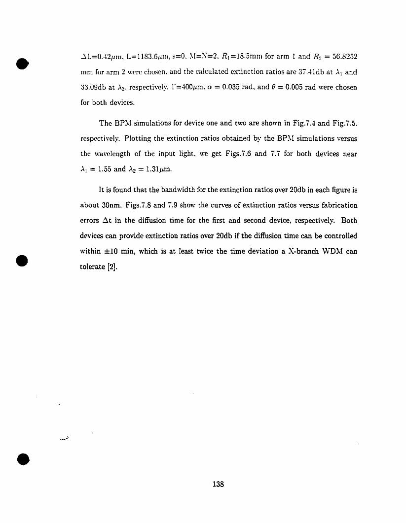
•
•
•
~L=U.·12/lm. L=1183.6jWl, s=O. ~1=~=2. R I =18.5mm for arm 1 and R2 = 56.8252
mm fur arln 2 wcre chusen. and the calculated extinction ratios are 3ïAldb at ..\1 and
33.09db at "\2, respectivcly. 1'=.JOO/lm, Q = 0.035 rad. and () = 0.005 rad were chosen
for both devices.
The BPM simulations for device one and two are shown in Fig.ïA and Fig.ï.5.
respectÏ\·ely. Plotting the extinction ratios obtained by the BPl\I simulations versus
the wavelength of the input light, we get Figs. ï.6 and i.ï for both devices near
lt is found that the bandwidth for the extinction ratios over 20db in each figure is
about 30nm. Figs.ï.8 and ï.9 show the cun.·es of extinction ratios versus fabrication
errors ~t in the diffusion time for the first and second device, respectively. Both
devices can provide e."<tinction ratios over 20db if the diffusion time can be controlled
within ±10 min, which is at least twice the time deviation a X-branch WDM can
tolerate [2J .
138
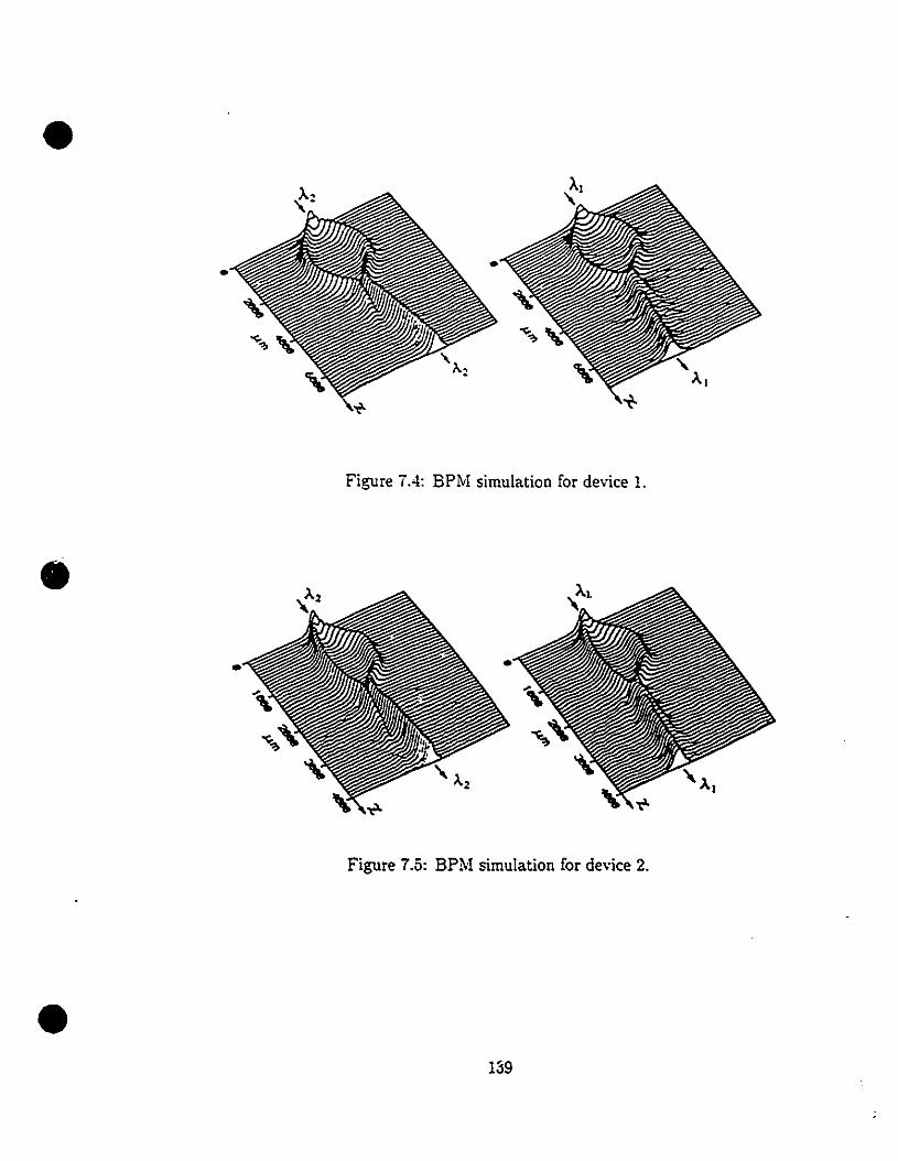
••
Figure ï.4: BPM simulation for device 1.
•
•
•
Figure ï.5: BPM simulation for device 2.
139
•40- - device one ..
.0 ."tl
30.... device two
'-'
0:;:;0...c: 200
:;:;uc: 10:;:;x
lLJ
0
• 1.45 1.50 1.55 1.60 1.65
Àl CJ.un)
Figure Î.6: Curves of extinction ratio vers<ls the input wavelength >'1 for both devices.
40 ...- - device one.0"tl
30.... device two
'-'0
:;:;0...c: 200
• :;;Uc: 10:;:;x
lLJ
01.20 1.25 1.30 1.35 1.40
À2 ~m)
Figure Î. Î: Curves of e.xtinction ratio versus the input wavelength >'2 for both de\ices.
•140
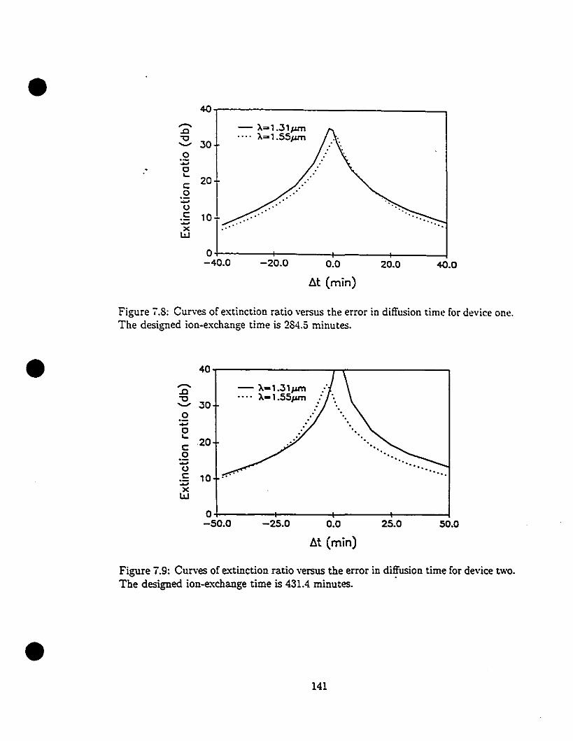
• 40- - À~1.31JU'loC
" 30. . .. À~1.SSJU'l
'-'
0:;:;0...c: 200
:;:;0c: 10~
xW
0-40.0 -20.0 0.0 20.0
~t (min)40.0
Figure 7.8: Curves of extinction ratio versus the error in diffusion time for device one.The designed ion-exchange time is 284.5 minutes.
• 40
- - À=1.31~oC
" 30À-l.SS~
'-'0
:;:;0...
20c:0
:;:;0c: 10 .'
:;:;x
W
0-SO.O -2S.0 0.0 25.0
~t (min)
50.0
•
Figure 7.9: Curves of e;'<tinction ratio versus the error in diffusion time for device two.The designed ion-e.'Cchange time is 431.4 minutes. .
141
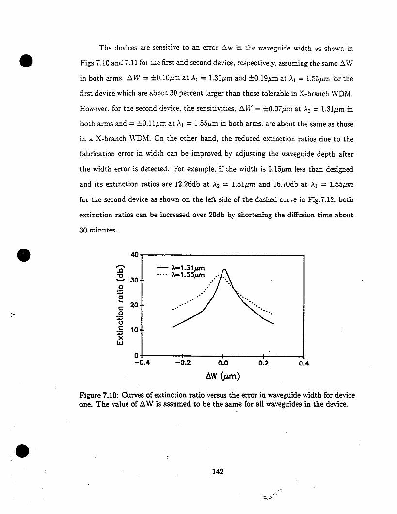
•The dcvices are sensitive to an error ~w in the wa\'eguide width as shown in
Figs. ï.lO and ï.ll fOl t;.~ !irst and second device, respectively, assuming the same ~W
in both arms. ~W = ±O.lO/Lm at >'1 = 1.3l/Lm and ±0.19/Lm at >'1 = 1.55/Lm for the
!irst device which are about 30 percent larger than those tolerable in X-branch \VDM.
Howcver, for the second de\'ice, the sensithities, ~W = ±O.Oï/Lm at >'2 = 1.3l/Lm in
both arms and = ±O.ll/Lm at >'1 = 1.55/Lm in both arms. are about the same as those
in a X-branch WDM. On the other hand, the reduced extinction ratios due to the
fabrication error in width can be improved by adjusting the waveguide depth after
the width error is detected. For example, if the width is 0.15/Lm less than designed
and its extinction ratios are l2.26db at >'2 = 1.3l/Lm and 16.ïOdb at >'1 = 1.55/Lm
for the second device as shown on the left side of the dashed curve in Fig.ï.12, both
extinction ratios can be increased over 20db by shortening the diffusion time about
30 minutes.
• 40....... - >'=1.311UT\oC-0
30>'''1.551UT\....,
0:;;0 ..'- 20c:
:. 0 ".:;;CJc: 10.-....X
IJJ
0.40.20+-----+----+----+------1-0.4 -0.2 0.0
âW CJ,l.m)
Figure ï.lO: Curves of extinction ratio versus the error in waveguide .....idth for deviceone. The value of ~W is assumed to be the same for all waveguides in the di:!vice.
•142
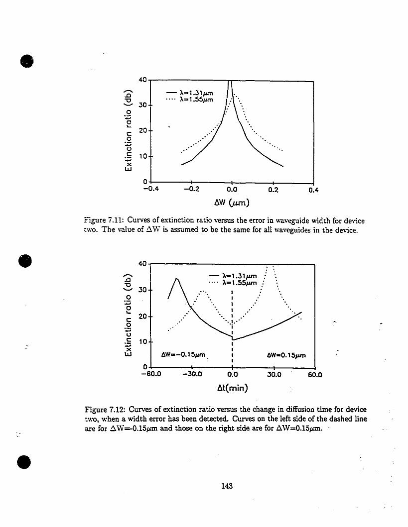
• 40
........ - À~1.31J'lTl.Q .-c
30.. .. À~1.55J'lTl
-....-0~0L-
e: 20
.2~
0e: 10~x
W
0-0.4 -0.2 0.0 0.2 0.4
bW (um)
Figure 7.11: Curves of e.xtinction ratio versus the error in waveguide width for devicetwo. The value of !J.vii ho assumed to be the same for ail waveguides in the device.
40r------------=--:-----,
: ",
..
- ~1:Il.J1JUT1 .À~1.SSJUT'
." .
20
10
30
• ..........a-c-....-0~
0L-
e:.2~
ue:- ~- x
W
60.030.0-30.00+----+---4----1----1-60.0
•Figure 7.12: Curves of extinction ratio versus the change in diffusion time for devicetwo, when a width error has been detected. Curves on the left side of the dashed Hneare for !J.W=-O.15~m and those on the right side are for IlW=O.15~m. '
143
• Si'.lIilar .."sIlIts have abo bCf'll obtaineu for the first de\·ice. 1 i:e ue\'ices are also
t.!'su"l h\' BP:-'I simulations for the TE polarization with lower ER's. anu found to be
polarizatioll depelldellt uue ta the birefringellce of the K- ion-exchanged waveguide
ill a giass sU!Jstrate. The optirnization for TE operation should be pursued separatel::.
~?3,._. Discussions
•
•
A.s pr"sellteu ill rhe previuus subsectioll. the workillg lellgths L (L+1' to be
III(JI'" precise) uf w:weguicle which contribme ta the pha,;e delay ill arm Olle are 2-130
111Il anu 118-1 Jlrn in the first and second device, respectit·ei::. In cornparison with that
in a X-branch \\'0)'-1, it is shorter, especially in the second one. A shorter L together
with small M and N values (M.N=4-6 in a X-branch WOM [2]) in Eqs.(ï.4) and
(ï.5) are the reasons wh:: the de\'ices reported here have less fabrication sensitivities,
The wiclth sensiti\'it:: of the second device ':tas not been improved over that of a
X-hralldl \\'0:-'1 because the narrowed wm'eguide width of al'm two increases the
,('n,iti\'it:: and weighs against the impro\'ement due to a shorter L and sIllall :-'1 and
X, The fabrication sensitivities in both the width and depth can be further reduced
by increasing the phase delay contribution from t;;.L in branch 1 \Ihich, however, will
increase the device length. If the separation of the output branches is assumed to be
lOilm, the totallengths of the second device presented here, an X-branch WOM [2],
and a :\1-2 \-YOM without the difference in f3 between its two arms are about 4mm,
ïmm, and ïmm. The new device is almost half of the others in length. Our second
de\'ice can be further shortened by reducing the width of the second arm if the width
sensith;ty is not a problem.
144
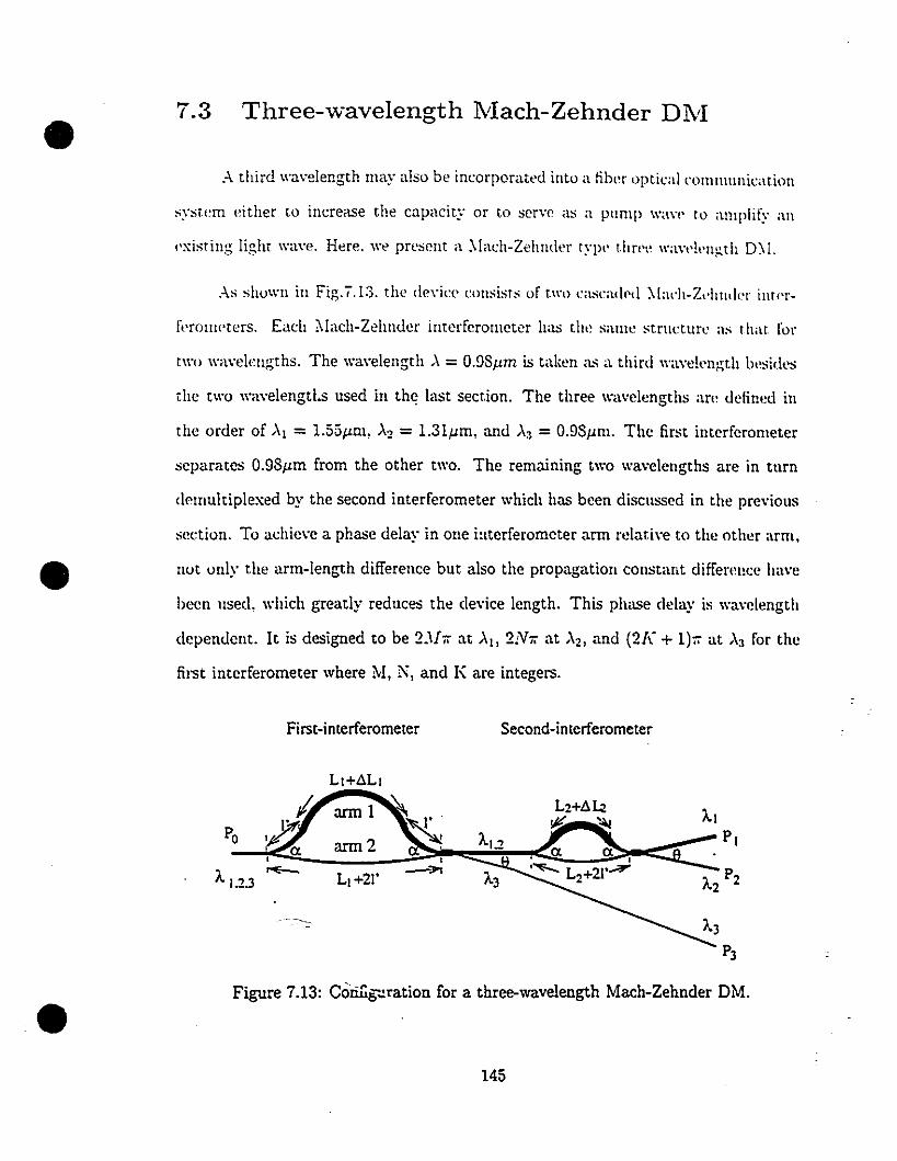
• 7.3 Three-wavelength IVIach-Zehnder DIVI
.-\ third wavelength IIla}" aisa be incorporated into a liber npticaI l'Ollllllllllication
•
'YSI.em "ither tn increase the capacity or to serve as a pllIllp waw ta amplify an
,'xi'ling Iight ,,",1\·e. Here. we presem a :\Iach-Zehnder ryp" thn'e wawlt'nf!,th D~I.
l..-rollleters. Each )'Iach-Zehndcr imerferollleter has the same stmeture as 1hal for
two wavelcngths. The wa\'elength .\ = O.9SJLm is taken as a thin! wavell'np;th bcsides
the two wavelengtl.s used in th~ last section. The three wavelengths are delined in
the order of Al = 1.55JLIIl, A2 = 1.31JLm, and A3 =O.9SJLIIl. The first illterferometer
separates O.9SJLm from the other two. The remaining two wavelengths are in tnm
clemultiplexed by the second interferometer which has been discnssed in the previons
section. To achie\'c a phase delay in one interferometer arm rclati\'e to the other arm,
not only the arm-length difference but also the propagation constant difference hm'e
been nsed, which greatly reduces the device Icngth. This phase delay is wavelength
dcpendellt. It is designed to be 2Jh at Ah 2N.. at '\2, and (21( + 1).. at '\3 for the
first interferometer where M, N, and K are integers.
First-interferometer
Ll+IlLl
Second-interferometer
•
A 1.2.3
----~
Figure 7.13: Conug;.:.ration for a three-wavelength Mach-Zehnder DM.
145
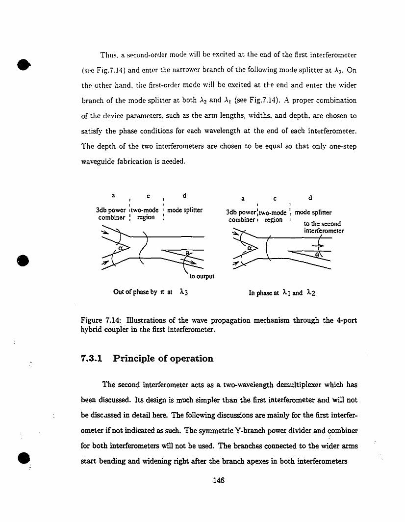
• Thus. a spcond-order mode will be exci~ed at the end of the first interferometer
(sec Fig.ï.14) and enter the narrower branch of the following mode splitter at À3 • On
the other hand. the first-order mode will be excited at tre end and enter the wider
branch of the mode splitter at bath À2 and À I (see Fig.ï.14). A proper combination
of the device parameters, such as the arm lengths, widths, and depth, are chosen ta
satisfy the phase conditions for each wavelength at the end of each int~rferometer.
The depth of the two interferometers are chosen to be equal so that on!y one-step
waveguide fabrication is needed.
•
a c,,3db power ,two-modecombiner: region
d,1
, mode splitter,
to output
a c, ,3 ' 1db power, two-mode ,combiner 1 region ,
d
mode splitter
to the secondinterferometer
Out of phase by 1t at À.3 In phase at À. 1 and À.2
•
Figure 7.14: Illustrations of the wave propagation mechanism through the 4-porthybrid couplèr in the first interferometer.
7.3.1 Principle of operation
The second interferometer acts as a two-wavelength demultiple:'(er which has
been discussed. Its design is much simpler than the first interferometer and will not
be disc.lSSed in detail here. The follcwing discussions are mainly for the first interfer
ometer if not indicated as such. The symmetric Y-branch power divider and combiner
for both interferometers will not be used. The branches connected to the wider arms
start bending and widening right after the branch apexes in both interferometers
146

( .• As ~hown in Fig.ï.13 for tlH' fir~t Îllterferollle[er. th,'n' an' two tapert'd W"\'l'g
uide with a !ength rat the two ends of the fir~t arlll which han' tlll' ~alll(' funl"tion a.,
wc had pointed out for the two-wavelength O"I. lu [his work, l' = ·IOO/11ll i~ dlll~en
for bath interferometers. Assume arm 1 ta be wider (11"11 > 11"1::, where the lir~t
subscript indicates the arder of the interferometer and the ~econd is for the order
of the interferometer arm) and longer by ~Ll than arm 2. The total rt'!atÏ\'e phase
delay in urm 1 ccmpared with arm 2 can be written as
where i indicates the order of the wavelength. The output powers l'an still be expressed
by Eqs.(ï.2) and (ï.3). The phase match conditions for the three wavelengths al. the
end of the first interferometer are given by
<1>(>' = >'1) = 2M..
<1>( >. = >'2) - 2N,.
q,(>. = >'3) - (2K + 1)11"
(j.ï)
(ï.8)
(ï.9)
•
where M < N :5 K and M, N, K = 1,2" ". Thus, at the shortest wavelength >'3 (sel'
Eqs.(ï.6) and (ï.9), since the lights with l'quai power from the two interferometer
arms are out of phase by 180· at the end of the interferometer, a second-order mode
will be excited in the junction waveguide of the 4-port hybrid coupler (sec Fig.ï.14).
At the other wavelengths >'1 and >'2, since they are in phase (sec Eqs.(7.6), (7.7),
and (ï.8)), a fundamental mode will be excited. LI should be kept short to l'l'duce
fabrication sensitivities of the device. Eliminating LI and oC1LI in the three phase
conditions together \vith Eq.(7.6) we have a nonlinear equation given by [Appendix
ï.4.1)
147
•
•
•
n1lN)..2 - 21'nll(Ti2ï - n22) - n2IA'!)..1 + 21'n21(TrjJ - n12)nll(n21 - n22) - n21(nll - n12)
_ nll (K + 1/2)..3 - 21'nll (TiJï - nd - n31 A!)..1 + 21'n31 (TrjJ - n12) = 0 (i.10)nll (n31 - n32) - n31 (nll - n12)
where ni) indicates the arm j's effective index ({3i)2rr/ )..i) at the i th wavelength. The
adjustable parameters in Eq.(i.10) are WIl , W12 , the waveguide depth D, M, N, and
K. The values of M, N, and K are restricted by M < N ::; K for the reason of
)..3 < )..2 < )..1 and are required to be small for a reasonable device length. AIso, some
combinations of M, N, and K are beyond the possibility of satisfying Eq.(7.10). There
are about only 4 or 5 combinations of M, N, and K values for this example that can
be chosen for the design. After M, N, and K are chosen and WIl and W12 are initially
chosen between 3.0Jlm and 10.0Jlm (W12 < WIl)' D can be solved from Eq.(7.10) by
a root-searching technic:ue. DoLI and LI can then be found by Eqs.(7.14) and (7.15).
The solution may not be proper, such as the device being too long, waveguide tao
deep, and so on. New branch widths or the M, N, and K combinations have to be tried
until a proper solution is reached. For this example, M=3, N=4, K=5, LI = 2800Jl,
DoLI = 1.54/lffi, D = 4.7/lffi, WIl = 7.0/lffi and Wl2 = 4.0Jlm.
7.3.2 BPM simulations
The phase delay given in Eq.(7.6) is for straight waveguides. The interferom
eter arms are curved all the way from beginning to the end of each interferometer.
The propagation constant of a straight waveguide is different from that of a curved
waveguide. This will result in phase mismatches at the end of each interferometer
for the three given wavelengths. The performance of the device cau be simulated
by the BPM. The effective index method was used to reduce the three dimensional
problem into two dimensional problem. The device is aIso assumed to be made in a
148
•
•
•
glass substrate by a purely thermal I\~ ion-exchange. Th,' glass indl'x is giwn by
nb=1.5053 at ,\ = 0.9Sllm. Fig.ï.J5 shows a two-dillll'nsional effectivl' index profill' of
the device with the effective waveguide depth 0=.1. j /lm with t=3~6 minutes diffusion
time.
At the beginning, the simulations of two interferometers were donc separately.
The phase mismatches are corrected by changing thl' arm lengths or mm ll'ngth
differences (LI or .:lL I for the first interferometer) until good results (ER;:::25db) for
all three wavelengths are achieved. Thus, the new arm length and length difference of
the first interferometer are LI = 2864.0/lm and .:lLI = 1.52/lm. The bending radius
of the first arm Ru is 2309i. il/lm where the first subscript indicates the order of the
interferometer and the second is for the arm order (sel' Fig.i.l). The bending radius
of the second arm RI2 is 104685.ïljlm.
For the second interferometer, the choscn parameters are 0=4.ijlm, L2 =
1880.0jlm, t:.L2 = 0.90jlm, W21 = 1O.Ojlm, W22 = 5.5jlm, R21 = 19146.14jlm, and
R22 = ï6628.5ijlm. The branch angles Q andO (sel' Fig.i.13) are 0.035 rad and 0.005
rad respectively.
The BPM simulations for the whole device are carriee! out by a more efficient
FO-BPM since the length of the whole device is quite long. The results are shown
in Figs.i.16, i.li, and i.18 for >'1> >'2, and >'3 respectively. The extinction ratios are
given in Table i.l where Pi, i=1,2, or 3, is the power from the device output branch
i as shawn in Fig.i.13. The extinction ratios are relative ta the power out from the
designed output branch. For example, at >'1> the designed output branch is branch 1
and the extinction ratio is given by
ER = 1010910~ , i=l, 2, or 3.
The total lengtb of the device is about 1.5cm wlLicll is relatively shorter than a
directional-coupler version 1.8-2.Ocm in [il. Again, the device for TE polarization has
149
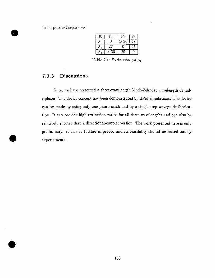
1 A" 1 > 30 1 29 1 0 1
: db 1 Pl 1 P2 1 Pli )'1 1 0 1 > 30 1 28! '\2 1
'r1 0 l'r-, , -v
•Tabl.. ï,l: Extinction ratios
ï.3.3 Discussions
Here, wc have presented a three-wavelength :\Iach-Zchnder wavelcngth demul
tiplexer. The ùc\'ice concept ha~ been demonstrated by BPi\! simulations. The device
can be made by using only one photo-mask and by a single-step waveguide fabrica
tion. It can provide high extinction ratios for all three wavelengths and can also be
•relativcly shorter than a directional-coupler version, The work presented here is only
prelill1illary. It can be further impro\'ed and its feasibility should be tested out by
l'XperiClncnts.
•150
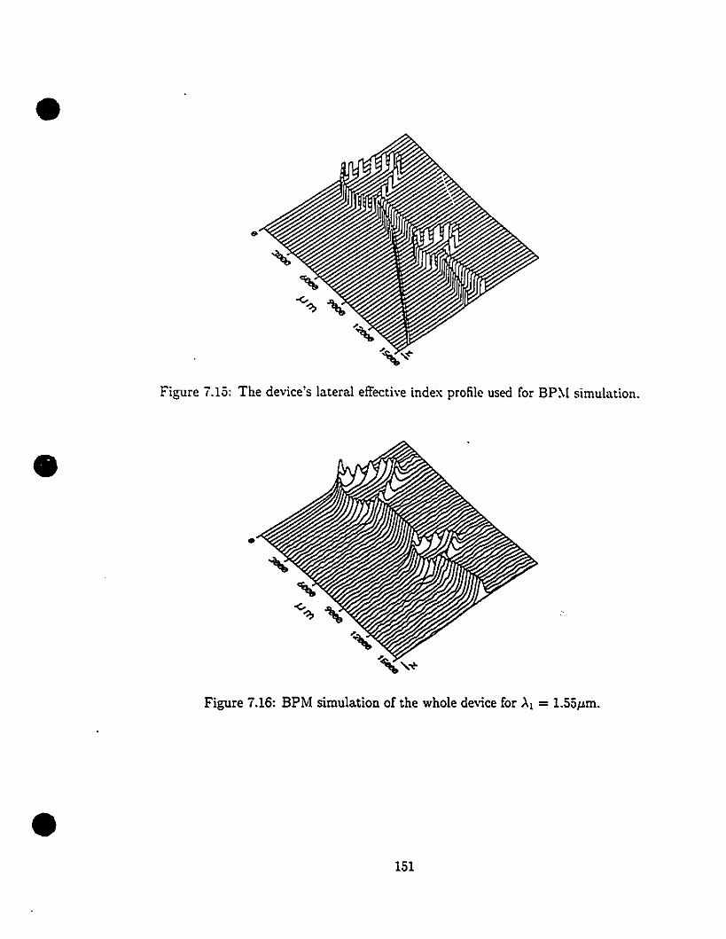
•
Figure ï.15: The device's lateral effective index profile used for BP~( simulation.
••
•
Figure 7.16: BPM simulation of the whole device for '\1 =1.55JLm.
151
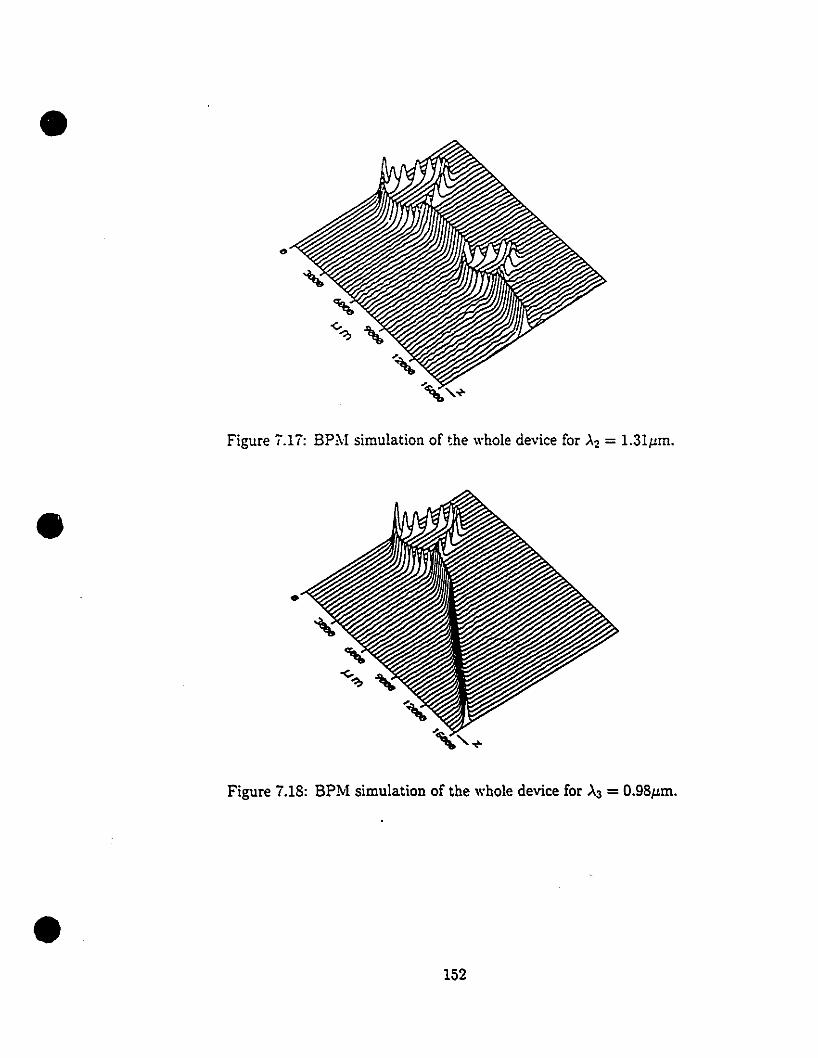
•o
Figure Î.li: BP"! simulation of the whole device for >'2 = 1.31fLm.
••
•
Figure 7.18: BPM simulation of the whole device for >'3 = O.98fLm.
152
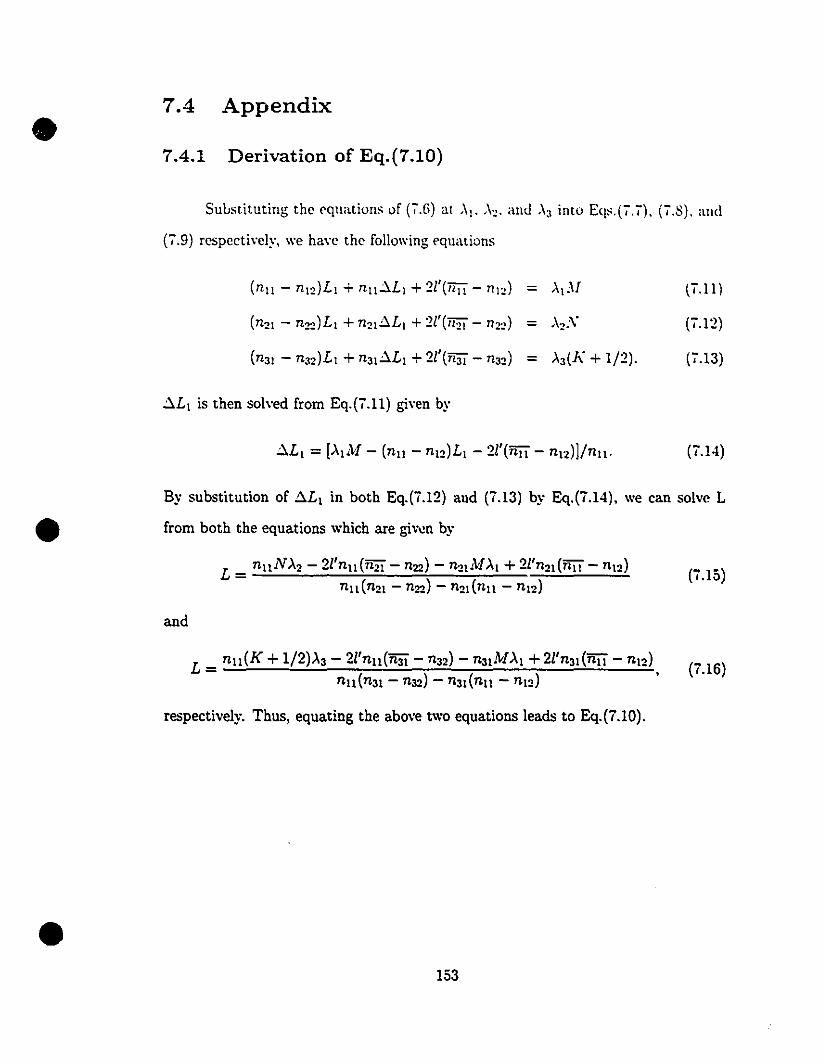
•
•
•
7.4 Appendix
7.4.1 Derivation of Eq.(7.10)
SuLst.ituting the equations of (7.6) al '\1 .•\~. and ,\:< into Eqs.(7.7). (7.S). and
(7.9) respectîvely. we have the following equations
(nll - ndL I + nll~LI + 2/'{üiï - n12) = '\IJ! (7.11)
(n21 - n22)L1+ n21~Ll + 21'(1l~1 - n:d = ,\~S (7.12)
~Ll is then solved from Eq.(i.ll) given by
By substitution of ~LI in both Eq.(7.12) aud (7.13) by Eq.(7.14), we can solve L
from both the equations which are givlln by
L = nllN>"2 - 21'nll (Ti2ï - nd- n2l lv!>"1 + 2l'n21 (Tiiï - n12) (i.15)nll(n21 - n22) - n21(nll - n12)
and
respectively. Thus, equating the above two equations leads to Eq.(7.10) .
153
•
•
•
Bibliography
:1i ,-\, :\","-1". "Gllided-wa\'e dc\'ices based ou two-mode itlterfereuce··. SPIE Pro-
'" , , 1 90" (j'S --" 19~5l'l'f-'( 1I~g.~. \ U. ....J. pp. -1 v. ..;cpr.. \.:.
[:?j G.L. l'ip and L.J. Babin. "BP;"! design ofa widened X-brandI demnltiplexer in a
glass sustrate by K+ iori e.'l:challge for À = 1.31J.lm and À = 1.55J.lm" . IEEE-OSA
Iutegrated Phot.onics Research Proceedings, \'01. 10, pp.72-75, ;"Iarch, 1993.
[3) H,C, Chen:; and RoV. Ramaswamy, "Symmctric directional coupler as <1 w<l\'e
ll·l·":~th ulUltiplexer-demultiplexer: thcory and experiement", IEE!: J. of QUllutum
Electron,. \'01.QE-27, :\0.3. pp.5Gi-57-1. 1991.
[-II A. Ter\"Onen, P. Poyhonen, S. Honkanen, and M. Tahkokorpi, "A guided-wave
;"Iach-Zchnder interferolllcter structure for \\-avelength multiplexer" , IEEE Pho
touics Tech. Let., \'01.3, No.G, pp.516-51S, 1991.
[5J G.L. Yip. K. Kishioka, F. Xiang, and J.Y. Chen, "Characterization of planar
optical \\'a\'cguides by K+-ion exchange in glass al. 1.152 and 1.523 J.lm". SPIE
Proceedings, \'01.1583, pp.14-18, Sept., 1991.
[6] G. L. Yip and J. Albert, "Characterization of planar optical waveguides by K+
ion exchange in glass", Opt. Lett., vol. 10, no.3, pp. 151-152, 1985.
[7] K. Kishioka and G.L. Yip, "A novel Three-wavelength demultiplexer utilizing the
1.\\'0- and three-guide coupiers" , IEEE J. Lightwave Technol., vol. LT-ll, no.2,
pp. 23-1-2-10, 1993.
154
•
•
•
Chapter 8
Conclusions
The goal of this thesis has been to in\"estigate the dl'sign and fabri.:ation of
the optical wa\"elength multifdemultiplexers made by ion-e.xchange in g,lass substrate.
The two main wa\"elengths to be demultiple.xed are 1.31 and 1.55 l'm. Since the glass
libers are of the lowest loss at these two wavelengths, most of optical communication
systems based on single-mode libers are now working at these two wa\"elengths. A
wa\"elength multifdemultiple.xer for these two wavelengths allows a single-mode liber
communication s)"stem to be able to work at both the wavelengths simultaneously,
and hence, increases the s)"stem capacity.
The de\"ices' structures are mainly based on the Y-branch mode splitter. The
principle of the Y-branch mode splitter has been discussed in Chapter 3. The key
requirements of a Y-branch mode splitter are a small branch angle and a large asym
metry of the two branches. The results were conlirmed later on by BPM simulations
in Chapter 5.
Starting from the wave equation, the WKB method, modified WKB method,
BPM, FD-BPM, and effective-index method were presented in Chapter 2. They coyer
all the necessary numerical methods for the device simulation and design.
A newly developed multi-sheet Brewster angle substrate index measUff!ment
155
•
•
•
!!lf'f itl)d TUgf·r.rwr wi::h tllf~ index \"allle~ at infrared \....avclengths were pn'sf:'Ilted in
ClJapt.f'r -1. Th" rnet.hod h'L' been proved t.o be simple and relatl"e!y accurate. Based
ull th" nW'L,ured results. th" dispersion of a soda-lime glass has been found quite
silllilar tu a BKi glass al. wa\'elengths of interest here. The study of AI20 3 sputtering.
.\ '"(), dacld,'cl \\"a\'f'~lliclf' pmp"rties. and the refractive index uf the dadding laver has
jJ('"n cundllctecl in c1"tail. The results show that the substrate surface wiU be darnaged
if th" splltr.ering power is high. \\"ithout annealing the sample after sputtering. the
.·\1/)" dadded layer can be used as a wa\"Cguide on!y when the sputtering power
is lf'sS than a certain value. lts refracti"e index is approxmately proportional 1.0
the sputtering power. However, the index '"alue is \"Cry large compared with the
g!a,;s index e\'en when the sputtering power is low enough to allow the dadding
layer ta guide light with an insignificant loss. Waveguide characterizations wer-e also
earried out before the design and fabrication at the infrared wavelengths for both
K· ion-exchange and Ag+ ion-exchange. The surface index changes for both the ion
exchanges at the infrared wavelengths basically agree with those at A = 0.6328tLm
reported earlier. At the infrared ""avelengths. it ""aS found that the Gaussian profile
is the best fit to a K+ ion-exchanged '\"aveguide, while the second-order polynomial
the best fit to a Ag'· ion-exchanged waveguide.
'"Vith ail the necessary daté. made available, the d~gn and fabrication of the
devices were carried out as discussed in the following chapters. The first device
studied is the Y-branch made by K+ ion-e.'Cchange ,vith one branch loaded by an AI20 3
dadding strip. According to the BPM simulations of the de;ice, the input power has
a tendency to stay in branch l at the output if the out-ward bending angles of both
the branches are the same "ith respect to the input branch.•/lu; a result, the ER at
Al is always higher than that at A2Jftheir effective inde.'C differences Llnel,2 are equal.
To balance their ER values, branch 2 ,,-as straightened in line with the input branch
(branch 0) so that the input power can be more easily coupled into branch 2 which has
156
•
•
•
a much shallower waveguide depth compared with that of branch 0 or 1. The BP:'.!
simulations show that the branch angle has to he at most O.OOSrad or lcss to have the
ER values over 20db at both wavelengths. Cûnsequently. () = 0.005 rad was choSt'll
as the branch angle of the devicc. Once the brandI angle is fixed. the performanœ
of this D:'.! de\'ice is mostly dependent on the effective-index differenccs between the
two infinitly separated branches. Usually. the higher the value of the difference, the
higher the ER. Again based on the BP:'.! simulations. two criteria of the effective
index difference for two w;l\'elengths (~nd > 0.00033 and ~n<2 > 0.0005ï) were
established for getting the ER values over 20db. which are roughly independent of
other parameters such as the waveguide widths, depths, and the cladding thicknesses.
The effective-inde:" differences between the two branches were then calculated for
the de\'ices with combinations of different waveguide widths, depths, and cladding
thicknesses. Based on these two criteria, the device with certain combinations of
waveguide parameters can be determined whether it has ERs over 20db. The devicc
optimization was then carried out to obtain the maximum fabrication toil'rances
for those three parameters. The device VIas found to be :lot very sensitive to the
waveguide widths and depths. However, it is very sensitive to the cladding thickness
which is about ~f S; ±O.Ol~m.
In the initial fabrication process, the sarne AI-mask used for the second K+
ion-e."(change was used again to form the Ah03 sputtered strip. Little power was
observed from the A120 3 cladded branch at the device output. The AI20 3 cladded
waveguide was very lossy. We believe that there V/ere two main reasons responsible
for the A120 3 cladded v;aveguide's high loss. One was the strip edge scattering loss
due to the edge roughness caused by wet-etching of AI-mask window edges. The other
was the surface damage of the K+ ion-exchanged waveguide due to the bombardment
of Ah03 molecules with high power during sputtering. Besides the high loss, the
sputtered Ah03 thickness was alsO less than what it was designed for, which may be
157
•
•
•
i li" IJr!W! !·(·a...... or:. that 1itr!~· PU\\"I'r came out from brandI 2 at '\.2. In tllf~ la.";i pn)cpss
"r .. r,·hillg ri", ..\I-rn;L'ik after the sputterir:g, the etching soimion aiso dissolved Al20 3
tu a ,wwin c):tent if the cladding did not have any protection. although the etching
","as tIlllch slowcr than that doll'~ 1.0 ..\1.
Tl) n~dllc(~ the surface damage. lo\\' spllr.tcrinô power was used instcad of anneal
Îtlg TIll' dt'\-i('(' at fi high t.eIllpl~ratllre after tlIt' spl1ttering bl~cause a high tt~mperature
"'tJlIid anl",aI the K· ion-l·xchangcù w,\\"eguidcs also. Tu reduce the.rough edge scat
tt'rin)!; 1055. a thirù photo-mask \\"IS introduced to perform the AI20 3 sputtering. This
third photo-rnask \l'as a negati"e of the second photo-mask but with the windo\l' width
I.wice 'IS \l'ide as \\'2, Thus, the rough strip edges were far away from the center of
light \l'ave in the waveguide. As r result, the light intensity has mueh decayed when
it rcached the edges with little power left to be scattered. A fourth photo-mask was
l!eeded to coat a photoresist layer on the top of the Al20 3 strip to pre"ent it from
bein)!; etched. This mask should be the negative of the third mask. The performance
of the de"ice made through the modified fabrication process has been much improved.
The loss in the Al20 3 cladded waveguide has been mueh reduced. The measured ERs
arc about 20db at both the wavelengths. Further improvements can be expected ifthe
branch angle is reùuced according to the BPM results already discussed in Chapter
'.l.
The second device investigated is similar to the first one but with its brancb
2 made by Ag+ ion-e-,,<:cbange and without a cladding strip. Ag+ ion-exchange l'an
proviùe a higher surface index cbange (up to 0.09) whicb is high enough to produce
a large branch asymmetry for the demultiplexing. With no cladding strip, the fab
rication process l'an be simplified although another additional anodization process is
necessary. The depth D2 of Ag+ ion-excbange brancb two is the most sensitive pa
rameter. The design optimization was mainly carried out by cbosing AgN03 dilution
158
•
•
•
and .\g. ion-exchange wawguide dt'pTh TLl m'Lximize the fabrication Tolt'r,mCl' of D~ .
The initial testing result shows that the .-\l-mask is not suiT.able for makiug a .-\g~
ion-exchanged channel wawguide duc to the existance of a chemical potenlial betwe('n
AI and Ag-;-. which tends tLl drive .-\g'" to the underside of the Al-mask. To o\"('rcome
This. the Al-mask was anodized before the .-\g. ion-exchange. This turned out lo
be working weil. The experimental results have demonslrated that the deviee works
weIl. Increasing the surface index change in the Ag· ion-exchanged waveguide and
redueing the braneh angle are two possible options if higher ER values arc required.
Sinee birefringence exists in K-;- ion-exehanged glass waveguides but the sput
tered Al~03 c1adding and Ag-;- ion-exehanged wa\'eguide are isotropie, the optimiza
tian obtained in a design for one polarization will be destroyed for another polarization
sinee the dispersion eurves of the two branches are different for the two polarizations.
The deviees we have studied employing K+ ion-exchange are polarization dependent.
It is po:;sible that the Y-branch WDM ean be polarization independent if the bire
fringenee in a K+ ion-exchangOO waveguide ean be eliminatOO.
As we have diseussl'd in Chapter 3 and 5, in order to make the above two
devices work as WDMs, the branch angle has ta be very small, the branch strongly
asymmetrie, and also the two dispersion eurves of the two independent branches
should interseet at a wavelength (..\0) between the two wavelengths demulutiplexOO.
This wavelength divides two wavelength regions, one is shorter and the other is longer.
The input Iight with the shorter wavelength « ..\0) will have most of its power guidOO
into one branch (branch 2 in this work) but the light at the longer wavelength (> ..\0)
will be guidOO into the other branch (branch 1 in this work). Thus, as we cau sec,
the deviee ean demulti1'lex two groups of input wavelengths which is quite a unique
1'ro1'erty.
To sim1'lify the fabrication further, we 1'ro1'05OO DM deviees formOO by Mach-
159
•
•
•
Zehndcr interferometcrs and Y-branch mode splittcrs in Chapter Î. It was the first
tirne, to our knowleège. that a width difference between two ir,terferorneter arms
is llsca to provide a phase dclay at the end of the interferometer. It adds another
adjustable value for the device optimizatoin and makes the de\·ice workable for a three
wavelcngth D:V1. The BP:VI simulations show that the devices. either two-wavelength
or three-wavclength, work well under the assumptions made in the computations.
Since phase matching in interferometer is the key working condition of the de\·ice.
the Mach-Zehnder interferometer considered here is polarization dependent.
The work done covers only a small part of the WD~I and has been pursued only
to a limited depth. The devices studied and fabricated here are not perfect yet. There
is room for the further improvement. Those devices. nevertheless. have their unique
and interesdng properties which should rnake them \·ery attractive for applications
in single-mode liber communication systems in the near future.
160