Embed Size (px)
Citation preview
© 2
007
Bat
telle
Mem
oria
l Ins
titut
e
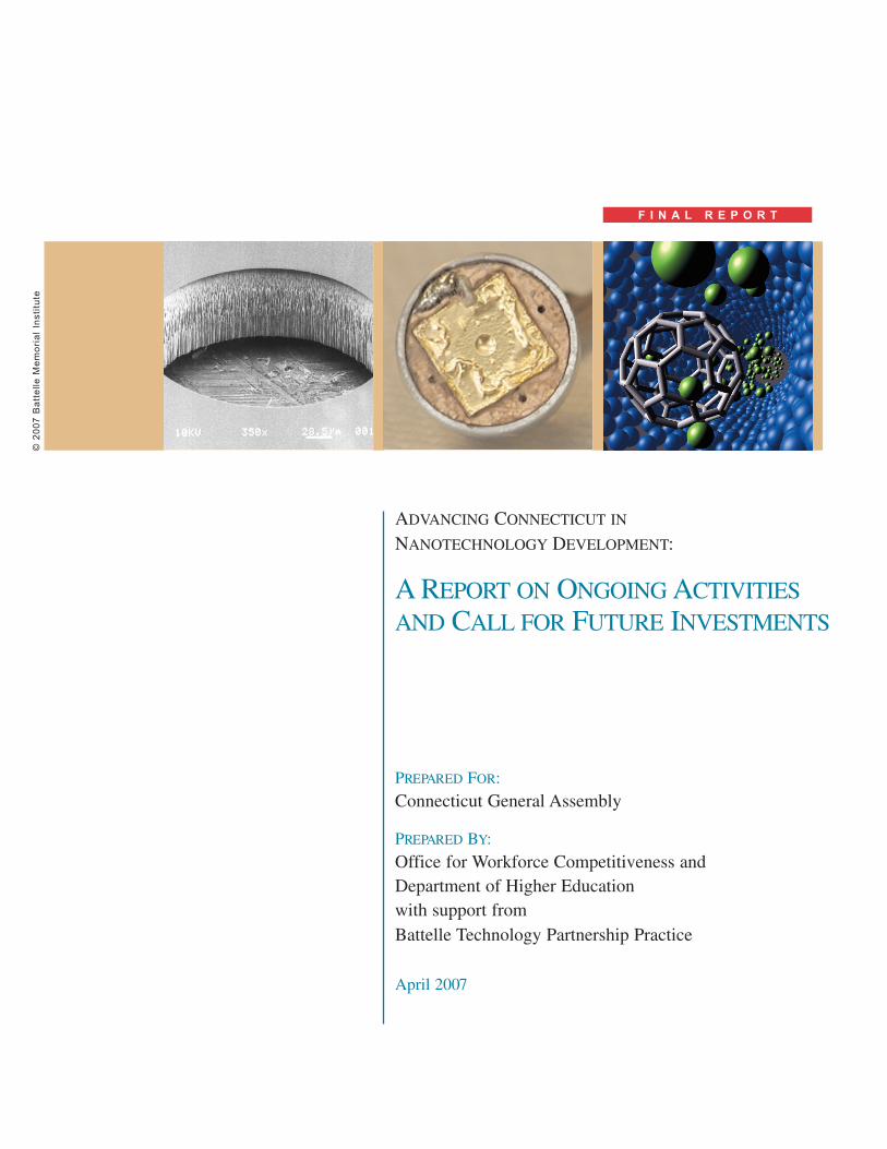
ADVANCING CONNECTICUT IN
NANOTECHNOLOGY DEVELOPMENT:
A REPORT ON ONGOING ACTIVITIESAND CALL FOR FUTURE INVESTMENTS
PREPARED FOR:
Connecticut General Assembly
PREPARED BY:
Office for Workforce Competitiveness and Department of Higher Educationwith support fromBattelle Technology Partnership Practice
April 2007
F I N A L R E P O R TNot for distribution or quotation.
CONTENTS
Introduction............................................................................................................................... 1
Update on SBIR-related Nanotechnology Product Innovation Initiative ................................. 3
Update on Post-Secondary Nanotechnology Education Program Development...................... 5
Update Nanotechnology University-Industry Collaboration Initiative .................................... 7
Update on Design of Connecticut Center for Nanoscale Sciences........................................... 9
Appendix A: Current and Future Nanotechnology Curriculum Development by Institution,
Instructor and Topics .............................................................................................................. 13
Appendix B: Listing of Existing Microscopy and Microanalysis Facilities in Connecticut .. 17
Appendix C: Listing of Proposed New and Upgraded Microscopy and Microanalysis
Capabilities for Physical and Life Sciences Applications ...................................................... 24
Battelle Memorial Institute (Battelle) does not endorse or recommend particular companies, products, services, or technologies nor does it endorse or recommend financial investments and/or the purchase or sale of securities. Battelle makes no warranty or guarantee, express or implied, including without limitation, warranties of fitness for a particular purpose or merchantability, for any report, service, data or other information provided herein.
Copyright 2007 Battelle Memorial Institute. Use, duplication, or distribution of this document or any part thereof is prohibited without the written permission of Battelle Memorial Institute. Unauthorized use may violate the copyright laws and result in civil and/or criminal penalties.
Update Overview: Key Progress to Date and Continuing Program Efforts and Investment Requirements
Over the past four years, Connecticut has been diligently at work in setting out a path for advancing nanotechnology development in the state. The efforts began with a detailed assessment of the value of emerging nanosciences to Connecticut and the state’s competitive position in nanotechnology. Based on those findings, a focused strategy was developed in concert with an Advisory Council drawn from industry, academia, government and economic development organizations.
Now Connecticut is piloting programs and activities to advance nanotechnology development in the state. These actions have been guided by specific legislation. Last year, pursuant to Public Act 05-198, Connecticut developed an action plan to advance nanotechnology development in 2006 in consultation with the Advisory Council for Nanotechnology. This action plan was well-received and enacted into legislation through Public Act No. 06-530, An Act Concerning The Advancement of Nanotechnology Development In Connecticut, along with an appropriation for FY 2006–2007 of $500,000.
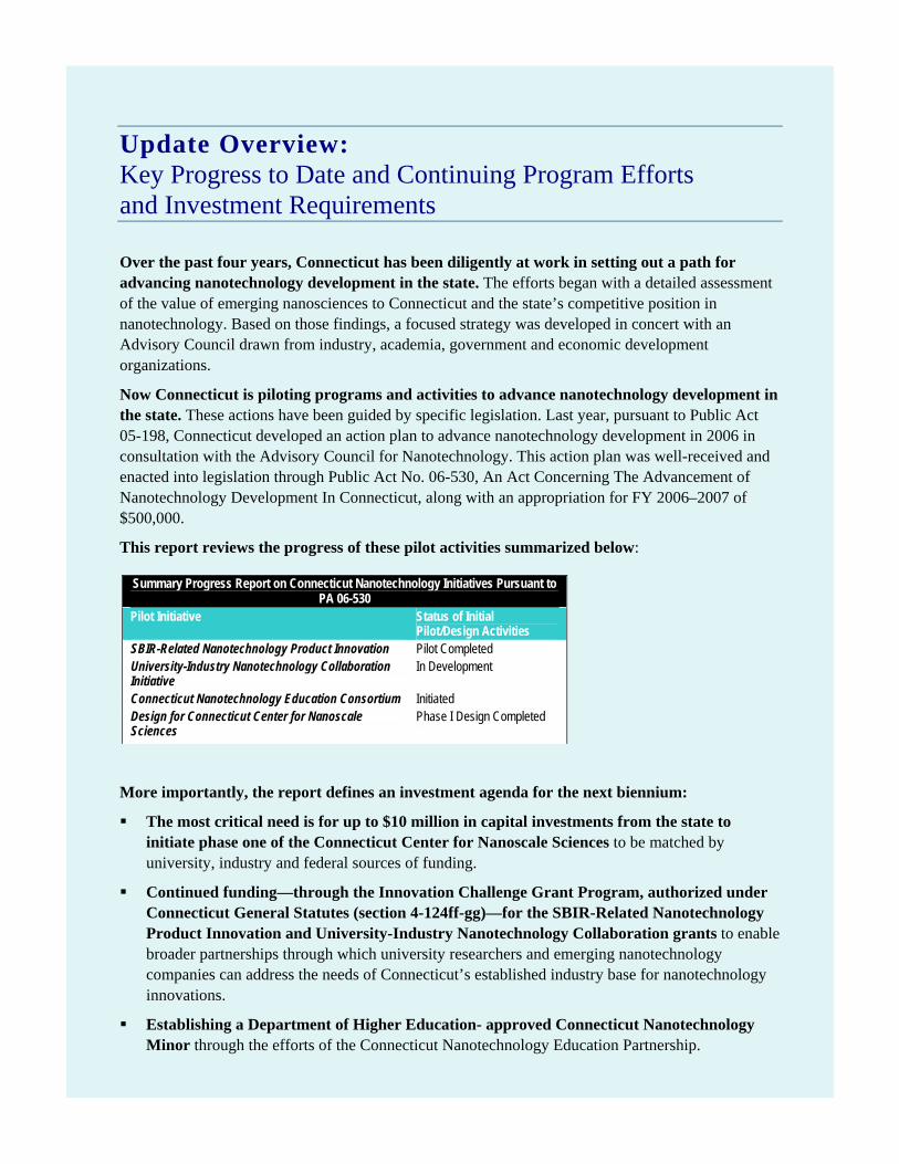
This report reviews the progress of these pilot activities summarized below:
More importantly, the report defines an investment agenda for the next biennium:
The most critical need is for up to $10 million in capital investments from the state to initiate phase one of the Connecticut Center for Nanoscale Sciences to be matched by university, industry and federal sources of funding.
Continued funding—through the Innovation Challenge Grant Program, authorized under Connecticut General Statutes (section 4-124ff-gg)—for the SBIR-Related Nanotechnology Product Innovation and University-Industry Nanotechnology Collaboration grants to enable broader partnerships through which university researchers and emerging nanotechnology companies can address the needs of Connecticut’s established industry base for nanotechnology innovations.
Establishing a Department of Higher Education- approved Connecticut Nanotechnology Minor through the efforts of the Connecticut Nanotechnology Education Partnership.
Summary Progress Report on Connecticut Nanotechnology Initiatives Pursuant to PA 06-530
Pilot Initiative Status of Initial Pilot/Design Activities
SBIR-Related Nanotechnology Product Innovation Pilot Completed University-Industry Nanotechnology Collaboration Initiative
In Development
Connecticut Nanotechnology Education Consortium Initiated Design for Connecticut Center for Nanoscale Sciences
Phase I Design Completed
– 1 –
Introduction
Over the past four years, Connecticut has been diligently at work in setting out a path for advancing nanotechnology development in the state. The efforts began with a detailed assessment of the value of emerging nanosciences to Connecticut and the state’s competitive position in nanotechnology. Based on these findings, a focused strategy was developed in concert with an Advisory Council drawn from industry, academia, government and economic development organizations. At the present time, Connecticut is piloting programs and activities to advance nanotechnology development in the state.
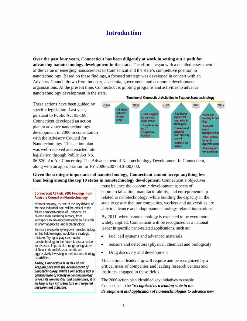
Timeline of Connecticut Activities to Support Nanotechnology
These actions have been guided by specific legislation. Last year, pursuant to Public Act 05-198, Connecticut developed an action plan to advance nanotechnology development in 2006 in consultation with the Advisory Council for Nanotechnology. This action plan was well-received and enacted into legislation through Public Act No. 06-530, An Act Concerning The Advancement of Nanotechnology Development In Connecticut, along with an appropriation for FY 2006–2007 of $500,000.
Given the strategic importance of nanotechnology, Connecticut cannot accept anything less than being among the top 10 states in nanotechnology development. Connecticut’s objectives
must balance the economic development aspects of commercialization, manufacturability, and entrepreneurship related to nanotechnology, while building the capacity in the state to ensure that our companies, workers and universities are able to advance and adopt nanotechnology-related innovations.
By 2011, when nanotechnology is expected to be even more widely applied, Connecticut will be recognized as a national leader in specific nano-related applications, such as:
• Fuel cell systems and advanced materials
• Sensors and detectors (physical, chemical and biological)
• Drug discovery and development
This national leadership will require and be recognized by a critical mass of companies and leading research centers and institutes engaged in these fields.
The 2006 action plan identified key initiatives to enable Connecticut to be “recognized as a leading state in the development and application of nanotechnologies to advance new
Connecticut At Risk: 2006 Findings from Advisory Council on Nanotechnology
Nanotechnology, as one of the key drivers of the next industrial age, will be critical to the future competitiveness of Connecticut’s diverse manufacturing sectors, from aerospace to advanced materials to fuel cells to pharmaceuticals and biotechnology. To miss the opportunity to grow in nanotechnology as this field emerges would be a strategic mistake. Trying to play catch up in nanotechnology in the future is also a recipe for disaster. In particular, neighboring states of New York and Massachusetts are aggressively investing in their nanotechnology capabilities. Today, Connecticut is at risk of not keeping pace with the development of nanotechnology. While Connecticut has a growing base of activity in nanotechnology across its universities and companies, it is lacking in key infrastructure and targeted development activities.
2003 2004 2005 2006•CT NanoInitiative formed (CNI)
• State support for nanotech assessment• Battelle study on CT Competitive Position
• Legislative support for nano educ & action plan•Formation of statewide nano advisory council• Action Plan drafted
2007
•PA 06-530 enacting Action Plan• $500,000 annual appropriate line• Pilot initiative design & implementation • Planning for new Biennium
– 2 –
products by existing and newly formed companies anchored by a set of well-established nanotechnology research and education assets across its public and private colleges and universities.”
These initiatives represent a tailored approach to nanotechnology development as part of the state’s Innovation Challenge Grant initiative (see PA 05-198), which provides Connecticut with the comprehensive tools required to advance the integrated goals of talent generation, university-industry collaboration and commercialization of university-based research.
Four specific initiatives were set out to advance Connecticut’s nanotechnology development:
• Establishing an active nanotechnology product innovation focus by building on the Connecticut Small Business Innovation and Research (SBIR) Office
• Pursuing a Connecticut Nanotechnology University/Industry Collaboration Initiative
• Advancing Post-Secondary Education Program Development in nanotechnology
• Developing the Connecticut Center for Nanoscale Sciences and Development, a shared use nanotechnology instrumentation facility with related programs.
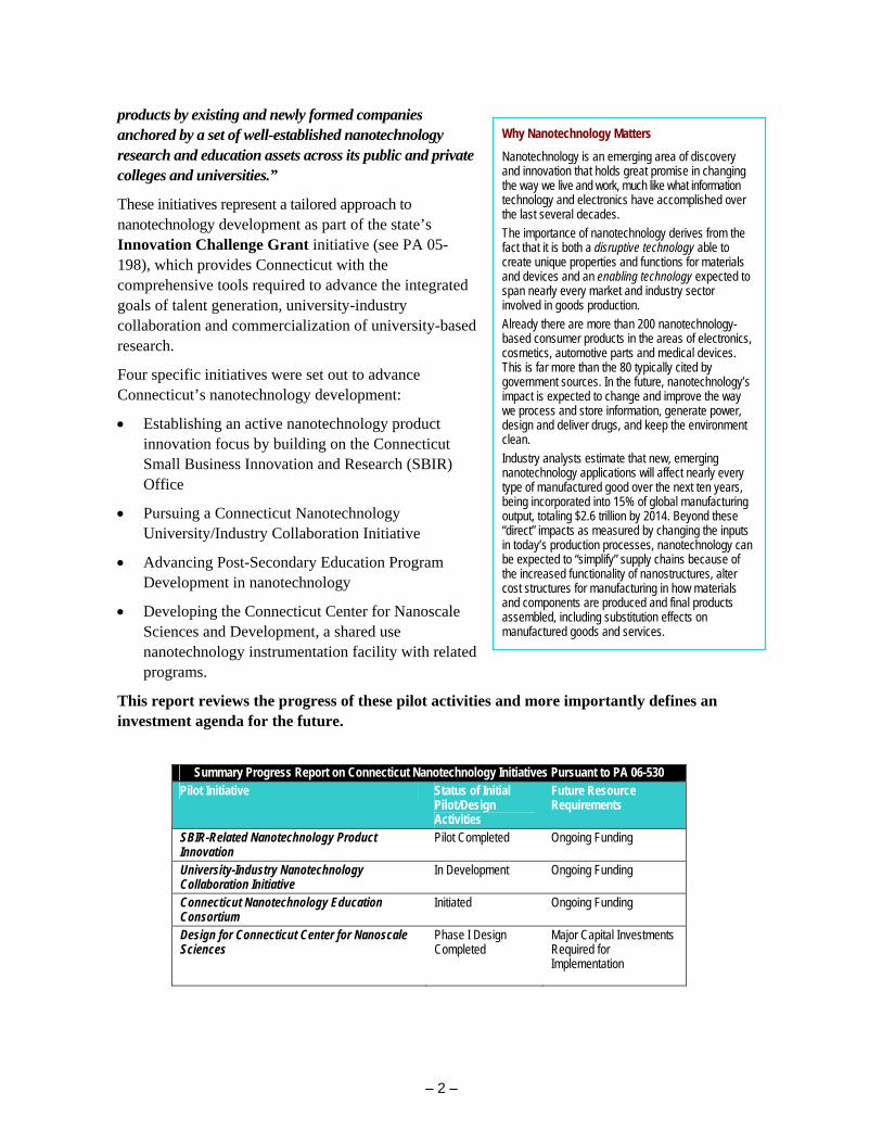
This report reviews the progress of these pilot activities and more importantly defines an investment agenda for the future.
Why Nanotechnology Matters
Nanotechnology is an emerging area of discovery and innovation that holds great promise in changing the way we live and work, much like what information technology and electronics have accomplished over the last several decades. The importance of nanotechnology derives from the fact that it is both a disruptive technology able to create unique properties and functions for materials and devices and an enabling technology expected to span nearly every market and industry sector involved in goods production. Already there are more than 200 nanotechnology-based consumer products in the areas of electronics, cosmetics, automotive parts and medical devices. This is far more than the 80 typically cited by government sources. In the future, nanotechnology’s impact is expected to change and improve the way we process and store information, generate power, design and deliver drugs, and keep the environment clean. Industry analysts estimate that new, emerging nanotechnology applications will affect nearly every type of manufactured good over the next ten years, being incorporated into 15% of global manufacturing output, totaling $2.6 trillion by 2014. Beyond these “direct” impacts as measured by changing the inputs in today’s production processes, nanotechnology can be expected to “simplify” supply chains because of the increased functionality of nanostructures, alter cost structures for manufacturing in how materials and components are produced and final products assembled, including substitution effects on manufactured goods and services.
Summary Progress Report on Connecticut Nanotechnology Initiatives Pursuant to PA 06-530 Pilot Initiative Status of Initial
Pilot/Design Activities
Future Resource Requirements
SBIR-Related Nanotechnology Product Innovation
Pilot Completed Ongoing Funding
University-Industry Nanotechnology Collaboration Initiative
In Development Ongoing Funding
Connecticut Nanotechnology Education Consortium
Initiated Ongoing Funding
Design for Connecticut Center for Nanoscale Sciences
Phase I Design Completed
Major Capital Investments Required for Implementation
– 3 –
Update on SBIR-related Nanotechnology Product Innovation Initiative
BACKGROUND The federal Small Business Innovation Research (SBIR) grant program sets aside a total of $2 billion for small and emerging companies to research and develop new technologies to solve federal agency problems. This research and development can then lead to the commercialization of new products and services.1 SBIR is a good fit with the needs of nanotechnology because it is targeted to small and emerging companies and to the critical need in nanotechnology of reduction to practice and prototype development. At the same time, the federal government is expected to be an early adopter and user of nanotechnology, given the need to find innovative solutions to needs ranging from defense systems to biomedical research to alternative energy applications. SBIR can be a key tool for federal agencies to identify, test and prototype specific nanotechnology applications.
Connecticut has established a state-supported SBIR program through the Office of Workforce Competitiveness (OWC) and operated by the Connecticut Center for Advanced Technology (CCAT). This effort has proven effective in informing companies about SBIR and raising the number of SBIR applications submitted by Connecticut companies, which had declining in recent years. In particular, the state-supported SBIR effort has developed active outreach and education programs for Connecticut companies to make them aware of SBIR opportunities and offers technical and business assistance for companies developing SBIR proposals. The Office has held a number of successful conferences and workshops and directly involved federal agency SBIR program managers in these activities.
A particularly successful strategy of Connecticut’s SBIR Office has been to link small CT companies with large defense contractors in Connecticut and beyond. The “Partner with a Prime [tm]” program matches small CT companies with large companies seeking innovative solutions that can be integrated into larger systems. Both parties stand to benefit, since the smaller technology companies can offer innovative solutions and capabilities to these large firms, who can then demonstrate to federal agencies the value of specific SBIR topics and proposals. This partnership tends to increase the chances of the small company being funded, as well as for the technology to eventually be commercialized.
PILOT INITIATIVE UNDERWAY Status: Pilot Completed Future Requirements: Ongoing funding support
The Connecticut SBIR office has developed an innovative partnering approach that enables large defense contractors in Connecticut to identify specific needs for the potential application of nanotechnology in support of Department of Defense initiatives. These identified need statements then serve as a solicitation for innovative new concept ideas from emerging Connecticut 1 The SBIR program solicitations are issued by eleven Federal agencies, including the Departments of Defense, Health and Human Services, Energy, Homeland Security, Agriculture, Commerce, Education, Transportation, NASA, NSF, and EPA. For more information about the SBIR program, visit http://www.sba.gov/sbir/indexsbir-sttr.html.
– 4 –
companies with nanotechnology capabilities. A review process involving the large defense contractor and independent experts, including academicians, then assesses the concept ideas proposed from a technical and business perspective. The goal is to provide a jump-start for an SBIR proposal that addresses a key Department of Defense need. Through an initial grant of $65,000—matched by the emerging technology company—initial data can be generated that can support a future SBIR proposal and build in a path to commercialization in partnership with Connecticut’s large defense contractors.
To pilot this approach, the Connecticut SBIR office at CCAT worked with Electric Boat to validate a critical need of the Navy requiring nanotechnology innovations. The overall theme is to apply nano-scale approaches to improving the performance and reducing the costs of fuel cells for unmanned vehicles.
Eight full proposals were received and then reviewed by a panel drawn from private industry, including Electric Boat, as well as research and technology organizations. The reviewers evaluated each of the proposals based on technical and business criteria, including technical feasibility, team capabilities, innovativeness, the potential to solve a market need, approach to commercialization and management team.
Three awards were made; projects were started in February 2007 and are expected to be completed within six months:
• MysticMD on the “The use of conductive carbon nanotube coatings for increased PEM fuel cell performance”
• Mott Corporation on the “Development of integrated all metal flow field electrode assemblies for fuel cells”
• GenCell Corporation on “Design, development and testing of bipolar plates with nano-scale coatings and catalysts for SOFC applications.”
More on Innovative Nanotech Companies Participating in Pilot SBIR Product Innovation Initiative
MysticMD is an early stage technology company in the advanced materials and coatings business. The company seeks to leverage and apply carbon nanotube technology based conductive coatings to a range of security, medical and industrial markets. The funded project is designed to develop an alternative carbon nanotube for Polymer Membrane (PEM) Fuel Cells. The objective is to both increase performance and reduce costs through the application of proprietary technology that uses lower concentrations of platinum than traditional carbon supported platinum systems and use the coating technology to create an integrated current collector. The project is intended to demonstrate the feasibility of this approach for both product performance and manufacturability. Mott Corporation is an established manufacturer founded in 1959, currently employing 165 people. The company produces large chemical filtration systems and specialty porous devices, as well as filters for semiconductor quality gases. This project is designed to develop an innovative approach which integrates nano-structured catalysts with electrodes in fuel cells, allowing these electrodes to be cleaned for reuse, thereby reducing the overall operating and life cycle costs of the fuel cell. GenCell Corporation, started in 1997, has developed a fuel cell bipolar plate and stack architecture that is “designed for manufacture” and can be applied cross-platform to many different fuel cell types and applications. This project is designed to demonstrate the application of a nanocatalyst to Gencell’s internal reforming chamber, with a focus on portable fuel cells for military applications. An initial set of fuels will be tested during this phase. The eventual goal is to establish a compact and economical Solid Oxide Fuel Cell (SOFC) product line suitable for unmanned vehicles.
– 5 –
Update on Post-Secondary Nanotechnology Education Program Development
BACKGROUND The emerging field of nanoscience is widely recognized as at the frontier for emerging research in the biological, engineering, and physical sciences. The field is a far-reaching revolution in the understanding and control of increasingly complex phenomena and systems at the nanoscale.
Nanotechnology is by its nature a multi-disciplinary field, drawing on the disciplines of physics, chemistry, biology, materials science and engineering. Yet, as the field is emerging, it is also becoming more specialized in the types of specific tools and techniques that it requires. This poses a question on how best to integrate nanotechnology into educational programs.
The question is how to incorporate nanotechnology—more properly, nanoscience—into college and university curriculums. One challenge is its highly multidisciplinary nature. Another challenge is the rapid pace of change occurring in the field, requiring that any curriculum be based on strong fundamentals of scientific knowledge that can enable students to change and grow along with the field.
Education and training in nanotechnology needs to be stimulated in Connecticut. Nanotechnology must be integrated more extensively into associates, bachelor’s, and master’s degrees, and not simply left to Ph.D. programs. A number of Connecticut higher education institutions are already engaged in developing a nanotechnology curriculum. The goal should be to share approaches, fill needed gaps in curriculum development, and address access to instructional laboratories across higher education.
FORMATION OF A CONNECTICUT NANOTECHNOLOGY EDUCATION CONSORTIUM Under the direction of the Department of Higher Education, a Connecticut Nanotechnology Education Consortium has been convened. This consortium includes nine higher education institutions, with participation by the Dean of Science and Engineering or their representative and directors of interdisciplinary centers and institutes or their representatives . The mission of the Consortium is to construct the intellectual foundation of nanoscience and nanotechnology education at the post-secondary level in Connecticut and to help ensure appropriate workforce development in nanotechnology and in supporting scientific and technical fields. Dr. Lou Manzione, Dean of the School of Engineering at the University of Hartford, is serving as the first chair of the Consortium.
The long-term objective of the Consortium is to develop a “Connecticut Nanotechnology Minor” that all post-secondary institutions in Connecticut can implement. This Connecticut Nanotechnology Minor would offer a standard four or five course sequence across all participating Connecticut colleges and universities. It would be available to all students, no matter what their major. It would be reviewed for content annually and would be revised as the field
Participating Institutions in the Connecticut Nanotechnology Education Consortium Central Connecticut State
University The College of
Technology/Community College System
Fairfield University Southern Connecticut State
University University of Bridgeport University of Connecticut University of Hartford University of New Haven Yale University
– 6 –
evolved. Because it would be state developed and endorsed,, the Connecticut Nanotechnology Minor would not create issues or concerns with national or field-specific accreditors.
One of the first steps taken by the Connecticut Nanotechnology Education Consortium has been to inventory existing and future courses in nanotechnology by institution (see Appendix A).
PILOT INITIATIVE UNDERWAY Status: Pilot Initiated Future Requirements: Ongoing funding support
To initiate efforts towards establishing a Connecticut Nanotechnology Minor, the first two courses are under development:
An overview course, at the introductory level, that provides a foundation in nanoscience and nanotechnology.
A topics course crafted around the economic and industrial/business needs of the state.
Working groups drawn from faculty across all participating higher education institutions in the Consortium are being formed to prepare these two courses. The process for developing these standard curricula is being facilitated by the Department of Higher Education.
In addition, the Department of Higher Education has completed inventories of nanotechnology curriculum and identified faculty in Connecticut involved in nanotechnology curriculum and courses.
– 7 –
Update Nanotechnology University-Industry Collaboration Initiative
BACKGROUND A key finding from the Assessment of Connecticut’s Nanotechnology Position study was that “the vast majority of Connecticut companies with the opportunity to integrate nanotechnologies are acting as spectators rather than participants. Because nanotechnology is such a rapidly evolving field, much of the action in advancing nanotechnology is taking place in the basic research laboratories found in universities. The key question is whether Connecticut companies will be able to gain the skill sets and knowledge to advance and commercialize nanotechnology and whether that activity will take place in Connecticut.”
The goal of this initiative is to increase the awareness by industry of nanotechnology tools and innovations to speed their adoption in Connecticut. A Nanotechnology University-Industry Collaboration Initiative for Connecticut can help to build closer ties between Connecticut’s university capacity and expertise in nanotechnology and the state’s broad base of technology firms. Such collaboration will also serve as a means for developing and retaining critical nanotechnology talent in Connecticut by engaging graduate students and post-docs. Ultimately, the Nanotechnology University-Industry Collaboration Initiative should contribute to creating a superior environment for advancing the “business” of nanotechnology in Connecticut.
PILOT INITIATIVE IN DEVELOPMENT Status: Pilot In Development Future Requirements: Ongoing funding support
One way to better enable Connecticut companies to make this leap into nanotechnology development is to broaden industry collaborations with colleges and universities in Connecticut through joint projects typically involving graduate students and post-doctoral fellows with faculty guidance. The University-Industry Collaboration Initiative is being designed and initial pilot activities are planned to start in the spring of 2007.
The objective is to build and support teams conducting “pre-competitive” research in which industry driven needs or university opportunities of interest to industry are further developed in advance of actual product development or commercialization. Thus, the focus will be on projects addressing problems facing industry, where using nanotechnology tools can provide insights or demonstrate the potential to address market opportunities, or on discoveries from university laboratories showing commercial promise where industry is willing to work with the faculty member to reach the next step in development of the idea. This pre-competitive research will typically be in advance of actual commercialization or product development.
The intent would be to encourage a collaborative effort involving companies and university groups to address specific problem statements or pursue a significant opportunity based on university research discoveries. A team would include, at a minimum, a small company setting the agenda in response to a market need or opportunity vetted by a larger company, with work conducted by a graduate student/post doctoral fellow with guidance by a faculty member.
An emphasis will be placed on “enabling activities” to foster collaboration and strategic alliance skills development. The planned initiative will focus on facilitating dialogues between
– 8 –
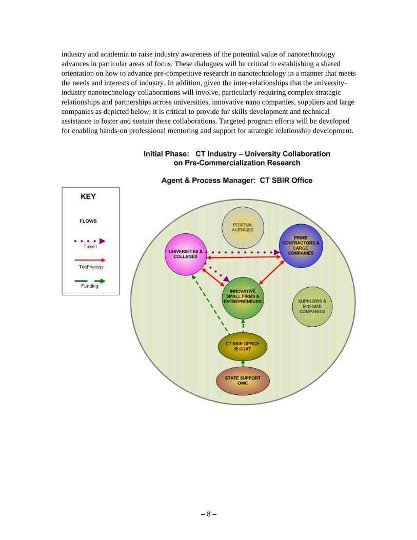
industry and academia to raise industry awareness of the potential value of nanotechnology advances in particular areas of focus. These dialogues will be critical to establishing a shared orientation on how to advance pre-competitive research in nanotechnology in a manner that meets the needs and interests of industry. In addition, given the inter-relationships that the university-industry nanotechnology collaborations will involve, particularly requiring complex strategic relationships and partnerships across universities, innovative nano companies, suppliers and large companies as depicted below, it is critical to provide for skills development and technical assistance to foster and sustain these collaborations. Targeted program efforts will be developed for enabling hands-on professional mentoring and support for strategic relationship development.
– 9 –
Update on Design of Connecticut Center for Nanoscale Sciences
BACKGROUND In nanotechnology, the critical starting point for developing, measuring, and testing applications is the use of advanced high-resolution, high-sensitivity instrumentation, whether related to academic research or industrial product development. The promise of nanotechnology was significantly advanced in the 1980s and 1990s with the advent of new tools to see and manipulate individual atoms and molecules and now we are able to translate that scientific research into commercial activities.
Connecticut already has in place numerous shared use facilities that cater to the needs of academic and industrial users (see listing in Appendix B). A recent field review conducted by a national nanotechnology expert on behalf of the state of Connecticut found that existing instrumentation facilities in Connecticut are at a competent level, although somewhat specialized by scientific discipline. Connecticut lacks the state-of-the-art instrumentation for more comprehensive nanoscale characterization (higher structural resolution and detection sensitivity) and faster throughput for applications in the physical and life sciences. So, while Connecticut’s existing nanoscale instrumentation may be adequate to “get the job done,” it falls well short of offering “go to” signature facilities that will provide a competitive advantage for researchers, education programs and companies seeking to advance new product innovations.
The specific gaps in nanoscale instrumentation found in Connecticut, include:
• Advanced tools for “complete” characterization (physical/chemical, organic/inorganic,; bulk/surface)
• High-resolution imaging and high-sensitivity analysis capabilities
• Full line of sample preparation equipment
• Structural simulation and molecular modeling tools
• Clean rooms and fabrication lines for prototyping
• Tools for studying the structure and chemistry of surfaces and interfaces
Given the high cost and technical support required to operate sophisticated nanotechnology tools, it is best to organize these nanotechnology tools in shared-use laboratories. This allows for a broad access to academic and industry researchers, while promoting specific applications development in focused fields of activity.
The value of a shared-use nanotechnology instrumentation facility goes well beyond enhancing a university’s competitiveness for federal grants; it also can enable nanotechnology discoveries to be more quickly advanced for proof-of-concept and future testing. A nanotechnology instrumentation facility can also offer an important “hands-on” component for nanotechnology-related education and training programs.
– 10 –
PHASE ONE INVESTMENT RECOMMENDATION: ADVANCING MICROSCOPY AND MICROANALYSIS TO INITIATE THE CONNECTICUT CENTER FOR NANOSCALE SCIENCES AND DEVELOPMENT
Status: Phase I Design Completed Future Requirements: Major Capital Investment Required to Implement
The first step in advancing the Connecticut Center for Nanoscale Sciences and Development is to establish a shared-use facility for advanced microscopy and microanalysis to address physical sciences and life sciences related applications. The need for easily accessible, state-of-the-art microscopy and microanalysis capabilities has been expressed by academic researchers, as well as scientists working in small and large companies within Connecticut dealing with a broad range of applications. Advanced electron microscopy (transmission and scanning modes), as well as optical microscopy and scanning probe microscopy capabilities, are needed (see Appendix C for representative listing of equipment needs).
Microscopy and microanalysis facilities have different requirements for physical and life sciences in terms of the specific equipment, instrumental techniques, sample preparation, and personnel required:
• Applications in the physical sciences range from device fabrication and systems integration of sensors and actuators (MEMS), failure analysis in semiconductor devices and jet engines, to characterization of materials for the space shuttle and stealth aircraft, to building better cars and bridges.
• Applications in the life sciences range from supporting diagnoses in human pathology to the study of autoimmune diseases such as AIDS and arthritis, and reach across medical , pharmaceutical, agricultural, dental, and related fields.
These differences call for facilities dedicated specifically to the physical sciences and the life sciences. While these dedicated facilities can be co-located or distributed among different locations, given the extensive physical sciences instrumentation already found at the University of Connecticut (UCONN), Storrs and extensive life sciences facilities at Yale and the UConn Health Center, a distributed approach may make more sense.
It is recommended that:
• Electron microscope platforms be selected that can offer universal imaging and analysis solutions for life sciences, materials sciences, nanotechnology, and the semiconductor and opto-electronics industries. For example, leading scanning/transmission electron microscope platforms should be selected that can enable ultra-high-resolution imaging, analysis and characterization for a range of applications at sub-Ångström levels. By offering fully- integrated, automated and high throughput capacity, costs per sample would be reduced without compromise in performance. A wide variety of advanced microscopy systems exist to select from include from FEI, JEOL, Hitachi and Zeiss.
• Existing microscopes be upgraded where possible with digital imaging and analysis capabilities as well as detectors for chemical analysis. In addition, sample holders that enable environmental studies of samples to be performed in situ under simulated operating conditions should be purchased for labs focused on relevant physical and life science
– 11 –
applications such as fuel cells, sensors and cell pathology. New ancillary equipment must be added for sample preparation in order to reach the full imaging and analysis potential of the new and upgraded microscopes. Back-up power supplies are needed to maintain continuous operation of instruments in case of unexpected power outages or shutdowns. This will ensure that academic researchers and product developers have access to the “best” tools and techniques to get the job done correctly, rapidly, easily and cost-effectively.
• Expert staff be hired in the physical and life sciences that understand problem-solving and the importance of detail in instrument operation and maintenance. This will make certain that users shall have access to technical support, training and consultation, as well as help to perform a range of services.
• A CT microscopy and microanalysis network be created that links the various shared-user centers and stand alone facilities through an outreach and liaison function established through the Connecticut Center for Nanoscale Sciences.
Funding Requirements
For this first phase in establishing the Connecticut Center for Nanoscale Sciences and Development, several key cost parameters can be identified:
• Acquisition of Advanced Microscopy Instrumentation: A one-time purchase of two top-tier electron microscopes, one customized for physical sciences and one for life sciences.
Estimated Funding Requirements: $8 to $9 million in one-time instrumentation • Ancillary Equipment: Associated with this advanced microscopy instrumentation are costs
for sample preparation and data analysis tools.
Estimated Funding Requirements: $2 to $3 million in one time instrumentation costs • Facilities to house instrumentation: For both the life sciences and physical sciences
advanced microscopy instrumentation system, a facility of 3,000 sq ft with enhanced air handling, low vibration, higher floor heights, back-up generation and high security is required. The estimated cost for these facilities with utilities is expected to run $35 to $50 per sq ft or $210,000 to $300,000 per year.
Estimated Funding Requirements: Up to $300,000 annually
• User Support and Ongoing Maintenance: Two teams of expert staff to operate the facilities, offer technical support to users and conduct ongoing maintenance are needed at an estimated cost of $1 million per team annually. Each team is expected to have one Ph.D. level scientist skilled in either the physical or life sciences who understands the technical and commercial aspects of solving nanotechnology problems. In addition, there should be at least two support staff skilled in sample preparation and instrument operation and maintenance. Service contracts with microscope, detector and other equipment manufacturers will be required to ensure that instruments run safely, without interruption, and to the highest performance standards.
Estimated Funding Requirements: Up to $2 million annually
– 12 –
• Outreach and liaison function: This would include a lead program manager and an associate, with resources for marketing materials, in-state travel and database systems.
Estimated Funding Requirements: Up to $350,000 annually.
Thus, the total cost over five year associated with Phase I development of the Connecticut Center for Nanoscale Sciences are approximately $23 to $25 million, comprised of:
• One time instrumentation purchase costs of $10-12 million for advanced microscopy instrumentation systems and ancillary equipment.
• Annual operating costs of $2.65 million, or $13.25 million over five years for expert user technical support, outreach and liaison functions and facility costs.
– 13 –
Appendix A: Current and Future Nanotechnology Curriculum Development
by Institution, Instructor and Topics
A. CURRENT INSTRUCTION REGARDING NANOTECHNOLOGY:
Central Connecticut State University (CCSU), Hoopengardner Potential of nanotechnology, prospective use of
nanotechnology in nucleic acid regulation, clinical relationships, delivery mechanisms of nanotechnology
CCSU, Crundwell Nanowires, physical nature of conduction via band
theory (Desc. Inorganic Chemistry)
CCSU, Westcott Doping and band theory for semi and superconducting materials (Desc. Inorganic Chemistry)
CCSU, Watson Nanoscience and nanotechnology, nanodevices for
drug delivery and implantation materials used for joint and tissue repair
Southern Connecticut State University (SCSU), Broadbridge PHY 231 (Physics for Scientists and Engineers),
1 lecture introductory concepts; PHY309L (Modern Physics), 3 lectures: nanoscience and tools of nanotechnology; IDS 571& SCE 575 (Science Laboratory Practice and Integrated Science Experience): pre-service and in-service science teachers, graduate level, 80% of course, teaches training and knowledge necessary to carry out research projects, nanoscience and materials science, tools, and ethical issues; PHY 499 & 471, Independent Studies, practical and theoretical knowledge, techniques
Univ of Bridgeport, Xiong Micro-electromechanical System (whole semester
course) Micro-fabrication (nanotechnology 20% of course)
University of Connecticut (UCONN) Budnick, Stwalley PHYS 325, “Selected topics in Nanoscale Science”
– 14 –
UCONN New Courses ECE 250, 251 Nanotechnology-I and Nanotechnology - II
UCONN, Huey MMAT 298 Nanomaterials University of Hartford Nanotechnology briefly mentioned in numerous
courses University of New Haven Special Topics Nanoscale Sciences (PH-450/ME Sinha 450): overview of Nanomaterials, no lab Introduction to Nanotechnology (EE-670) grad
level, focused on Nano-devices and sensors, no lab Honors course on Fuel cells and Global Hydrogen
Economy Yale University, Reed Introduction to Nanoscience: survey course for
freshmen: Realistic nanosystems, method for fabrication, physical properties and applications of nanostructures, MEMS, biological applications and system architecture
B. INTEREST IN DEVELOPMENT OF COURSES AND/OR PROGRAMS: CCSU, Crundwell Introductory General Science Course
CCSU, Westcott Organometallics Course: basic prin. leading up to organometallic polymers (molecular wires)
CCSU, Watson Seminar in Nanoscience: bring in professionals
giving a scope to the field and contacts for employment
Cell Biology of Cellular Implants Protein Interactions with implanted materials (lab) SCSU, Broadbridge Special Topics to introduce nanoscience and
nanotechnology: Sophomore level for a variety of backgrounds; Upper-level course with emphasis on interdisciplinary applications
Univ. of Bridgeport, Xiong Introduction to Nanotechnology, including origins
and nature, impact to society, current research issues, scaling effect, physics for nanotechnology, carbon and Si based nano materials, nanofabrication, tools, nanoscale electronics, NEMS, and nanofluidics and bio applications
– 15 –
UCONN Papadimitrakopoulus, Interdisciplinary Graduate Program in Nanobionics. Birge and others
UCONN, Jain Undergraduate plan of study in electrical and
computer engineering “Nanotechnology for Devices and Systems”
UCONN, Huey A two course undergraduate minor in
Nanotechnology MMAT Thin Films and Coatings course in
development UCONN, Burkhard MCB Nanotechnology course in development UCONN, Stuart Biosensors course under development University of Hartford Would like to develop an Introductory course in Moslehpour nanotechnology and its application to
electrical/computer engineering. The course would include nanofabrication techniques including STM, AFM, molecular self -assembly, nanoimprint and soft lithography, DNA-based assembly, and MEMS-based multi-probe systems. Other topics included, such as carbon nanotubes and quantum dots.
University of Hartford Math courses that would use curriculum content to Grant simulate visual interactive and computational
properties of specific nanotechnology University of Hartford Considering courses in Micro and Nano Fluidics, Milanovic Micro and Nano Flow Modeling and Fundamentals,
Nanoscale modeling, Two-Phase Micro Fluidics, Integrated Micro Fluidic Systems
University of Hartford Would develop Environmental Engineering Pines graduate course w/ nanomaterials treatment
applications as sensors and risk University of Hartford Eppes Technical Concentration: Mechanical Engineering,
Mechanical Engineering Technology, and Electrical Engineering Technology. Nano Photonic Processing Technology (course) Optical and Material Interaction Properties (course)
– 16 –
University of Hartford Develop new course in air pollution and prevention Filburn methods University of Hartford Develop an Advanced Topics Course in Manzione Nanotechnology Applications (graduate level open
to seniors)—would include major advances in nanotechnology
Also interested in a non-majors variation of nanotechnology applications
University of New Haven 2 semester lab nanotechnology: needs Sinha instrumentation
3 week Module on Nanotechnology for Spiral Eng. Program Would like to develop a course for forensics students on nanomaterials/nanotechnology
C. MODIFICATION OF CURRENT COURSES:
CCSU, Hoopengardner General concepts and prospective uses of nanotechnology (Intro course)
Potential use of nanotechnology for quantization of physiologic states
Nanotechnology and RNA interference, microRNAs
CCSU, Crundwell Adv. Inorganic chem. Lab: fabrication and
identification of nanomaterials University of Hartford Water Quality Engineering and Adv. Water Quality Pines Eng.—increased coverage of application of
nanomaterials in water with case studies
– 17 –
Appendix B: Listing of Existing Microscopy and Microanalysis
Facilities in Connecticut
UNIVERSITY OF CONNECTICUT
The Institute of Materials Science (IMS)
Microscopy Laboratory http://www.ims.uconn.edu/~micro/ The Institute of Materials Science (IMS) at the University of Connecticut (UConn) is an interdisciplinary center with the threefold mission of fostering education, research and outreach in all areas of the materials sciences. The Microscopy Laboratory is one of several major user facilities within the IMS, and houses the main research microscopes used by students, staff and faculty within the Institute, and by colleagues, collaborators and affiliates from elsewhere.
The laboratory currently has two TEMs including a high-resolution instrument, and three SEMs together with a wide variety of optical microscopes, scanning probe microscopes, sample preparation and other ancillary equipment. Electron Microscopy JEOL 2010 FasTEM transmission electron microscope that provides information regarding the morphology, crystallography and elemental composition for advanced materials. This is a 200kV instrument with a thermionic electron source and four high-resolution CCD cameras that allow images to be acquired digitally. The 2010 FasTEM has an ultra-high resolution pole-piece, giving a lattice resolution of 0.14nm. It is equipped with a Gatan Imaging Filter (GIF 2000), which enables electron energy loss spectroscopy (EELS) and energy filtered imaging to be performed that can dramatically improve image contrast and resolution in the TEM, and allow highly sensitive elemental maps to be obtained. Energy dispersive X-ray spectroscopy (EDS) can be undertaken using an EDAX Phoenix system. Quantitative and qualitative chemical analysis of materials can be undertaken using either EDS or EELS.
Philips EM420 TEM is equipped with a 120 kV thermionic electron source and provides a lattice resolution of 0.3nm. Accessories include: a STEM system, back-scattered and secondary electron detectors, and a Noran Quest EDS unit. This microscope is ideal for routine TEM investigations, EDS elemental mapping, and for training new TEM users.
TEM sample preparation equipment includes two ion-mills, an electro-polisher, an ultrasonic disc cutter, a precision saw, a dimpling machine, a core drill and a disc punch. Software for the simulation and analysis of lattice images, diffraction patterns and defects is available on both PC and Mac platforms. The laboratory is equipped with both an Edwards E306A Coating System and a Polaron E5100 SEM Coating Unit.
AMRay 1000A SEM is furnished with the Microspec WDX-2A wavelength dispersive X-ray system and the Noran Quantum thin window, energy dispersive X-ray system.
Philips ESEM 2020 is an environmental SEM and is equipped with an EDAX CDU/SUTW thin window, EDS system. A Peltier Stage is also available for in-situ experiments.
JEOL 6335F Field Emission SEM is a cold cathode field emission scanning electron microscope. It has a resolution of 1.5nm at 15kV and 5.0nm at 1kV. The sample stage is fully automated, with
– 18 –
computer control. This instrument is equipped with a state-of the art Thermo-Electron EDS system for chemical microanalysis including mapping and spectrum imaging.
An additional soft materials TEM capability and sample preparation instrumentation is operated in the Molecular Cell Biology multi-instrument Electron Microscopy Laboratory.
Optical Microscopy Polarized-light microscopes are available for crystallographic and morphological studies and phase identification of transparent materials. Heating and cooling stages and time-lapse cinemicrography can be combined to study phase changes, liquid-crystal transformations, equilibrium composition diagrams, and solidification processes in a temperature range from -60°C to 1,200°C. Principal instruments include:
Leitz Quantitative Interference Microscope is available for surface roughness and/or thin film thickness determination.
Linkam Programmable Thermal Analysis System is a digitally controlled system for controlled heating or cooling (-196ºC to 600°C) while simultaneously viewing the sample.
Nikon Labophot Polarizing & Olympus Vanox Universal Research Microscopes are available for transmitted light techniquesSupplemental compensators are available for polarized light measurements; phase contrast, dispersion staining, refractive index determination, and micrometry.
Scanning Probe Microscopy Scanning Probe Microscopy (SPM) allows surface characterization from the micrometer down to the nanometer scale. Although typically used to map topography, SPM can be configured for mapping a wide variety of materials properties.
Asylum Research MFP-3d is a cutting edge atomic force microscope (AFM) with sub-nanometer and nanoNewton resolution. The device is configured to measure local topography, mechanical compliance, piezoactuation, and electric and magnetic fields. Top and bottom view optics allow precise tip-sample positioning.
Asylum Research MFP-3d-IO is mounted directly on a Nikon inverted optical microscope for simultaneous AFM and bright field optical imaging. A temperature and fluid controller is available, making this instrument ideal for biological or electrochemical investigations.
Omicron UHV AFM/STM is a high resolution ultra high vacuum unit capable of atomic scale resolution with atomic force or scanning tunneling microscopy (STM) modes, measured independently or simultaneously. Scanning tunneling spectroscopy additionally allows local electronic states to be probed.
An additional AFM is available in chemistry.
UConn Health Center (UCHC)
Farmington, CT
http://www.uchc.edu/ Central Electron Microscope Facility (CEMF) http://resadm.uchc.edu/hcrac/electronmicroscopy.html The Central Electron Microscope Facility (CEMF) is a Health Center supported research facility providing electron microscopy research service for faculty, students and extramural users. The CEMF has two transmission electron microscopes and a high-resolution field emission scanning
– 19 –
electron microscope. Sample preparation equipment includes ultramicrotomes, vacuum evaporator, sputter coater and ion beam coater.
Services available include: complete processing, examination and photography of TEM (thin-sections) and SEM specimens; negative staining of particulate samples; cryosectioning; immunofluorescence and immunogold labeling; freeze-fracture; rotary shadow.
Center for Cell Analysis and Modelling (CCAM) Microscopy Facility http://www.ccam.uchc.edu/microscopy_facility/microscopy_facility.html The CCAM Microscopy Facility is open to the UCHC research community as well as other academic and industrial institutes.
There are five confocal microscopes, a wide-field fluorescence microscope, sample preparation equipment, as well as computational and other support functions.
YALE UNIVERSITY
Nanotechnology Laboratory
The Nanotechnology Laboratory has equipment for high resolution e-beam lithography, SEM characterization facilities, AFM and STM in both ambient and UHV environments, and an exceptionally wide range of device analysis capabilities. The laboratory specializes in the fabrication and investigation of nanostructured, quantum, and novel molecular scale devices.
The laboratory is also equipped for research in MEMS, with ODE etching and thin film membrane expertise, and has full facilities of two clean rooms for conventional MOS processes. We have facilities for chemical preparation (fume hoods, NMR, etc.) and extensive expertise in their characterization for research in molecular and biological systems, focusing on the integration with microelectronics.
Interdepartmental Program in Vascular Biology and Transplantation (VBT) Facilities
Research grade optical microscopes including a fluorescence microscope and a confocal fluorescence microscope; a cryomicrotome; a fluorescence activated cell sorter, scintillation counters, a laser densitometer, a phosphor imager, multiple centrifuges, freezers, plus temperature control rooms (warm and cold).
Materials Characterization Facility
Atomic force microscopes, scanning tunneling microscopes, and scanning electron microscopes for analyzing semiconductor surfaces; an energy and wavelength dispersive x-ray microprobe for chemical analysis.
Environmental Engineering Equipment
Multimode Scanning Probe Microscope with an assortment of tips and accessories for wet and dry scanning. The atomic force microscope is equipped with a high magnification top view optical microscope for accurate tip positioning and monitoring.
Optical microscope with software for image analysis, CCD camera, analog to digital converter for rapid dynamic image acquisition. An assortment of bright and dark field objectives for viewing very small (submicrometer) colloidal particles, biological samples, and surfaces.
– 20 –
Mechanical Testing Laboratory
Scanning electron microscope for materials characterization and micromechanical testing of small-scale structures of various materials. It provides a high resolution digital image acquisition system, an EDS unit for chemical analysis of materials, a OIM unit for microtexture characterization of individual crystals, custom-built loading stages and heating stages, and an infrared CCD monitoring camera. Digital image correlation software and related hardware have also been recently developed to process digital images acquired from the scanning electron microscope, optical microscope, and the CCD and video cameras for whole-field deformation mapping.
Center for Research on Interface Structures and Phenomena (CRISP) A National Science Foundation Materials Research Science and Engineering Center (MRSEC)
http://www.crisp.yale.edu/ CRISP has access to a diverse and powerful assembly of microscopy facilities, with laboratories at all three CRISP locations, Yale and Southern Connecticut State Universities (New Haven, CT) and Brookhaven National Laboratory (Upton, NY).
Facilities at Yale include Scanning Electron Microscopy (SEM), Transmission Electron Microscopy (TEM), Scanning Tunneling Microscopy (STM) and Atomic Force Microscopy (AFM), in addition to the ongoing development within CRISP of atomic resolution non-contact AFM and magnetic AFM.
The NanoCharacterization Facility located at SCSU provides nanoscale microscopy and microanalysis of the elemental composition of materials. This facility is equipped for advanced materials research as well as for education and outreach and is staffed by highly skilled, professional electron microscopists. SCSU’s microscopy instrumentation includes AFM, SEM and TEM equipped with scanning transmission electron microscopy (STEM). X-ray energy dispersive spectroscopy (EDS) is available on both SEM and TEM. Advanced light microscopy (LM) is also available.
Brookhaven’s Center for Functional Nanomaterials (CFN) has advanced electron microscopy facilities (http://www.bnl.gov/cfn/facilities/microscopy/) and is home to the Center for Advanced Electron Microscopy (CAEM). CAEM (http://www.bnl.gov/TEM/) combines world-class instrumentation with a team of leading materials scientists). Capabilities include:
• TEM Analysis – including high resolution imaging, electron diffraction, energy dispersive x-ray analysis, and electron energy loss spectroscopy.
• SEM Analysis – including imaging, image analysis, and both quantitative and qualitative x-ray analysis.
• Scanning Auger – surface analysis, imaging, and depth profiling.
– 21 –
Yale School of Medicine Center for Cell and Molecular Imaging (CCMI) and X-ray Crystallography
CCMI is dedicated to provide state-of-the-art imaging facilities and technical support to all investigators at the medical school and interested investigators on the main campus. Biomedical research increasingly relies on imaging, not only of tissues but at the cellular and molecular level as well. Indeed, investigators from virtually every department and section use our facilities.
Imaging resources include:
• Confocal and two-photon microscopy
• Electron microscopy
• Cryo-electron microscopy
• Cellular systems design
CCMI: Confocal Microscopy http://cellserv.med.yale.edu/imaging/ccmi/confocal.html Confocal microscopy enables the visualization and imaging of fixed as well as living cells and tissues that contain fluorescent probes (antibodies, green fluorescent proteins, dyes, substrates). This technique allows sharply defined optical sections to be collected, from which three dimensional rendering and movies can be created.
The confocal facility is a shared resource that offers two laser scanning confocal microscopes and a combined confocal/two-photon microscope to Yale investigators. It provides access and training to both confocal and two photon microscopes, related equipment and image workstations.
CCMI: Electron Microscopy http://cellserv.med.yale.edu/imaging/ccmi/electron.html Mission is to provide electron microscopy services and techniques to investigators at Yale School of Medicine, offering a wide range of services from conventional EM to cryosectioning and immunogold labeling. Experienced staff can carry out all the steps of sample preparation and analysis for a set fee. Alternatively, facility is open to users who have had prior training in electron microscopy.
Equipment includes two transmission electron microscopes, ultramicrotomes, cryostat, evaporator, microwave processor, freeze-substitution unit, and dark room.
CCMI: Cryo-Electron Microscopy http://cellserv.med.yale.edu/imaging/ccmi/cryo_electron.html The electron cryomicroscopy facility (cryoEM) was jointly established by the Departments of Molecular Biophysics and Biochemistry and Cellular and Molecular Physiology to provide Yale faculty and staff with access to state-of-the-art imaging capabilities for the structure determination of macromolecular biological complexes. Because of the complex nature of molecular microscopy projects, this facility does not offer direct services. Instead, interested investigators usually meet with one of the directors to discuss feasibility of the project.
The core facility houses two cryo-capable transmission electron microscopes with room temperature holders and cold stages, pumping stations for film and cold holders, and other
– 22 –
accessory equipment for making carbon support films, glow discharge of grids, and a dark room for the development of electron micrographs.
CCMI: Cellular Systems Design Center http://cellserv.med.yale.edu/imaging/ccmi/cellular.html The Cellular Systems Design Center is an engineering group that assists the Yale community to fully utilize the latest imaging technologies. New technologies such as 2-photon imaging, total internal reflectance imaging, and others promise new avenues by which the function of cells and cellular systems can be studied.
CSDC projects range in complexity from designing basic custom components that fulfill a specific need for a particular experiment to creating exotic integrated systems that push the envelope of imaging technology. They design and fabricate custom components, add new detectors to microscopes, design enclosures, write acquisition software and more. They also integrate imaging systems with other instruments to make complete, coordinated experiments.
Yale School of Medicine Renal Pathology and Electron Microscopy http://www.yalepath.org/DEPT/specialty/emlab.htm The Yale Electron Microscopy and Renal Pathology Laboratory is a nationally recognized center for diagnostic electron microscopy and renal pathology. It provides the most effective methodologies available for ultrastructural and immunological diagnosis. These include transmission electron microscopy, negative staining, immunocytochemistry, and standard and confocal immunofluorescence techniques. There is special emphasis on the diagnosis of glomerular, tubulointerstitial, and vascular kidney diseases. Electron microscopy is also of value in the diagnosis of ciliary abnormalities, metabolic disorders, microbial identification, and tumor diagnosis. As one of the few such comprehensive electron microscopy services with digital imaging capability in the nation, it is well positioned to serve a wide geographic area with rapid turnaround combined with expert consultative services.
SOUTHERN CONNECTICUT STATE UNIVERSITY
NanoCharacterization Facility http://home.southernct.edu/~broadbridgc1/Facilities.htm The NanoCharacterization Facility located at SCSU provides nanoscale microscopy and microanalysis of the elemental composition of materials. This facility is equipped for advanced materials research as well as for education and outreach and is staffed by highly skilled, professional electron microscopists. SCSU’s microscopy instrumentation includes AFM, SEM and TEM equipped with scanning transmission electron microscopy (STEM). X-ray energy dispersive spectroscopy (EDS) is available on both SEM and TEM. Advanced light microscopy (LM) is also available.
A wide range of sample preparation instrumentation enables vacuum evaporative and sputter coating for SEM and low-angle/low-voltage ion milling for TEM. Sophisticated polishing tools, an ultramicrotome, and ancillary instrumentation are also available. These tools precisely and reproducibly permit routine preparation of materials for EM and AFM observation. The facility also provides an array of data and image processing software.
– 23 –
TRINITY COLLEGE
Electron Microscopy Facility http://www.trincoll.edu/~alehman/ Scanning tunneling and atomic force microscopes, two transmission electron microscopes (one for life sciences and one for materials sciences), two scanning electron microscopes, analytical support instrumentation (EDS), fully-featured sample preparation facilities, and both print and digital data acquisition capabilities.
WESLEYAN UNIVERSITY
Molecular Biology and Biochemistry Advanced Instrumentation Center http://www.wesleyan.edu/mbb/grad/grad_facilities.html Cell biological imaging equipment includes a Zeiss Axioplan fluorescence microscope equipped with CFP/YFP/GFP/Rhodamine filter sets and a Zeiss MRM Digital camera, a Zeiss confocal microscope and digital camera, and transmission and scanning electron microscopes.
– 24 –
Appendix C: Listing of Proposed New and Upgraded Microscopy
and Microanalysis Capabilities for Physical and Life Sciences Applications
ELECTRON MICROSCOPY TEM lattice image (300 KV), EELS; 3D reconstruction; cryo stage; soft material; Omega filter; custom specimen holders
SEM low voltage, field emission; orientation mapping; environmental
OPTICAL MICROSCOPY Nomarski, confocal; coupled to fluorescence analytical
SCANNING PROBE MICROSCOPY Standard (contact, tapping, shear, …)
Conductive/EFM
Structured tip PMs
Magnetic force
In liquid
Time resolved (pulsed, …)
Sample Preparation
Dual-Beam Focused Ion Beam Apparatus
Wet lab/fab (mostly bio)


![1[1].00060 A - Flexmate K500 Service Manual New Version 2 ... · warranties, express or implied, or statutory, including but not limited to the implied warranties of merchantability](https://img.pdfslide.us/doc/110x75/60292420e6bf5616904c5710/1100060-a-flexmate-k500-service-manual-new-version-2-warranties-express.jpg)