Embed Size (px)
Citation preview

AUTONOMOUS LOCAL CONTROL IN DISTRIBUTED DC POWER SYSTEMS
Robert S. Balog, Ph.D. Department of Electrical and Computer Engineering
University of Illinois at Urbana-Champaign, 2006 Philip T. Krein, Adviser
This dissertation investigates local control techniques that are applied to individual components in
a dc power system. These local controls operate autonomously using locally obtained information,
sensed at their respective components. Yet, they contribute to overall system stability without requiring
a central controller or peer-to-peer communication network. In the event of a disturbance in the dc
system, whether ephemeral or cataclysmic, autonomous local controls enable the system to self-heal in
the sense that unaffected components still operate. Load priority ensures that if energy is limited, the
most important loads have preferential access. Limited system knowledge, such as the overall health of
the system or change in mission objective, can be used to fine tune the controller performance.
However, the controllers still operate autonomously if access to this information is lost. These controls
are ideal for high-reliability, advanced energy systems since they can perform system-level coordination
and are fault-tolerant.
Applications considered are supply-side and demand-side management. On the supply side, droop
control is examined as a form of autonomous local control that adds damping to stabilize the power
system. On the demand side, control strategies are shown for both single bus and multibus systems. In
a single bus system, dynamic load interruption is shown to be useful to prevent voltage collapse, when
demand exceeds supply, and to be capable of automatic load restoration upon system stabilization. In
a multibus system, autonomous local controls can ensure reliable system operation by reconfiguring
how the load is supplied to ensure seamless power transfer during fault conditions or partial loss of
generation.

© 2006 by Robert S. Balog. All rights reserved.

AUTONOMOUS LOCAL CONTROL IN DISTRIBUTED DC POWER SYSTEMS
BY
ROBERT S. BALOG
B.S., Rutgers University, 1996 M.S., University of Illinois at Urbana-Champaign, 2002
DISSERTATION
Submitted in partial fulfillment of the requirements for the degree of Doctor of Philosophy in Electrical Engineering
in the Graduate College of the University of Illinois at Urbana-Champaign, 2006
Urbana, Illinois


iii
ABSTRACT
This dissertation investigates local control techniques that are applied to individual
components in a dc power system. These local controls operate autonomously using locally
obtained information, sensed at their respective components. Yet, they contribute to overall
system stability without requiring a central controller or peer-to-peer communication network.
In the event of a disturbance in the dc system, whether ephemeral or cataclysmic, autonomous
local controls enable the system to self-heal in the sense that unaffected components still
operate. Load priority ensures that if energy is limited, the most important loads have
preferential access. Limited system knowledge, such as the overall health of the system or
change in mission objective, can be used to fine tune the controller performance. However,
the controllers still operate autonomously if access to this information is lost. These controls
are ideal for high-reliability, advanced energy systems since they can perform system-level
coordination and are fault-tolerant.
Applications considered are supply-side and demand-side management. On the supply
side, droop control is examined as a form of autonomous local control that adds damping to
stabilize the power system. On the demand side, control strategies are shown for both single
bus and multibus systems. In a single bus system, dynamic load interruption is shown to be
useful to prevent voltage collapse, when demand exceeds supply, and to be capable of
automatic load restoration upon system stabilization. In a multibus system, autonomous local
controls can ensure reliable system operation by reconfiguring how the load is supplied to
ensure seamless power transfer during fault conditions or partial loss of generation.

iv
To my Wife

v
ACKNOWLEDGMENTS
First and foremost, I owe a debt of gratitude to my adviser, Dr. Philip T. Krein. I value the
opportunity to have worked with him and appreciated his support as I undertook a number of
nondissertation related projects which broadened my background. He always gave me plenty
of latitude to explore new ideas and new areas. Dr. Krein’s mentorship has taught me to
examine the fundamental elements of a problem and to dig deeply into the archives to link my
contribution with the past work of others. I am also thankful for the support he provided so
that I may attend numerous professional conferences to present my work, interact with the
larger community, and grow professionally.
I would like to thank the members of my doctoral committee for their guidance and
suggestions. Their enduring influence was to help me understand the importance of relating
and explaining my work to the broader community. I would like to thank Dr. Peter Sauer for
his many heartfelt words of encouragement and support and Dr. Patrick Chapman for always
being available for technical consultation and honest career advice. I appreciated their personal
interest and counsel, particularly this past year while my adviser was away on sabbatical. I also
thank my other committee members: Dr. Thomas Overbye for providing many useful insights
into challenges in the ac utility system and Dr. Christoforos Hadjicostis for providing an
outside perspective and motivating me to think about the larger field of fault-tolerant controls.
In addition to my committee, I would like to thank Dr. M. Anantha Pai for his
encouragement and Dr. George Gross for his personal interest. I would also like to
acknowledge and thank Dr. Dieter Vandenbussche for his help in formulating the bilevel
mathematical programming abstraction in Chapter 5 and Dr. Daniel Liberzon for many
discussions on switched systems which helped solidify the mathematical notation in the
discussion on state-dependent switching in Chapter 6. Although I self-identify as an
experimentalist, my conversations with Dr. Vandenbussche and Dr. Liberzon helped me to
gain an appreciation for mathematical abstraction.

vi
Success in any endeavor is always contingent upon the confluence of great people. To
compile a comprehensive list of everyone who has helped me achieve my pursuits is an
intractable problem. So to everyone I send a heartfelt thank you. I would be remiss, however, if
I neglected to mention a few extraordinary people. First, I emphatically thank Joyce Mast for
her countless hours of technical writing support. Although I may not have always appeared
receptive, her suggestions have helped shape my discordant, incoherent paragraphs into
melodic exposition – or as much as could be expected from an engineer. In addition, she has a
uniquely positive outlook on life and takes great personal interest in the students she works
with. I would also like to thank Karen Driscoll and her predecessors in the administrative
office for their support and personal interest. It was always cathartic to commiserate with
Karen over the seemingly nebulous bureaucratic web of the University. I would also like to
thank Karen Chitwood for “breaking me in” when I first arrived on campus.
Many thanks go out to my colleagues who either helped me directly or were just good
company. In particular I would like to thank Jonathan Kimball for his many useful
suggestions, help with coordination of the laboratory, and mostly just acting as a sanity check.
Joseph Mossoba is not only my respected colleague but also a great friend – despite the mild
hazing I put him through. Joe and I have complimentary skill sets that enabled us to work
extremely well together. I look forward to having the opportunity to work with both Jonathan
and Joe in the future. Xin Geng was a terrific officemate and helped me drudge through the
mathematics. I would also like to thank those who initially welcomed me into the group and
have long since graduated: Dimitrios Chaniotis, Pedro Correia, Santiago Grijalva, Mike
Kokovec, Daniel Logue, Trong Nguyen, and Cesar Pascual.
I enjoyed the opportunity to work with many talented and ambitious undergraduate lab
assistants including Andrew Niemerg, Brian Raczkowski (now a UIUC graduate student),
Nathan Brown, and Leonor Linares. In particular, Scott Donahue and David Schmitz were
tremendously helpful with the experimental portions of this dissertation.
The Department of Electrical and Computer Engineering is greatly enhanced by the
quality service of the machine shop and electronics services shop. Both of these organizations
have my sincere gratitude and respect. In the machine shop, I wish to thank Scott McDonald

vii
and Bob Feller who almost always refrained from laughter whenever I proudly displayed my
mechanical drawings, and never ran out of constructive advice. I would like to also thank the
rest of the group – Jim, Greg, Scott, and Craig – for their technical expertise, without which I
would not have had quality experimental hardware. Despite their rough exteriors, these guys
really do care. In the electronics shop, Dan Mast has been a tremendous resource. His Rolodex
of contacts is invaluable when equipment needs to be purchased or when it doesn’t work as
advertised and customer service places you in the voice-mail shuffle. He always has plenty of
advice, is eager to share it, and seems to truly love working with students. As for the rest of his
group, they are the reason why the laboratory facilities at Illinois are second to none. I thank
Jim, Frank, Gary, Earl, and Norm for all their help. In today’s reality of budget cuts, the
machine shop and electronics shop provide vital services that enhance the quality and
reputation of the UIUC program and distinguishes it from other institutions. I encourage the
department to continue unwavering support.
On a personal note, although I came to Illinois to pursue my graduate studies, life is more
than just work. I am fortunate to have met some truly wonderful people and to have made
many great memories. One of the first people I met was Greg Uhrhan when I rang the
doorbell at the Kappa Delta Rho fraternity house. Although I was not a member of the UIUC
chapter and was more than a few years older than the undergraduates, Greg and the others
welcomed me and were an instant source of friends in an otherwise strange land. It was
through KDR that I met Chris Hickersberger and Gwendolyn Chen. The Graduate Student
Advisory Council provided an opportunity to socialize with graduate students in different
departments and disciplines. It was there that I met Mike Persia, Bryan Dunne, and Kimberly
Buchar. I am lucky to have met such wonderful friends and I hope that we remain so even as
life takes us in different directions.
I thank my family for all of their support and encouragement: my mother who has always
been a source of strength, support, and encouragement; my father who for a short 14 years
was my best friend, mentor, and role model; my uncle who was always there as a sounding
board with wise words of advice; and my sister for encouraging my scholastic pursuits. The
English language is crude and unrefined with the term “in-law.” Teşekurederim anne ve baba

viii
who welcomed me into their family with open arms, as if I was their own son, and Ayşegül
who loves me as if I was her own brother even though I stole her abla.
Although listed last here, she is first in my heart and the person to whom I dedicate this
dissertation – my wife, Ülkü. Mere words cannot explain the happiness, love, and sense of
completion that I feel having her in my life. I could not imagine completing this work without
her support. This chapter in our lives has come to an end, but I will forever fondly recall that
“I met my wife while we were both in grad school.”
This work was supported in part by the National Science Foundation and the Office of
Naval Research under EPNES Grant No. ECS-0224829 and by the Grainger Center for
Electric Machinery and Electromagnetics (CEME) at the University of Illinois at Urbana-
Champaign.

ix
TABLE OF CONTENTS
LIST OF FIGURES......................................................................................................... xii LIST OF TABLES..........................................................................................................xvii ACRONYMS, ABBREVIATIONS, AND TERMINOLOGY................................... xviii CHAPTER 1 INTRODUCTION...................................................................................... 1
1.1 Examples of High-Reliability DC Systems ...........................................................................2 1.1.1 Telecommunications power systems.......................................................................3 1.1.2 Naval combat survivability test-bed.........................................................................3 1.1.3 Underwater scientific observatories.........................................................................5 1.1.4 Spacecraft......................................................................................................................6 1.1.5 Distributed generation and microgrids ...................................................................7
1.2 Why Direct Current Systems? .................................................................................................8 1.3 Controls to Improve Reliability ........................................................................................... 13
1.3.1 Droop control........................................................................................................... 14 1.3.2 Dynamic load interruption ..................................................................................... 14 1.3.3 Bus selection.............................................................................................................. 15 1.3.4 Load priority.............................................................................................................. 15
1.4 Common Control Structures................................................................................................ 15 1.4.1 Centralized control................................................................................................... 16 1.4.2 Agent systems ........................................................................................................... 17 1.4.3 Multiagent systems................................................................................................... 18
1.5 Demonstration System for a DC Architecture with Autonomous Local Controls......................................................................................................................... 19
1.6 Organization ............................................................................................................................ 20 CHAPTER 2 MODELING .............................................................................................23
2.1 Controller Model .................................................................................................................... 23 2.2 Reduced-Order Modeling ..................................................................................................... 25
2.2.1 Small-signal analysis ................................................................................................. 27 2.2.2 Example comparison............................................................................................... 30
2.3 Scaled-Power Modeling......................................................................................................... 30 2.3.1 Analysis....................................................................................................................... 32 2.3.2 Example: Scaled output filter, constant parasitic resistances ........................... 33 2.3.3 Example: Scaled output filter and parasitic resistances..................................... 36
2.4 Conclusion ............................................................................................................................... 38 CHAPTER 3 STABILITY ISSUES IN DISTRIBUTED DC SYSTEMS.....................39
3.1 Power System Stability........................................................................................................... 40 3.1.1 Maximum power transfer ....................................................................................... 40 3.1.2 Dynamic impedance of loads................................................................................. 43 3.1.3 Voltage stability......................................................................................................... 44
3.2 Dynamic Coupling in a DC System .................................................................................... 45 3.3 Input Filters ............................................................................................................................. 46 3.4 Middlebrook Stability Criterion ........................................................................................... 47

x
3.5 Middlebrook Extra Element Theorem............................................................................... 49 3.6 Damped Input-Filter Design................................................................................................ 51 3.7 Extension of Middlebrook Criterion to Arbitrary System Interface ............................ 52 3.8 Beyond the Middlebrook Criterion..................................................................................... 53 3.9 Conclusions.............................................................................................................................. 56
CHAPTER 4 LOCAL CONTROL..................................................................................57 4.1 Load-Control Strategies for System Stability..................................................................... 58 4.2 Transient Time Scales ............................................................................................................ 59
4.2.1 Short-term transients ............................................................................................... 60 4.2.2 Long-term transients................................................................................................ 61
4.3 Load Prioritization and Scheduling..................................................................................... 62 4.4 Nature of the Disturbance.................................................................................................... 63 4.5 Integrated Local-Control Strategy ....................................................................................... 63 4.6 Example Applications............................................................................................................ 66
4.6.1 Inrush current protection ....................................................................................... 66 4.6.2 Priority-dictated load shed in a radial dc bus ...................................................... 68
4.7 Conclusions.............................................................................................................................. 69 CHAPTER 5 SINGLE-BUS SYSTEMS..........................................................................70
5.1 Supply-Side: Droop Control................................................................................................. 72 5.1.1 Steady-state stabilization ......................................................................................... 73 5.1.2 Dynamic stabilization .............................................................................................. 75
5.2 Load-Side: Dynamic Load Interruption............................................................................. 79 5.2.1 The P-V curve........................................................................................................... 79 5.2.2 Simulation example.................................................................................................. 81
5.3 Voltage-Based Load Interruption........................................................................................ 83 5.3.1 Power flow analysis.................................................................................................. 85 5.3.2 Converter efficiency................................................................................................. 86 5.3.3 Contingency analysis................................................................................................ 88 5.3.4 Search algorithm....................................................................................................... 89 5.3.5 Experimental results ................................................................................................ 91
5.4 dv/dt-Based Dynamic Load Interruption ......................................................................... 93 5.5 Combined Under Voltage and dv/dt Load Shed............................................................. 96 5.6 Signal Conditioning ................................................................................................................ 97 5.7 Bilevel Programming.............................................................................................................. 99 5.8 Impedance-Based Online Measurements ........................................................................ 101 5.9 Conclusions............................................................................................................................ 102
CHAPTER 6 BUS SELECTION IN MULTIBUS SYSTEMS ................................... 105 6.1 Bus Selection: Auctioneering Diodes................................................................................ 106
6.1.1 Experimental results .............................................................................................. 109 6.2 Bus Selection: Active Control ............................................................................................ 111 6.3 Simulation Results ................................................................................................................ 113 6.4 Stable Bus Selection with State Dependent Switching .................................................. 120
6.4.1 System transient response..................................................................................... 121 6.4.2 Bus impedance loading effect .............................................................................. 124
6.5 Conclusions............................................................................................................................ 126 CHAPTER 7 CONCLUSIONS..................................................................................... 127

xi
7.1 Future Work .......................................................................................................................... 128 REFERENCES .............................................................................................................. 130 APPENDIX A EXPERIMENTAL HARDWARE DETAILS..................................... 143
A.1 Point-of-Load Buck Converter .......................................................................................... 143 A.1.1 Buck converter PCB silkscreen ........................................................................... 145 A.1.2 Buck converter schematics ................................................................................... 146 A.1.3 Buck converter filter inductor design ................................................................. 153 A.1.4 Buck converter ripple ............................................................................................ 153 A.1.5 Buck converter small-signal analysis................................................................... 157
A.2 Point-of-Load Supervisor Controller................................................................................ 162 A.2.1 PIC controller functional layout.......................................................................... 163 A.2.2 PIC controller PCB silkscreen ............................................................................. 165 A.2.3 PIC controller schematics..................................................................................... 166
A.3 Supervisor Control Firmware............................................................................................. 171 A.3.1 Main program.......................................................................................................... 171 A.3.2 LCD driver subroutines ........................................................................................ 190
APPENDIX B MATLAB POWER FLOW SEARCH ALGORITHM........................ 193 CURRICULUM VITA ................................................................................................... 198
xii
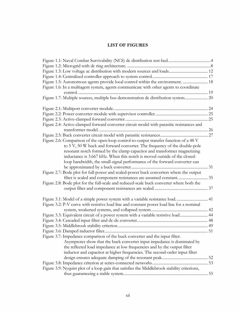
LIST OF FIGURES
Figure 1.1: Naval Combat Survivability (NCS) dc distribution test-bed...........................................4 Figure 1.2: Microgrid with dc ring architecture. ....................................................................................8 Figure 1.3: Low voltage ac distribution with modern sources and loads....................................... 12 Figure 1.4: Centralized controller approach to system control........................................................ 17 Figure 1.5: Autonomous agents provide local control within the environment. ......................... 18 Figure 1.6: In a multiagent system, agents communicate with other agents to coordinate
control. .................................................................................................................................. 19 Figure 1.7: Multiple sources, multiple bus demonstration dc distribution system....................... 20 Figure 2.1: Multiport converter module............................................................................................... 24 Figure 2.2: Power converter module with supervisor controller..................................................... 25 Figure 2.3: Active-clamped forward converter. .................................................................................. 25 Figure 2.4: Active-clamped forward converter circuit model with parasitic resistances and
transformer model. ............................................................................................................. 26 Figure 2.5: Buck converter circuit model with parasitic resistances................................................ 27 Figure 2.6: Comparison of the open-loop control-to-output transfer function of a 48 V
to 5 V, 50 W buck and forward converter. The frequency of the double-pole resonant notch formed by the clamp capacitor and transformer magnetizing inductance is 3.667 kHz. When this notch is moved outside of the closed-loop bandwidth, the small-signal performance of the forward converter can be approximated by a buck converter............................................................................. 31
Figure 2.7: Bode plot for full-power and scaled-power buck converters where the output filter is scaled and component resistances are assumed constant. ............................. 35
Figure 2.8: Bode plot for the full-scale and reduced-scale buck converter where both the output filter and component resistances are scaled. ..................................................... 37
Figure 3.1: Model of a simple power system with a variable resistance load. ............................... 41 Figure 3.2: P-V curve with resistive load line and constant power load line for a nominal
system, weakened systems, and collapsed system......................................................... 42 Figure 3.3: Equivalent circuit of a power system with a variable resistive load............................ 44 Figure 3.4: Cascaded input filter and dc-dc converter....................................................................... 48 Figure 3.5: Middlebrook stability criterion........................................................................................... 49 Figure 3.6: Damped inductor filter........................................................................................................ 51 Figure 3.7: Impedance comparison of the buck converter and the input filter.
Asymptotes show that the buck converter input impedance is dominated by the reflected load impedance at low frequencies and by the output filter inductor and capacitor at higher frequencies. The second-order input filter design ensures adequate damping of the resonant peak.............................................. 52
Figure 3.8: Impedance criterion at series-connected networks........................................................ 53 Figure 3.9: Nyquist plot of a loop gain that satisfies the Middlebrook stability criterions,
thus guaranteeing a stable system..................................................................................... 55

xiii
Figure 3.10: Nyquist plot of loop-gain with superimposed GMPM and ESAC forbidden regions. .................................................................................................................................. 55
Figure 4.1: Control structure to autonomous local controllers. Sensed information
remains in situ. ..................................................................................................................... 57 Figure 4.2: Power buffer for a DC system........................................................................................... 60 Figure 4.3: Sustaining time capability [124]. ........................................................................................ 61 Figure 4.4: Control strategy for an autonomous, load-side load controller................................... 64 Figure 4.5: Flowchart for inrush current controlled startup............................................................. 66 Figure 4.6: Simulation of startup inrush conditions for buffered and unbuffered
operation............................................................................................................................... 67 Figure 4.7: Radial dc system. .................................................................................................................. 68 Figure 5.1: Single bus radial test system with three loads. ................................................................ 70 Figure 5.2: Droop-controlled voltage source. ..................................................................................... 73 Figure 5.3: Current sharing using droop-control................................................................................ 74 Figure 5.4: Initial system transient response for a lightly damped system..................................... 76 Figure 5.5: Bus current at each POL converter. At 5 s the load increases at bus1. The
previously stable system becomes unstable with growing oscillations. At 5.5 s, the droop resistance at the source converter is adjusted to restabilize the system. ............................................................................................................................ 77
Figure 5.6: Bus voltage at each POL converter. At 5 s the load increases at bus 1. The previously stable system becomes unstable with growing oscillations. At 5.5 s, the droop resistance at the source converter is adjusted to restabilize the system. ............................................................................................................................ 78
Figure 5.7: P-V curve showing operating points as the system impedance increases and loads are interrupted. .......................................................................................................... 80
Figure 5.8: Ideal bus voltage and load power as system impedance increases and loads are interrupted to prevent voltage collapse. ................................................................... 80
Figure 5.9: Voltage collapse as load increases. .................................................................................... 82 Figure 5.10: POL converter 2 is shed at 2.0 s, allowing higher priority loads 1 and 3 to
remain active. As additional load is added to the system at 3.0 s, converter 1 is shed, preserving system stability and allowing the highest priority load, 3, to remain active. .................................................................................................................. 83
Figure 5.11: Control introduces chattering into the system. ............................................................ 84 Figure 5.12: Model of a radial dc power system with a single source and three point-of-
load converters. ................................................................................................................... 85 Figure 5.13: Outer loop of power flow algorithm incorporating converter efficiency. .............. 86 Figure 5.14: Curve fit for experimental efficiency data. .................................................................... 88 Figure 5.15: Results of exhaustive contingency analysis on the radial test system with a
single source and three point-of-load converters. The load on each converter can be either off, base load, or overload. Solid bars indicate contingencies where a bus voltage in the system is below the UVP for that converter.................. 90
Figure 5.16: System voltages drop in response to an increase in loading at POL3. Since the new terminal voltage for POL3 is below the UVP, it will trip off-line to self-protect............................................................................................................................ 92

xiv
Figure 5.17: The lowest priority load (POL2) is shed following the increase at POL3, thus allowing the higher priority loads 1 and 3 to remain on. .................................... 93
Figure 5.18: The lowest priority load (POL2) is shed to preserve voltage stability as the system is progressively loaded. ......................................................................................... 94
Figure 5.19: Controller does not respond to a slowly decreasing bus voltage. ............................. 95 Figure 5.20: Rapid decrease in bus voltage triggers load shed. ........................................................ 96 Figure 5.21: Response to progressive voltage collapse where undervoltage load shed
turns off the lowest priority load followed by dv/dt based load shed for the medium priority load. ......................................................................................................... 97
Figure 5.22: Undervoltage load interruption of POL2 shortly after 0.62 s followed by dv/dt triggered load interruption of POL1 in response to increase in rate of decline of system voltage. .................................................................................................. 98
Figure 5.23: Bus voltage at each point-of load converter. Without load interruption (dotted lines) the bus voltage collapses and POL3 falls out of regulation. With dynamic load interruption enabled (solid lines), because the load at POLC2 is shed, the bus voltages remain strong. ........................................................ 103
Figure 5.24: Impedance ratio at the interface between the point-of load converter and the system. Without load interruption (dotted lines) the impedance ratio for POLC3 drops below unity. With dynamic load interruption enabled (solid lines) the impedance ratio at each converter is prevented from remaining near unity. ........................................................................................................................... 104
Figure 6.1: Dual bus redundant system.............................................................................................. 105 Figure 6.2: Diode OR’ed dual buses supplying a resistive load. .................................................... 107 Figure 6.3: Forward bias characteristics of the MUR3040PT [174].............................................. 108 Figure 6.4: Diode OR’ed dual buses supplying a dc-dc point-of-load converter....................... 109 Figure 6.5: Current sharing in a diode OR'ed dual bus system with resistive load. ................... 110 Figure 6.6: Current sharing in a diode OR'ed dual bus system with closed-loop buck
converter load. ................................................................................................................... 111 Figure 6.7: Dual bus system with active-switched bus selection supplying a dc-dc point-
of-load converter............................................................................................................... 112 Figure 6.8: Dual bus system with bus converters and auctioneering diodes............................... 112 Figure 6.9: Dual bus system after change in source impedance using auctioneering
diodes. ................................................................................................................................. 113 Figure 6.10: Dual bus system after change in source impedance using ideal switch
selection. ............................................................................................................................. 115 Figure 6.11: The bus selector switches from the primary bus (bus1) to the alternate bus
(bus2) at 1.3 s following a change in system impedance at 1.0 s. This results in the highest voltage for the downstream load converter........................................ 116
Figure 6.12: The bus selector switches from the primary bus (bus1) to the alternate bus (bus2) at 1.3 s following a change in system impedance at 1.0 s. However, this does not result in the highest output voltage. Thus, at 1.6 s the controller switches back to the primary bus. .................................................................................. 117
Figure 6.13: Bus selection using bus controllers and auctioneering diodes. Bus controllers respond to changing bus voltage by adjusting the output voltage V1 and V2 so that diode action smoothly commutates current from one bus to the other..................................................................................................................................... 118
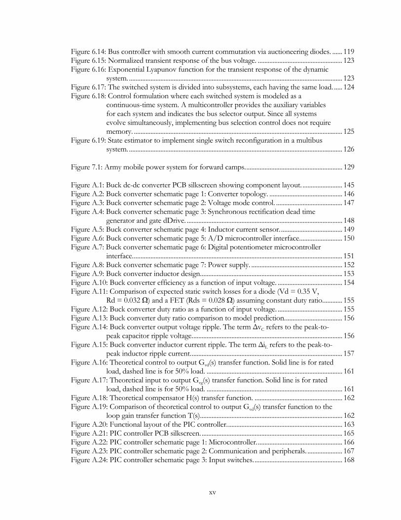
xv
Figure 6.14: Bus controller with smooth current commutation via auctioneering diodes. ...... 119 Figure 6.15: Normalized transient response of the bus voltage. ................................................... 123 Figure 6.16: Exponential Lyapunov function for the transient response of the dynamic
system.................................................................................................................................. 123 Figure 6.17: The switched system is divided into subsystems, each having the same load. ..... 124 Figure 6.18: Control formulation where each switched system is modeled as a
continuous-time system. A multicontroller provides the auxiliary variables for each system and indicates the bus selector output. Since all systems evolve simultaneously, implementing bus selection control does not require memory. .............................................................................................................................. 125
Figure 6.19: State estimator to implement single switch reconfiguration in a multibus system.................................................................................................................................. 126
Figure 7.1: Army mobile power system for forward camps........................................................... 129 Figure A.1: Buck dc-dc converter PCB silkscreen showing component layout. ........................ 145 Figure A.2: Buck converter schematic page 1: Converter topology. ............................................ 146 Figure A.3: Buck converter schematic page 2: Voltage mode control. ........................................ 147 Figure A.4: Buck converter schematic page 3: Synchronous rectification dead time
generator and gate dDrive. .............................................................................................. 148 Figure A.5: Buck converter schematic page 4: Inductor current sensor...................................... 149 Figure A.6: Buck converter schematic page 5: A/D microcontroller interface.......................... 150 Figure A.7: Buck converter schematic page 6: Digital potentiometer microcontroller
interface............................................................................................................................... 151 Figure A.8: Buck converter schematic page 7: Power supply. ....................................................... 152 Figure A.9: Buck converter inductor design...................................................................................... 153 Figure A.10: Buck converter efficiency as a function of input voltage. ....................................... 154 Figure A.11: Comparison of expected static switch losses for a diode (Vd = 0.35 V,
Rd = 0.032 Ω) and a FET (Rds = 0.028 Ω) assuming constant duty ratio............ 155 Figure A.12: Buck converter duty ratio as a function of input voltage. ....................................... 155 Figure A.13: Buck converter duty ratio comparison to model prediction................................... 156 Figure A.14: Buck converter output voltage ripple. The term ∆vC refers to the peak-to-
peak capacitor ripple voltage........................................................................................... 156 Figure A.15: Buck converter inductor current ripple. The term ∆iL refers to the peak-to-
peak inductor ripple current............................................................................................ 157 Figure A.16: Theoretical control to output Gvd(s) transfer function. Solid line is for rated
load, dashed line is for 50% load. .................................................................................. 161 Figure A.17: Theoretical input to output Gvg(s) transfer function. Solid line is for rated
load, dashed line is for 50% load. .................................................................................. 161 Figure A.18: Theoretical compensator H(s) transfer function. ..................................................... 162 Figure A.19: Comparison of theoretical control to output Gvd(s) transfer function to the
loop gain transfer function T(s)...................................................................................... 162 Figure A.20: Functional layout of the PIC controller...................................................................... 163 Figure A.21: PIC controller PCB silkscreen...................................................................................... 165 Figure A.22: PIC controller schematic page 1: Microcontroller.................................................... 166 Figure A.23: PIC controller schematic page 2: Communication and peripherals. ..................... 167 Figure A.24: PIC controller schematic page 3: Input switches...................................................... 168

xvi
Figure A.25: PIC controller schematic page 4: Output LEDs, LCD interface, and connector for SPI hardware............................................................................................ 169
Figure A.26: PIC controller schematic page 5: Power supply........................................................ 170

xvii
LIST OF TABLES
Table 1.1: Categories of load priority in the NEPTUNE power system..........................................6 Table 2.1: Comparison of ideal converter transfer functions for the buck converter and
the active-clamped forward converter ............................................................................ 28 Table 2.2: Example forward converter design. ................................................................................... 30 Table 2.3: Example buck converter: scaled output filter, constant device resistances ................ 34 Table 2.4: Control-to-output transfer function comparison at rated load..................................... 34 Table 2.5: Example buck converter: scaled output filter and device resistances.......................... 36 Table 2.6: Control-to-output transfer function comparison at rated load..................................... 36 Table 3.1: Linearized system state matrix showing state-coupling.................................................. 46 Table 4.1: Load priority-assignment example. .................................................................................... 62 Table 4.2: Operational parameters for the radial system .................................................................. 69 Table 5.1: Current sharing under droop-control as the number of source converters
decreases. .............................................................................................................................. 74 Table 5.2: Priority-based undervoltage set-points .............................................................................. 81 Table 5.3: Load priority assignment in the three-bus test-bed......................................................... 83 Table 5.4: Coefficients for third-order Gaussian curve fit with 95% confidence. ....................... 87 Table 5.5: Load priority assignment in the three-bus test-bed......................................................... 91 Table 5.6: Load priority assignment in the three-bus test-bed including dv/dt control. ............ 97 Table A.1: UIUC Power Electronics Design Archive part numbers for custom hardware
and firmware. ..................................................................................................................... 143 Table A.2: Priority configuration......................................................................................................... 164 Table A.3: dv/dt control configuration.............................................................................................. 164

xviii
ACRONYMS, ABBREVIATIONS, AND TERMINOLOGY
The terminology of power electronics and power systems is not unified. Since this
dissertation discusses topics in both realms, albeit from a power electronics perspective, it is
necessary to define terms that might imply alternate connotation. In this dissertation, the
following definitions are adopted:
Alternating current (AC):
Electrical current where the direction of flow in a complete circuit periodically reverses. The frequency of current reversal is usually either 50 Hz or 60 Hz in terrestrial power distribution networks.
Bus:
The physical interconnection that carries power from the sources to the loads.
Direct current (DC):
Electrical current that continuously flows in one direction around a complete circuit.
Demand-side management (DSM):
Adjusting the quantity or schedule of energy consumption to meet the available supply. Interruptible or postponable loads are controlled so that the total demand does not exceed the available supply. Also called load-side management.
Distributed power system (DPS):
Smaller, grid connected modular electricity sources situated close to the load and used to improve the quality and reliability of energy supplies. These sources often use alternative (sustaining) energy resources. The term also refers to architectures such as those found in datacom and telcom where there are multiple interconnected sources and loads.
Dispatch:
The prescribed operating point for an energy source. This can include output power and voltage set-points.
Dynamic load interruption (dynamic load shed):
Reduction in the energy demand of a power system by turning off loads to prevent voltage collapse or undervoltage conditions. Interrupted load are reenergized as the ability of the power system to support additional load increases.

xix
Failure:
The inability of a component or system to perform the required task.
Fault:
A change in the characteristics of a component or subsystem such that the mode of operation is changed in an undesirable way.
Fault-tolerant system:
A system where faults or failures of a component or subsystem may lead to the change in operation or reduced performance but does not propagate into a system-wide fault or failure.
Line regulation:
The ability of a power converter to maintain constant output voltage when the input voltage varies.
Load disturbance:
Perturbation to the system operating point due to changes in the load. System configuration is usually not required unless the new operating point is unstable.
Node:
A physical location on the bus where power is injected or withdrawn. Electrical sources and electrical loads connect to the bus at nodes.
Operating point:
The steady-state voltage and current. In a system, the operating point is a set of all voltages and currents for every element in the system.
Point-of-load (POL):
The characteristic of occurring or existing at the location of the load.
Point-of-load converter (POLC):
A power converter that is located proximal to its load, and provides the exact voltage regulation requirements.
Point-of-load control:
Distributed control that is colocated with its controlled power converter yet provides system-level functionality.
Power flow:
The process of solving the nonlinear algebraic equations that represent power flow in an electrical system. In a dc system, each node k has two variables: voltage magnitude

xx
kV and real power kP . Unlike conventional nodal or loop analysis, loads are specified in terms of power not impedance, and the result of the power flow is the node voltage.
Regulator:
Feedback control that maintains a prescribed operating point, such as fixed output voltage.
Security:
The ability to supply energy to the load without violating system constraints or causing instability.
Stability:
Refers to small-signal stability as well as large signal stability such as oscillations or voltage collapse.
Supply-side management (SSM):
Adjusting the quantity or dispatch of energy generation to meet the demand. This is the traditional model for control in a power system.
System disturbance:
Perturbation to the system operating point due to changes in the supply or distribution topology. Events include change in generation, large changes in load, bus faults, bus reconfiguration, and momentary or permanent physical damage. System disturbances almost always require by topological reconfiguration or dynamic load interruption.
Undervoltage protection (UVP):
Lowest allowed input voltage for a power system component, chosen by the hardware manufacturer to protect the converter from excessive current or other destructive operation.
Undervoltage limit (UVL):
Minimum operating input voltage for a power system component, chosen during normal operation by the autonomous local controller such that UVL ≥ UVP and allowing the component to interrupt load based on priority.
Voltage collapse:
Progressive decrease in system voltage magnitude. Increasing current flow in a system increases resistive losses and decreases the bus voltage at each point-of-load converter. Unabated, voltage collapse ultimately leads to blackout conditions when the sources trip offline to self-protect.

1
CHAPTER 1 INTRODUCTION
Direct current power systems have long been the standard for power distribution in many
applications where reliability is the primary concern, such as the telecommunications industry
[1-4]. In Navy ships, where reliability is also of utmost importance, interest in integrating and
managing total system energy resources has led to new applications [5-9]. Dc systems are also
attractive for use in industrial power systems where sensitive loads benefit from an increase in
power quality and reliability, resulting in tremendous cost savings [10, 11]. In addition, dc
systems facilitate the interconnect of alternative energy sources and energy storage to improve
reliability and availability [12, 13]. Thus a dc system is a candidate for any application where
reliability is important.
Reliability is enhanced through the use of a distributed system topology, priority
assignment for individual loads, and fault-tolerant control architecture. In a distributed
topology, multiple energy sources are interspersed throughout the system to prevent loss of a
single source from compromising the entire system. If problems develop in the distribution
system, island operation allows the remaining sources to continue serving nearby loads.
Redundant buses and partitioning switches provide the ability to route power around problems
to ensure a seamless supply of electrical energy for the loads. If the power system becomes
energy constrained, where the demand exceeds the supply, priority assignment for each load
allows coordination to ensure that the most important loads remain energized.
A coordinated control approach is required to harness the reliability of a distributed dc
system and closely monitor and control individual loads for performance, economy, or mission
objective. Today this functionality is available only through a central controller such as a
building energy management system. However, a centralized controller has several drawbacks
that include limited flexibility, limited scalability, and a single point of failure. With a
distributed control system, the control responsibility exists at each component. It is modular,
scalable, and flexible. Without a single point of failure, distributed control systems are fault-

2
tolerant, since the malfunction of individual controllers need not affect the operation of the
other controllers.
This dissertation investigates distributed local control techniques that are applied to
individual components in a distributed dc system. These local controls operate autonomously
using local information sensed at their respective components. Yet, they contribute to overall
system stability without requiring a central controller or peer-to-peer communication network.
In the event of a disturbance in the dc system, whether ephemeral or cataclysmic, autonomous
local controls enable the system to self-heal in the sense that unaffected components still
operate. Load priority ensures that if energy is limited, the most important loads have
preferential access. Limited system knowledge, such as the overall health of the system or
change in mission objective, can be used to fine tune the controller performance. However,
the controller still operates autonomously if access to this information is lost. These controls
are ideal for high-reliability, advanced energy systems since they can perform system-level
coordination and are fault-tolerant.
Applications considered are supply-side and demand-side management. On the supply
side, droop control is examined as a form of local control that adds damping to stabilize the
power system. On the demand side, control strategies are shown for both single bus and
multibus systems. In a single bus system, dynamic load interruption will be shown to be useful
to prevent voltage collapse, when demand exceeds supply, and to be capable of automatic load
restoration upon system stabilization. In a multibus system, autonomous local controls can
ensure reliable system operation by reconfiguring how the load is supplied to ensure seamless
power transfer during fault conditions or partial loss of generation.
1.1 Examples of High-Reliability DC Systems
Although most power is distributed in an ac format over the terrestrial power grid, dc
systems offer a number of advantages in a growing group of applications. Perhaps the most
well-known modern dc system is used by the telecomm industry to power the telephone
infrastructure [3]. More recently, dc systems have been implemented in other applications
including scientific systems for underwater monitoring stations [14] and subatomic physics
research [15], commercial and military aircraft power systems [16-19], and spacecraft systems

3
including the International Space Station [20-22]. Future applications under investigation
include power distribution in industrial complexes [23] and future maritime vessels [24].
Results from this dissertation can be applied to each of these systems. High voltage DC
(HVDC) is being increasingly used in the commercial power system to transmit bulk power,
particularly in Europe, but is not considered here because it represents only a small part of the
predominantly ac system.
1.1.1 Telecommunications power systems
The 48 V power plant in the telecommunications central office (CO) is probably the most
well-known example of a modern dc power system. Numerous papers have been written on
the subject covering all aspects of the system [1-3]. The battery backup system, including
maintenance and charge balancing, has received significant attention along with system
redundancy issues. As a result, five nines (99.999%) has become ubiquitous as the reliability
yardstick for telecommunication systems. By contrast, the typical reliability for the commercial
ac utility is three nines (99.9%) [25].
The role of the telephone company is evolving from only providing the traditional POTS
(Plain Old Telephone Service) to branching out into the new revenue centers of IP telephony,
broadband, and datacom services. The new research challenges are to determine how to best
integrate the 48 V dc telephone system with the traditionally ac datacom systems while still
meeting strict reliability criteria [1, 4, 26, 27]. The concept of load priority is useful to ensure
that if commercial power is lost for an extended period of time, due to a hurricane or other
disaster, battery power and backup generator fuel are rationed to support critical
communication to ensure public health and safety and support recovery efforts.
1.1.2 Naval combat survivability test-bed
Modern naval ships have two separate energy systems – mechanical for propulsion and
electrical for weapons, navigation, communication, and auxiliary systems. Future naval ships
will integrate propulsion with the other systems to better manage total system energy to meet
the need of an increasing electrical load, support future electrical pulse-power weaponry, and
provide flexibility and improved system reliability [5-8, 28, 29]. System reliability in the event of
4
a single or cascading failure is critical to allow fulfillment of the mission even after sustaining
battle damage [7, 28].
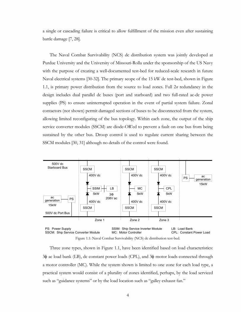
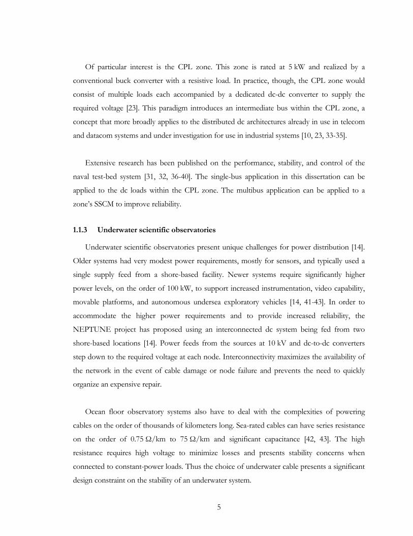
The Naval Combat Survivability (NCS) dc distribution system was jointly developed at
Purdue University and the University of Missouri-Rolla under the sponsorship of the US Navy
with the purpose of creating a well-documented test-bed for reduced-scale research in future
Naval electrical systems [30-32]. The primary scope of the 15 kW dc test-bed, shown in Figure
1.1, is primary power distribution from the source to load zones. Full 2n redundancy in the
design includes dual parallel dc buses (port and starboard) and two full-rated ac-dc power
supplies (PS) to ensure uninterrupted operation in the event of partial system failure. Zonal
contactors (not shown) permit damaged sections of buses to be disconnected from the system,
allowing limited reconfiguring of the bus topology. Within each zone, the output of the ship
service converter modules (SSCM) are diode-OR’ed to prevent a fault on one bus from being
sustained by the other bus. Droop control is used to regulate current sharing between the
SSCM modules [30, 31] although no details of the control were found.
SSIM
SSCM
SSCM
LB
SSCM
SSCM
MC CPL
SSCM
SSCM
PSacgeneration
PS acgeneration
500V dc Port Bus
400V dc
400V dc
3Φ208V ac
400V dc
400V dc
400V dc
400V dc
500V dc Starboard Bus
Zone 1 Zone 2 Zone 3
PS: Power SupplySSCM: Ship Service Converter Module
SSIM: Ship Service Inverter ModuleMC: Motor Controller
LB: Load BankCPL: Constant Power Load
5kW 5kW 5kW
15kW
15kW
Figure 1.1: Naval Combat Survivability (NCS) dc distribution test-bed.
Three zone types, shown in Figure 1.1, have been identified based on load characteristics:
3φ ac load bank (LB), dc constant power loads (CPL), and 3φ motor loads connected through
a motor controller (MC). While the system shown is limited to one zone for each load type, a
practical system would consist of a plurality of zones identified, perhaps, by the load serviced
such as “guidance systems” or by the load location such as “galley exhaust fan.”
5
Of particular interest is the CPL zone. This zone is rated at 5 kW and realized by a
conventional buck converter with a resistive load. In practice, though, the CPL zone would
consist of multiple loads each accompanied by a dedicated dc-dc converter to supply the
required voltage [23]. This paradigm introduces an intermediate bus within the CPL zone, a
concept that more broadly applies to the distributed dc architectures already in use in telecom
and datacom systems and under investigation for use in industrial systems [10, 23, 33-35].
Extensive research has been published on the performance, stability, and control of the
naval test-bed system [31, 32, 36-40]. The single-bus application in this dissertation can be
applied to the dc loads within the CPL zone. The multibus application can be applied to a
zone’s SSCM to improve reliability.
1.1.3 Underwater scientific observatories
Underwater scientific observatories present unique challenges for power distribution [14].
Older systems had very modest power requirements, mostly for sensors, and typically used a
single supply feed from a shore-based facility. Newer systems require significantly higher
power levels, on the order of 100 kW, to support increased instrumentation, video capability,
movable platforms, and autonomous undersea exploratory vehicles [14, 41-43]. In order to
accommodate the higher power requirements and to provide increased reliability, the
NEPTUNE project has proposed using an interconnected dc system being fed from two
shore-based locations [14]. Power feeds from the sources at 10 kV and dc-to-dc converters
step down to the required voltage at each node. Interconnectivity maximizes the availability of
the network in the event of cable damage or node failure and prevents the need to quickly
organize an expensive repair.
Ocean floor observatory systems also have to deal with the complexities of powering
cables on the order of thousands of kilometers long. Sea-rated cables can have series resistance
on the order of 0.75 Ω/km to 75 Ω/km and significant capacitance [42, 43]. The high
resistance requires high voltage to minimize losses and presents stability concerns when
connected to constant-power loads. Thus the choice of underwater cable presents a significant
design constraint on the stability of an underwater system.
6
Emergency control algorithms monitor the power system and apply a hierarchy of priority
to each load based on four classifications shown in Table 1.1 [14]. The priority classification is
useful in the event load-shed becomes necessary to prevent voltage collapse and the order in
which loads are re-energized once the system is capable of supporting increased loading. The
concept of priority-based control is fundamental to the work in this dissertation and is
explored in further detail in later chapters.
Table 1.1: Categories of load priority in the NEPTUNE power system Classification Description
Essential Crucial to safe system operation. They must be kept energized.
High-Priority Important loads. Extra effort is required to keep them energized.
General General purpose loads. No extra effort is required to keep them energized.
Deferrable Candidate loads for shedding as the system approaches peak power.
1.1.4 Spacecraft
Spacecraft contain complete distributed power systems including generation, distribution,
storage and load. Dc systems are extensively used since solar panels, batteries, and typical
payload all are fundamentally dc devices [44]. The distributed design offers numerous
advantages over a centralized design including high reliability, ease of failure containment,
redundancy, controllable power quality for different loads, flexibility, and expandability [45,
46]. The power requirements of spacecraft continue to grow with communication and sensor
spacecraft requiring upwards of 30 kW and space platforms such as the International Space
Station requiring over 100 kW [47]. A significant amount of the literature in spacecraft power
systems is devoted to the small-signal stability of a dc power system [44, 45, 48-51]. Chapter 3
reviews some of the stability criteria that resulted from this work.
The International Space Station (ISS) power system is composed of two relatively
independent dc system with different voltages [20, 21]. The U.S. system runs at 120 V and has
solar power modules with a capacity of 76 kW. The Russian system is divided into 120 V and
28 V components and has 29 kW of solar generation. The two systems are interconnected
with bidirectional dc-dc converters to allow transfer of power based on demand and available

7
supply. The low-earth orbit means that no solar insolation of the panels will occur for a
portion of the 90 min orbital period. During the eclipse, on-board batteries supply the entire
load. Dynamic priority-based load control can help to extend the availability of stored energy
for critical loads if electrical demand increases during the eclipse.
1.1.5 Distributed generation and microgrids
The commercial power industry has traditionally been vertically integrated and centrally
controlled. Deregulation has forced decentralization throughout the industry and mandated
less restrictive access to the power infrastructure and markets, particularly in the area of
distributed generation. While the majority of the bulk power is still produced by large
generation plants with steam turbines and synchronous generators, distributed generation
(DG) has become more attractive. In a DG system, the sources are usually colocated with their
loads. The close proximity to the load allows utilization of waste heat in a combined heat and
electricity cycle that increases the overall energy conversion efficiency [52]. In the past, local
generation was almost exclusively used for stand-alone backup power. Today, distributed
generation is integrated with the commercial power system and can help level peak demands as
well as provide on-line buffering from disturbances on the bulk power grid [53].
A microgrid is a flexible, controllable, interface between local sources of generation and
load and the larger bulk power system [54]. A microgrid with distributed generation and load is
a electrically weak power system; the high effective system impedance makes the system prone
to voltage instability and collapse even though the steady-state power flow may be well below
the available maximum power transfer limit. Constant power loads exacerbate the stability
problem by demanding constant power even if the system is not capable of delivering it. Like
the other dc systems, stability is remains an active are of research for these systems.
Lasseter proposed a dc ring topology for a microgrid, as shown in Figure 1.2, to integrate a
plurality of loads and sources and support one topological failure [11]. Multiple local sources
including standby generation and alternative energy sources augment the feed from the larger
ac grid to supply a variety of load types. Rectifiers provide the interface between ac sources
and the dc bus, inverters convert the dc bus into ac voltage for ac loads, and dc-dc converters
connect dc sources and loads with different voltages to the bus. The dc bus facilitates
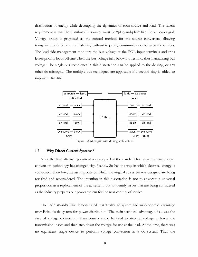
8
distribution of energy while decoupling the dynamics of each source and load. The salient
requirement is that the distributed resources must be “plug-and-play” like the ac power grid.
Voltage droop is proposed as the control method for the source converters, allowing
transparent control of current sharing without requiring communication between the sources.
The load-side management monitors the bus voltage at the POL input terminals and trips
lesser-priority loads off-line when the bus voltage falls below a threshold, thus maintaining bus
voltage. The single-bus techniques in this dissertation can be applied to the dc ring, or any
other dc microgrid. The multiple bus techniques are applicable if a second ring is added to
improve reliability.
Figure 1.2: Microgrid with dc ring architecture.
1.2 Why Direct Current Systems?
Since the time alternating current was adopted at the standard for power systems, power
conversion technology has changed significantly. So has the way in which electrical energy is
consumed. Therefore, the assumptions on which the original ac system was designed are being
revisited and reconsidered. The intention in this dissertation is not to advocate a universal
proposition as a replacement of the ac system, but to identify issues that are being considered
as the industry prepares our power system for the next century of service.
The 1893 World’s Fair demonstrated that Tesla’s ac system had an economic advantage
over Edison’s dc system for power distribution. The main technical advantage of ac was the
ease of voltage conversion. Transformers could be used to step up voltage to lower the
transmission losses and then step down the voltage for use at the load. At the time, there was
no equivalent single device to perform voltage conversion in a dc system. Thus the

9
Westinghouse backed ac system became the standard for generation, transmission,
distribution, and consumption of electrical energy.
In the early twentieth century, the loads were incandescent lamps and induction motors
and the sources were synchronous generators. As society’s dependence on electrical energy
increased, the ac grid became ubiquitous and the power industry ballooned. Recent
deregulation has encouraged creative financing and market gaming that seems to have placed
reliability and profitability as contentious goals [55]. In the process, the grid infrastructure has
continued to age and new generation, transmission, and distribution have been insufficient to
keep pace with increasing demand [56, 57].
The widespread blackout of the U.S. Northeast on August 14, 2003, was widely reported
in the popular media and served as a reminder of society’s dependence on electrical power.
The lay press, accustomed to reporting advances in information technology, was befuddled by
this catastrophe and issued a wakeup call for significant innovation in power grid technology
[58-60]. However, experts seemed less astonished and suggested that the size and complexity
of the power grid make blackouts inevitable [61, 62]. Others have begun to question the
benefits of deregulation and the impact of the 2005 Energy Bill on ensuring the reliability of
our commercial power grid [63].
Although the blackout seized public attention and suggested that the industry had fallen
behind present day needs, outside of the public view there are vibrant research and
development efforts. Advances in the understanding of dynamic stability and improvements in
network visualization are two examples of new analytical and design tools. Older technology is
being replaced by power electronics in applications such as reactive power compensation,
motor drives, and point-of-use energy conversion [64]. Alternative energy sources like
photovoltaic and fuel cells are becoming economically feasible due to tremendous progress in
material sciences.
However, modern loads are fundamentally different from early twentieth century loads.
Three-phase ac motors delivering torque to the factory are being replaced by computers
processing numbers in data centers [56]. Where motors are used, line-start induction machines

10
are being replaced by motor-drive pairs that increase the efficiency and performance while
reducing size, weight, and cost [65, 66]. Although lighting still represents a large portion of the
load, tungsten filament lamps are increasingly being replaced by higher efficiency fluorescent
lamps with electronic ballasts. Solid state, high-efficiency light emitting diodes (LED) will likely
render incandescent lamps obsolete [67]. All of these new loads fundamentally favor direct
current power systems since they require that 60 Hz ac be rectified and filtered before the
power is in usable form.
The demand for premium power is increasing in all areas of commerce. Industrial
processes are becoming increasingly sensitive to power quality [57]. Service-oriented sectors,
such as financial services, rely on communications and data networks as the backbone of their
enterprise. Transients lasting only milliseconds can result in the shutdown of entire production
facilities and data server outages [4, 68, 69]. According to a report by EPRI, the existing power
infrastructure is not sufficient to deliver the increasing demand for high-quality, “digital-
grade,” power for reliable operation of these digital devices [57].
Distributed generation (DG) from both renewable and nonrenewable sources has been
shown to improve the reliability of the grid and can help provide premium power [70]. Experts
suggest, however, that too much may cause stability problems for the ac system [70-73] and
require conditioning with power electronics [52, 53] or interconnection through a dc system
[74]. Integrating nonrenewable generation into the distribution system is a way to increase the
effective capacity of the transmission system and provide premium power to locally connected
loads [75]. It can also improve the efficiency of generation because waste heat can be used for
additional electrical generation in a combined-cycle power plant or as a source of thermal
energy in a cogeneration plant [52]. Renewable energy and green energy sources such as wind,
solar, fuel cells, and geothermal are likely to become widespread in the future due to
environmental regulations and the diminishing supply of fossil fuels [76]. Many of these
sources do not produce first-power at line voltage and frequency. A dc system facilitates the
interconnection of these sources and energy storage to improve the reliability and availability
of the system [12, 13, 74].

11
Originally, many buildings in urban areas such as Manhattan, NY, were equipped with dc
electrical systems that have since been converter to ac [77]. Recently there has been renewed
interest in distributing dc inside buildings [78-80]. Proponents cite the increasing demand for
dc power by electronic devices and sensitive loads as well as the desire to move backup power
from UPS systems powering individual loads to system wide centralized backup power [80]. A
recent study by Lawrence Berkeley National Laboratory found that office and network
equipment directly use 74 TWh of electricity [81]. The total energy consumption is much larger
when the heat load is considered.
Power dissipated in electronic equipment places a cooling burden on HVAC equipment,
particularly during summer months when electricity demand is already high. The heat load of
the electrical equipment can be computed from the coefficient of performance (COP) for the
cooling system:
cooling
loadP
PCOP = (1.1)
The lower limit for the COP of a vapor compression cycle HVAC system, found in most
office buildings, is 2.5 [82]. This means that 40 W of electricity are consumed to remove
100 W dissipated by an electrical load. Therefore, an improvement in electrical conversion
efficiency of even just a few percent will have a significant impact on total energy demand.
As the number of modern sources and loads connected in a distribution system increases,
it is useful to reevaluate system integration. Figure 1.3 is an example of a distribution system in
a modern commercial building. The system is primarily supplied from the commercial ac grid
but has been augmented with additional sources for backup, green, or economic operation.
Alternative energy sources which produce dc electricity, such as fuel cells and solar panels
require an inverter to connect them to the ac grid. Natural gas microturbines, which rotate at
high speed, require energy conversion to be grid compatible. On the load side, most new loads
are either fundamentally dc or require one or more conversion steps with a dc link. The
implication is that there are a number of redundant energy conversion steps cascaded between
the energy source and the energy load. In the case of a computer with a UPS, if the electricity
used is generated by an alternative energy source, there are likely to be five or more energy
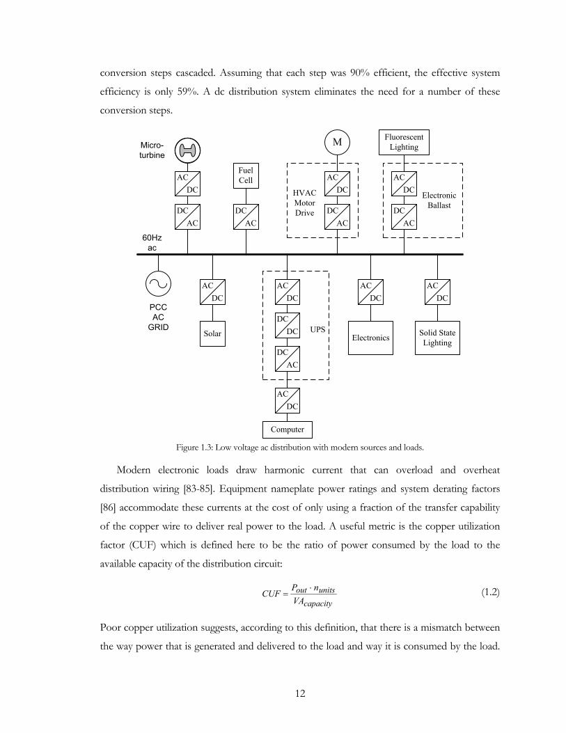
12
conversion steps cascaded. Assuming that each step was 90% efficient, the effective system
efficiency is only 59%. A dc distribution system eliminates the need for a number of these
conversion steps.
Electronics
FuelCell
Solar
ACDC
DCAC
ACDC
DCAC
ACDC
M
ACDC
DCAC
ACDC
DCDC
Computer
UPS
HVACMotor Drive
FluorescentLighting
DCAC
Micro-turbine
PCCAC
GRID
DCAC
ACDC
ACDC
ElectronicBallast
Solid StateLighting
ACDC
60Hz ac
Figure 1.3: Low voltage ac distribution with modern sources and loads.
Modern electronic loads draw harmonic current that can overload and overheat
distribution wiring [83-85]. Equipment nameplate power ratings and system derating factors
[86] accommodate these currents at the cost of only using a fraction of the transfer capability
of the copper wire to deliver real power to the load. A useful metric is the copper utilization
factor (CUF) which is defined here to be the ratio of power consumed by the load to the
available capacity of the distribution circuit:
capacity
unitsoutVA
nPCUF
⋅= (1.2)
Poor copper utilization suggests, according to this definition, that there is a mismatch between
the way power that is generated and delivered to the load and way it is consumed by the load.
13
There are well-known techniques that act as an interface between the dc electronic loads and
the ac system [87, 88] but they require additional conversion stages which increase the size,
weight, and cost of the point-of-load converter.
In summary, this section has presented some of the evolutionary changes that have
occurred in our power system since ac was adopted as the standard. These issues give reason
to consider dc for advanced energy systems. This dissertation only examines dc applications
for autonomous local control.
1.3 Controls to Improve Reliability
In many power systems, matching the supply with the demand to ensure stable and reliable
operation is a nontrivial control problem. The task is further complicated if the power system
becomes energy constrained, that is, there is either insufficient supply or insufficient
distribution to deliver it to the load. Many of the applications where dc is used, such as
shipboard and spacecraft systems, are finite energy systems. Without the ability to connect to
auxiliary sources of energy, they may continually operate near the threshold of being energy
constrained. Considering the load as an actuator instead of a disturbance presents new control
possibilities that can increase the reliability of such a power system [89-92].
Relying on the load to be a participant in system stability requires a control system that is
fault tolerant and self-healing. Fault-tolerant controls can survive partial loss or malfunction of
system components [93]. Self-healing controls take action to abate further disruption and
ensure that the remaining components can operate as best as possible [94-96]. These two
qualities are critical since the power system may be required to continue to operate under
external attack, such as in a Naval application, or unmanned such as on spacecraft or undersea.
This dissertation considers both supply-side and load-side management strategies in a
distributed dc system. On the supply side, droop control will be used to share current among
multiple sources, add system damping to improve dynamic performance, and provide system
wide information in the form of the bus voltage. On the load side, bus selection will be
explored in a multibus system. Dynamic load interruption will be used when load shed
becomes necessary. Autonomous local controllers implement the supply-side and load-side
14
management. They use locally obtained information in the form of the bus voltage and can
operate without requiring a central control or peer-to-peer communication. These controls are
fault tolerant; there is no single point of failure and if one malfunctions the others can
continue to operate. They are also self-healing; important loads remain powered, while less
important loads act to prevent cascading system failure.
1.3.1 Droop control
Droop control has been proposed in the literature as a way to share current when multiple
sources feed a single bus [97-100]. Since this is done by adjusting the output impedance of the
converters, droop control will be shown to be useful to control system damping. A drop in
bus voltage, whether due to partial loss of generation or the need to stabilize the system,
conveys information comparable to what frequency does in an ac system [101]. Load-side
controls that can sense this drop in voltage may take steps to improve system security.
1.3.2 Dynamic load interruption
In the terrestrial ac grid literature, load shedding is often perceived as an undesirable event
and usually reserved for emergency conditions where damage to power generation equipment
and cascading blackouts are likely [91, 102]. Some utilities have interruptible contracts with
large industrial customers and use load shed to curtail load during peak demands [103]. The
load-shed is initiated from a central dispatch location. Recent work has reexamined the role of
interruptible loads in the power system [90, 104]. Automating the load-shed process and
incorporating power electronic methods increase the actuation time to less than a single line-
cycle. It has been reported that automatic, dynamically interruptible loads offer an alternative
to building more generation [103-105]. As interruptible load transitions from a static load-
leveling [106] into a dynamic security technique [104, 107], additional benefit can be gained by
considering the residential energy market [91, 108, 109].
A more interesting aspect load shed is load restoration, a topic not well represented in the
literature. Turning on a previously shed load can introduce additional perturbations in the
system. The result could be reshedding of the same load or shedding of other loads. An
undesirable effect would be the interruption of critical loads when less important loads attempt
15
to re-energize. The objective of the restoration process is to maximize the number of loads
supplied without violating system constraints [110].
1.3.3 Bus selection
Multiple supply buses can increase the reliability of a power system by providing multiple
configuration options for supplying power to the load. The load can operate from both buses
simultaneously or operate from a preferred bus and have others available as backup feeds.
Choosing the best bus from which to operate requires either a contingency power flow
analysis or a perturb-and-observe switching strategy. The former is possible in a central control
system. The latter is required if the system is completely distributed using only local
information.
1.3.4 Load priority
In an energy constrained system, load priority is critical for system stability and control
because it provides a structure approach to the decision and control process [11, 111, 112].
When the system becomes energy constrained and load shed becomes necessary, load priority
allows important loads to remain energized at the expense of less important loads [14].
Depending on the system, priority can be assigned on a circuit by circuit basis or at each
individual load. A flexible control strategy is needed since it is possible that the priority of a
particular load can dynamically change.
1.4 Common Control Structures
Control schemes in power systems can be described in terms of architecture and process.
The architecture refers to the location and structure of the control system and spans the range
from centralized to distributed. In a centralized architecture, measurements and sensor signals
return to a common location where control action for the entire system is determined.
Actuation signals disseminate out into the system. The control objectives and optimization
functions can be changed easily. The local control architecture places the controls at the point
of sensing and actuation. It offers a lower installation cost than centralized control, faster
response time, and increased reliability since it does not rely on communication [102].
16
The control process can be rule-based, algorithmic, or behavioral [102]. Rule-based
controls are technologically simpler to implement but require the expert knowledge of the
designer and specific knowledge of the system to be controlled [102]. Thus a rule-based system
may not be flexible enough to accommodate system operation and reconfiguration beyond
what was foreseen in the original design. Algorithmic controls are more complicated but are
better suited when flexibility is important. Some examples of algorithmic controls are adaptive
controls, genetic algorithms, and neural networks [110]. Rule-based and algorithmic controls
are reactive in nature in that they associate sensory input with specific actuation. Behavioral
control is governed by a set of objectives and a set of constraints and is not limited in the way
it can react to a system. Like the algorithmic controls, behavioral controls generally require an
accurate model of the system in order to determine the best course of action.
The work in this dissertation investigates rule-based local controls. It is left as future work
to refine the strategies presented here by applying more sophisticated algorithmic or behavioral
local control techniques.
1.4.1 Centralized control
In a centralized control system, a controller interacts with multiple entities in the
environment. Sensor information and actuation signals are home-run from the entity to the
controller, as shown in Figure 1.4. Thus each entity is fully observable and controllable.
Centralized control schemes are well suited for difficult optimization problems, such as
economic operation, that require system-level coordination. In general, the control objectives
and optimization functions can easily be changed to match operational requirements of the
system. Physical distance and conditions of the communication link can limit the ability of the
central controller to react quickly. In the absence of complete system knowledge the controller
can use a state-estimator to approximate the condition of the system, a common practice by
the commercial power utilities. However, analysis of the 2003 blackout suggests that a
centralized control scheme can be inadequate in an emergency situation, particularly if the
system is undersensed since the state estimators can provide misleading information about the
actual state of the system.
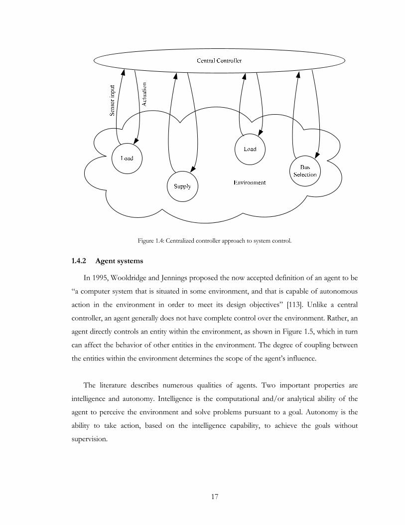
17
Figure 1.4: Centralized controller approach to system control.
1.4.2 Agent systems
In 1995, Wooldridge and Jennings proposed the now accepted definition of an agent to be
“a computer system that is situated in some environment, and that is capable of autonomous
action in the environment in order to meet its design objectives” [113]. Unlike a central
controller, an agent generally does not have complete control over the environment. Rather, an
agent directly controls an entity within the environment, as shown in Figure 1.5, which in turn
can affect the behavior of other entities in the environment. The degree of coupling between
the entities within the environment determines the scope of the agent’s influence.
The literature describes numerous qualities of agents. Two important properties are
intelligence and autonomy. Intelligence is the computational and/or analytical ability of the
agent to perceive the environment and solve problems pursuant to a goal. Autonomy is the
ability to take action, based on the intelligence capability, to achieve the goals without
supervision.
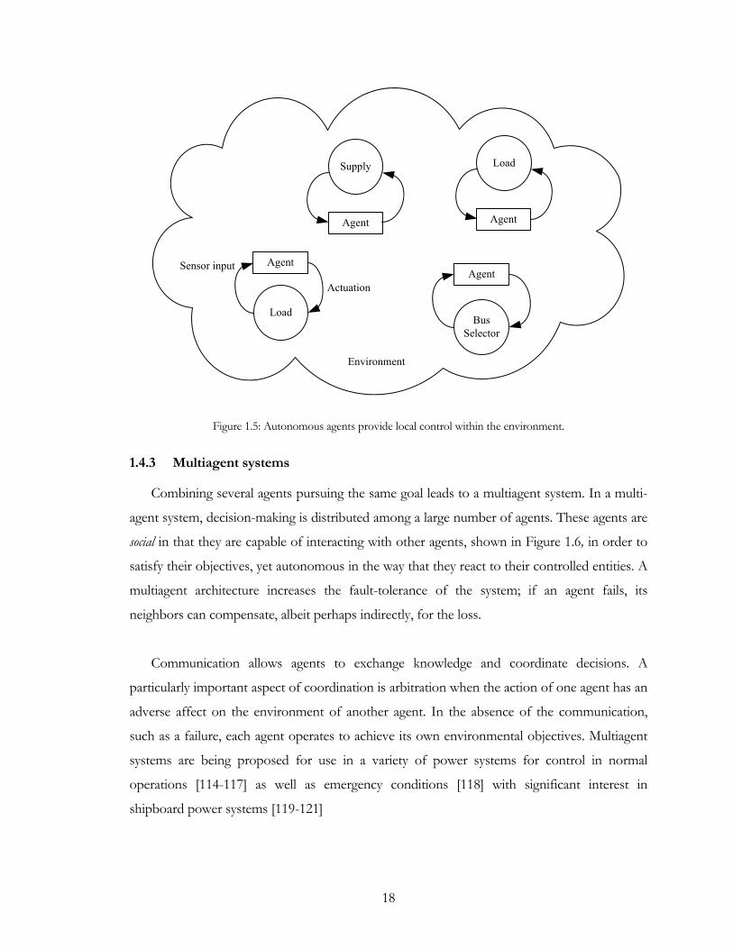
18
Supply Load
Bus Selector
Load
Agent
Agent
Agent
Agent
Actuation
Sensor input
Environment
Figure 1.5: Autonomous agents provide local control within the environment.
1.4.3 Multiagent systems
Combining several agents pursuing the same goal leads to a multiagent system. In a multi-
agent system, decision-making is distributed among a large number of agents. These agents are
social in that they are capable of interacting with other agents, shown in Figure 1.6, in order to
satisfy their objectives, yet autonomous in the way that they react to their controlled entities. A
multiagent architecture increases the fault-tolerance of the system; if an agent fails, its
neighbors can compensate, albeit perhaps indirectly, for the loss.
Communication allows agents to exchange knowledge and coordinate decisions. A
particularly important aspect of coordination is arbitration when the action of one agent has an
adverse affect on the environment of another agent. In the absence of the communication,
such as a failure, each agent operates to achieve its own environmental objectives. Multiagent
systems are being proposed for use in a variety of power systems for control in normal
operations [114-117] as well as emergency conditions [118] with significant interest in
shipboard power systems [119-121]
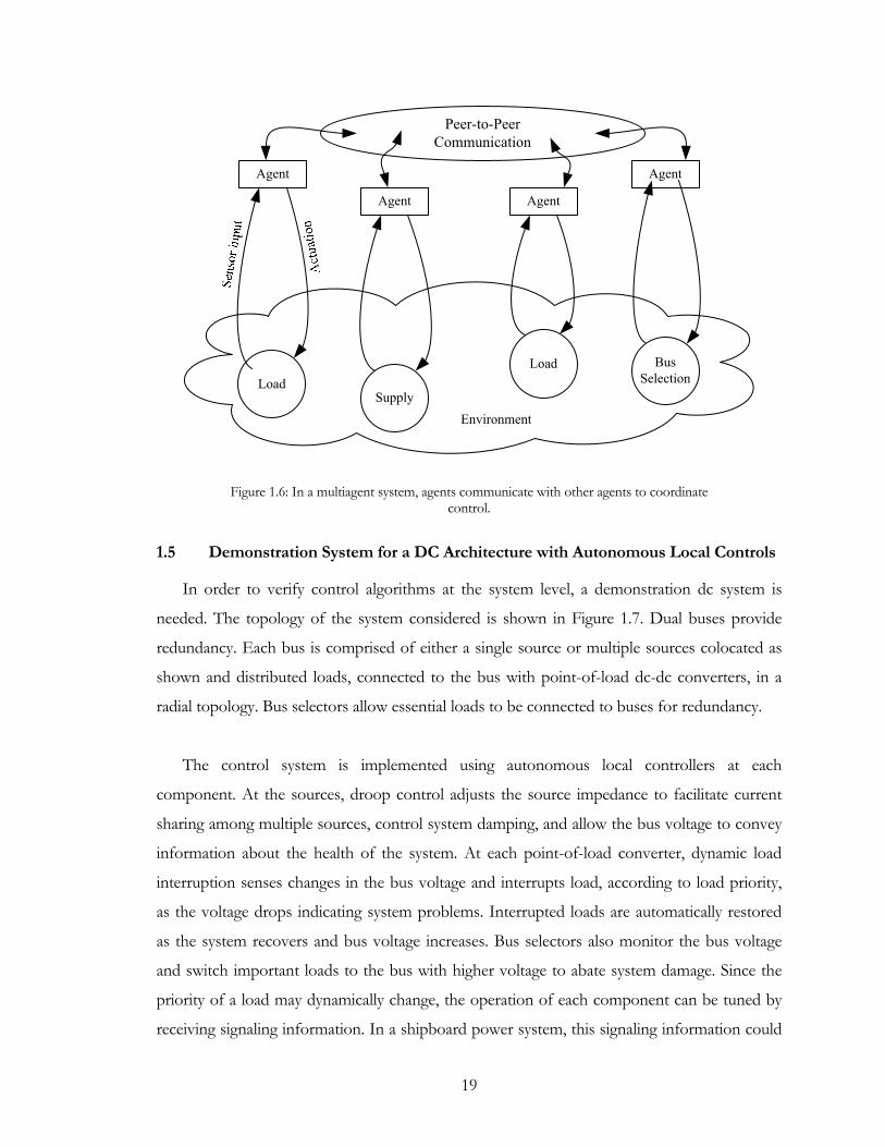
19
Peer-to-PeerCommunication
Supply
Agent
Load
Agent
Load
Agent
BusSelection
Agent
Environment
Figure 1.6: In a multiagent system, agents communicate with other agents to coordinate control.
1.5 Demonstration System for a DC Architecture with Autonomous Local Controls
In order to verify control algorithms at the system level, a demonstration dc system is
needed. The topology of the system considered is shown in Figure 1.7. Dual buses provide
redundancy. Each bus is comprised of either a single source or multiple sources colocated as
shown and distributed loads, connected to the bus with point-of-load dc-dc converters, in a
radial topology. Bus selectors allow essential loads to be connected to buses for redundancy.
The control system is implemented using autonomous local controllers at each
component. At the sources, droop control adjusts the source impedance to facilitate current
sharing among multiple sources, control system damping, and allow the bus voltage to convey
information about the health of the system. At each point-of-load converter, dynamic load
interruption senses changes in the bus voltage and interrupts load, according to load priority,
as the voltage drops indicating system problems. Interrupted loads are automatically restored
as the system recovers and bus voltage increases. Bus selectors also monitor the bus voltage
and switch important loads to the bus with higher voltage to abate system damage. Since the
priority of a load may dynamically change, the operation of each component can be tuned by
receiving signaling information. In a shipboard power system, this signaling information could
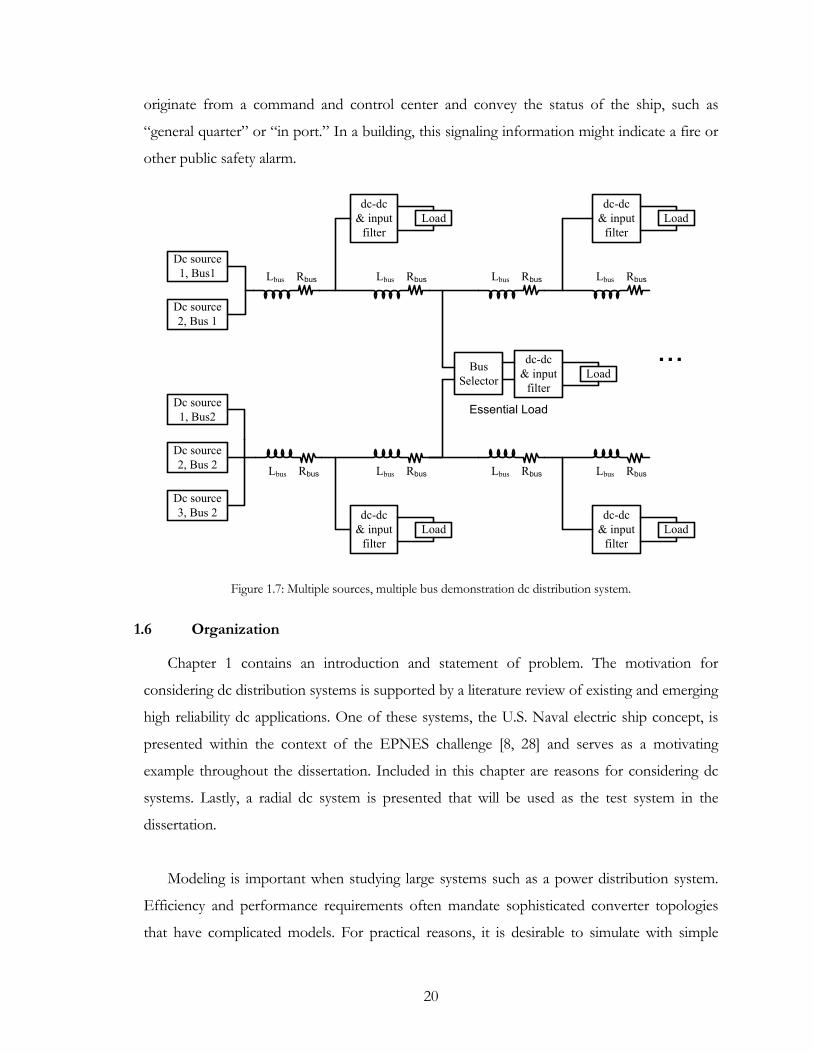
20
originate from a command and control center and convey the status of the ship, such as
“general quarter” or “in port.” In a building, this signaling information might indicate a fire or
other public safety alarm.
Essential Load
BusSelector
dc-dc & input
filterLoad
Dc source 1, Bus1 RbusLbus RbusLbus
dc-dc & input
filterLoad
RbusLbus RbusLbus
dc-dc & input
filterLoad
RbusLbus RbusLbus
dc-dc & input
filterLoad
RbusLbus RbusLbus
dc-dc & input
filterLoad
Dc source 2, Bus 1
Dc source 1, Bus2
Dc source 2, Bus 2
Dc source 3, Bus 2
Figure 1.7: Multiple sources, multiple bus demonstration dc distribution system.
1.6 Organization
Chapter 1 contains an introduction and statement of problem. The motivation for
considering dc distribution systems is supported by a literature review of existing and emerging
high reliability dc applications. One of these systems, the U.S. Naval electric ship concept, is
presented within the context of the EPNES challenge [8, 28] and serves as a motivating
example throughout the dissertation. Included in this chapter are reasons for considering dc
systems. Lastly, a radial dc system is presented that will be used as the test system in the
dissertation.
Modeling is important when studying large systems such as a power distribution system.
Efficiency and performance requirements often mandate sophisticated converter topologies
that have complicated models. For practical reasons, it is desirable to simulate with simple

21
models and prototype at reduced power levels. Chapter 2 discusses reduced-order and
reduced-power modeling of converters that preserve small-signal characteristics.
The interconnection of a large number of high-bandwidth nonlinear dc power converters
remains an area of active research [9, 122]. The constant-power behavior of dc-dc converters
results in negative dynamic input resistance and can have a destabilizing effect on the system
[123]. Maximum power transfer capability, straightforward with resistive loads, is complicated
by constant-power loads. The small-signal interaction between the negative dynamic
impedance of the power converter, its input filter, and the dc distribution system presents well-
known stability concerns. Chapter 3 explores the origins of instability in a dc system and
reviews the small-signal criteria that have been proposed in the literature.
Chapter 4 develops the concept of autonomous local control as the central theme of this
thesis. Local control, using locally sensed information, is presented as a control strategy that
does not require a centralized controller to coordinate system operation but that promotes
system stability. Load priority is used to integrate a power buffer with new load-side control
techniques.
Chapter 5 demonstrates a single-bus application for both the supply and load. Droop
control, a local control technique for power sources, is shown to have a global small-signal
stabilizing effect on the system, a result not previously explored in the literature. On the load
side, intelligent dynamic load switching is presented as a local control that stabilizes the system
by reducing demand. A challenge in implementing dynamic load switching is to determine the
values for the undervoltage and load-restoration set points. An algorithm based on an
exhaustive load-flow analysis is presented for the test system. The problem is then generalized
as a multilevel integer program suitable for arbitrary systems. Dynamic load control changes
the effective system impedance. Monitoring the system impedance will be presented as an on-
line technique to initiate dynamic load control. Experimental verification demonstrates load
interruption according to priority.
Local controls can be used in a multiple bus system to promote systemwide stability and
reliability. Chapter 6 examines methods for connecting a point-of-load converter to multiple

22
supply buses. ORing diodes, commonly used, provide smooth crossover from one bus to
another but present an ill-defined operating state when the bus voltages are similar. Two
alternative methods are presented. In the first, controlled switches replace the diodes and allow
carefully orchestrated bus switching. Concepts from hybrid switched-system theory are applied
to ensure stable switching. Active switching introduces discontinuous current onto the buses.
This can be undesirable for some applications where interference or electromagnetic signature
is a concern. A second solution is proposed that uses auctioneering diodes combined with bus
converters. The diodes ensure continuous current and fail-safe operation and the bus
converter programs the exact profile for bus switching.
Conclusions are summarized in Chapter 7 along with a discussion of potential future work
in this area.
In this work, significant emphasis has been placed on design and reduction to practice. To
that end, extensive custom hardware was designed by the author and fabricated with the help
of undergraduate laboratory assistants. Appendix A provides design details for the analog
closed-loop dc-dc converter and digital supervisor that implemented the autonomous local
controller. Schematics and printed circuit board (PCB) artwork are shown for the converter
and controller. A thorough analysis of the buck converter including derivation of small-signal
transfer functions and closed-loop properties is presented along with experimental
performance data. Firmware and operational details are provided for the digital controller.
Appendix B provides the MATLAB implementation of the search algorithm from Chapter 5
to find the undervoltage load-interruption and load-restoration voltage set points.
Portions of Chapter 4 and 5 of this dissertation have been previously published [124, 125].

23
CHAPTER 2 MODELING
Analysis of high-order, nonlinear, systems requires good modeling. In a dc system, there
are a number of phenomena that of are interest and each requires different modeling
techniques. In this dissertation, it is assumed that the characteristics of each individual
converter, including closed-loop operation, are known and properly designed to be
independently stable and meet certain performance objectives. The focus in this work is on the
interaction of a system of dc-dc converters. The first section in this chapter defines an abstract
model for the system-level control and operation of a generic power converter. Since
subsequent chapters will discuss control techniques, it is important to define the scope of these
control actions.
The interaction of converters with each other and the distribution bus involves both small-
signal and large-signal effects. A common technique when analyzing these small-signal
interactions is to obtain the small-signal transfer functions [126-128]. Since these transfer
functions depend on component parameters such as inductance and capacitance as well as the
operating point of the converter, it is difficult to generalize the converter operation to other
power levels and operating points. This becomes important since, for practical reasons, it is
desirable to experiment with low-power and smaller systems. While results published in the
literature are often obtained from reduced-scale prototypes [30], there is seldom an attempt in
the literature to correlate the performance of the prototype system to the full-scale system. The
remainder of the chapter investigates techniques for deriving scaled models, suitable for
prototype experimentation, that retain the significant small-signal characteristics of their full-
scale equivalents.
2.1 Controller Model
In a dc system, there can be a number of controllers each designed and dedicated to
perform a certain control objective. At each load there is a controller to regulate the closed-
loop performance of the individual converter, such as in voltage mode control. Sources have
similar controls to ensure that the prescribed output voltage is regulated. At the system level,
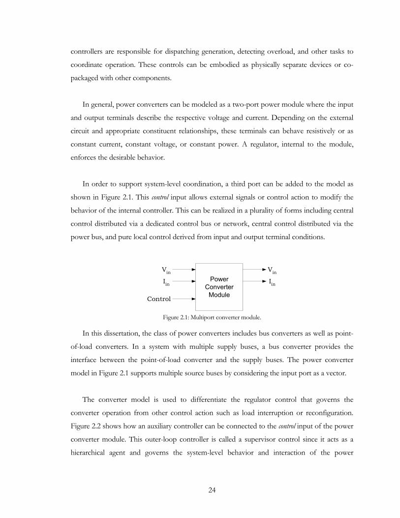
24
controllers are responsible for dispatching generation, detecting overload, and other tasks to
coordinate operation. These controls can be embodied as physically separate devices or co-
packaged with other components.
In general, power converters can be modeled as a two-port power module where the input
and output terminals describe the respective voltage and current. Depending on the external
circuit and appropriate constituent relationships, these terminals can behave resistively or as
constant current, constant voltage, or constant power. A regulator, internal to the module,
enforces the desirable behavior.
In order to support system-level coordination, a third port can be added to the model as
shown in Figure 2.1. This control input allows external signals or control action to modify the
behavior of the internal controller. This can be realized in a plurality of forms including central
control distributed via a dedicated control bus or network, central control distributed via the
power bus, and pure local control derived from input and output terminal conditions.
VinIin
Control
VinIin
PowerConverterModule
Figure 2.1: Multiport converter module.
In this dissertation, the class of power converters includes bus converters as well as point-
of-load converters. In a system with multiple supply buses, a bus converter provides the
interface between the point-of-load converter and the supply buses. The power converter
model in Figure 2.1 supports multiple source buses by considering the input port as a vector.
The converter model is used to differentiate the regulator control that governs the
converter operation from other control action such as load interruption or reconfiguration.
Figure 2.2 shows how an auxiliary controller can be connected to the control input of the power
converter module. This outer-loop controller is called a supervisor control since it acts as a
hierarchical agent and governs the system-level behavior and interaction of the power
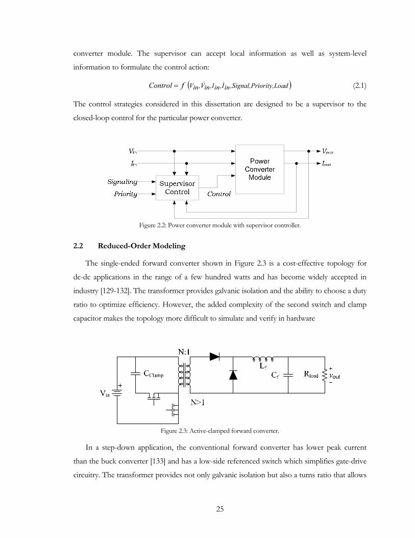
25
converter module. The supervisor can accept local information as well as system-level
information to formulate the control action:
( )diority,Loa,Signal,PrinI,in,IinV,inVfControl &&= (2.1)
The control strategies considered in this dissertation are designed to be a supervisor to the
closed-loop control for the particular power converter.
Figure 2.2: Power converter module with supervisor controller.
2.2 Reduced-Order Modeling
The single-ended forward converter shown in Figure 2.3 is a cost-effective topology for
dc-dc applications in the range of a few hundred watts and has become widely accepted in
industry [129-132]. The transformer provides galvanic isolation and the ability to choose a duty
ratio to optimize efficiency. However, the added complexity of the second switch and clamp
capacitor makes the topology more difficult to simulate and verify in hardware
Figure 2.3: Active-clamped forward converter.
In a step-down application, the conventional forward converter has lower peak current
than the buck converter [133] and has a low-side referenced switch which simplifies gate-drive
circuitry. The transformer provides not only galvanic isolation but also a turns ratio that allows
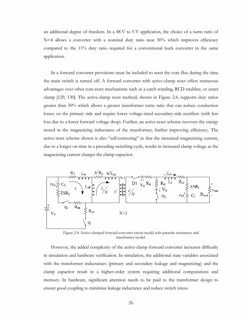
26
an additional degree of freedom. In a 48 V to 5 V application, the choice of a turns ratio of
N=4 allows a converter with a nominal duty ratio near 50% which improves efficiency
compared to the 11% duty ratio required for a conventional buck converter in the same
application.
In a forward converter provisions must be included to reset the core flux during the time
the main switch is turned off. A forward converter with active-clamp reset offers numerous
advantages over other core-reset mechanisms such as a catch-winding, RCD snubber, or zener
clamp [129, 130]. The active-clamp reset method, shown in Figure 2.4, supports duty ratios
greater than 50% which allows a greater transformer turns ratio that can reduce conduction
losses on the primary side and require lower voltage-rated secondary-side rectifiers (with less
loss due to a lower forward voltage drop). Further, an active-reset scheme recovers the energy
stored in the magnetizing inductance of the transformer, further improving efficiency. The
active-reset scheme shown is also “self-correcting” in that the increased magnetizing current,
due to a longer on-time in a preceding switching cycle, results in increased clamp voltage as the
magnetizing current charges the clamp capacitor.
Ni21i
Nv′v′
Figure 2.4: Active-clamped forward converter circuit model with parasitic resistances and
transformer model.
However, the added complexity of the active-clamp forward converter increases difficulty
in simulation and hardware verification. In simulation, the additional state variables associated
with the transformer inductances (primary and secondary leakage and magnetizing) and the
clamp capacitor result in a higher-order system requiring additional computations and
memory. In hardware, significant attention needs to be paid to the transformer design to
ensure good coupling to minimize leakage inductance and reduce switch stress.
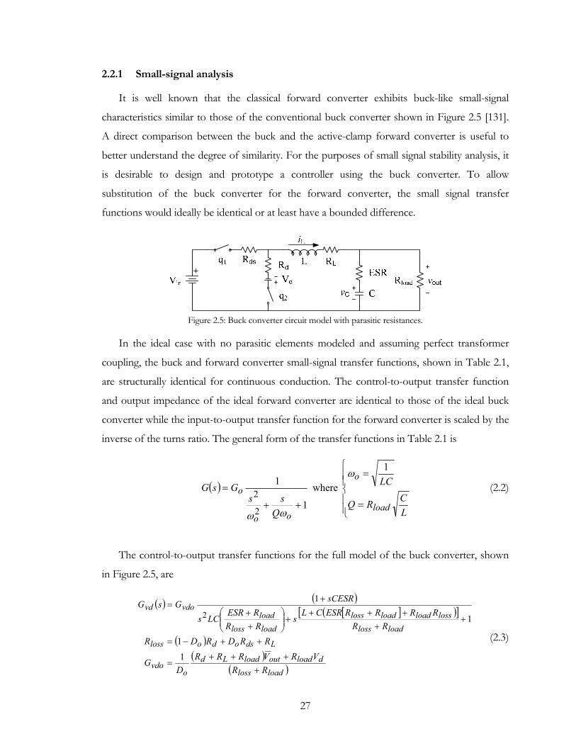
27
2.2.1 Small-signal analysis
It is well known that the classical forward converter exhibits buck-like small-signal
characteristics similar to those of the conventional buck converter shown in Figure 2.5 [131].
A direct comparison between the buck and the active-clamp forward converter is useful to
better understand the degree of similarity. For the purposes of small signal stability analysis, it
is desirable to design and prototype a controller using the buck converter. To allow
substitution of the buck converter for the forward converter, the small signal transfer
functions would ideally be identical or at least have a bounded difference.
Figure 2.5: Buck converter circuit model with parasitic resistances.
In the ideal case with no parasitic elements modeled and assuming perfect transformer
coupling, the buck and forward converter small-signal transfer functions, shown in Table 2.1,
are structurally identical for continuous conduction. The control-to-output transfer function
and output impedance of the ideal forward converter are identical to those of the ideal buck
converter while the input-to-output transfer function for the forward converter is scaled by the
inverse of the turns ratio. The general form of the transfer functions in Table 2.1 is
( )
⎪⎪⎩
⎪⎪⎨
⎧
=
=
++
=
LCRQ
LC
Qss
GsG
load
o
oo
o
1
where
1
1
2
2
ω
ωω
(2.2)
The control-to-output transfer functions for the full model of the buck converter, shown
in Figure 2.5, are
( ) ( )[ ]( )[ ]
( )( )
( )loadlossdloadoutloadLd
ovdo
Ldsodoloss
loadlosslossloadloadloss
loadlossload
vdovd
RRVRVRRR
DG
RRDRDRRR
RRRRESRCLs
RRRESR
LCs
sCESRGsG
++++
=
++−=
++
++++⎟⎟
⎠
⎞⎜⎜⎝
⎛++
+=
1
1
1
1
2
(2.3)
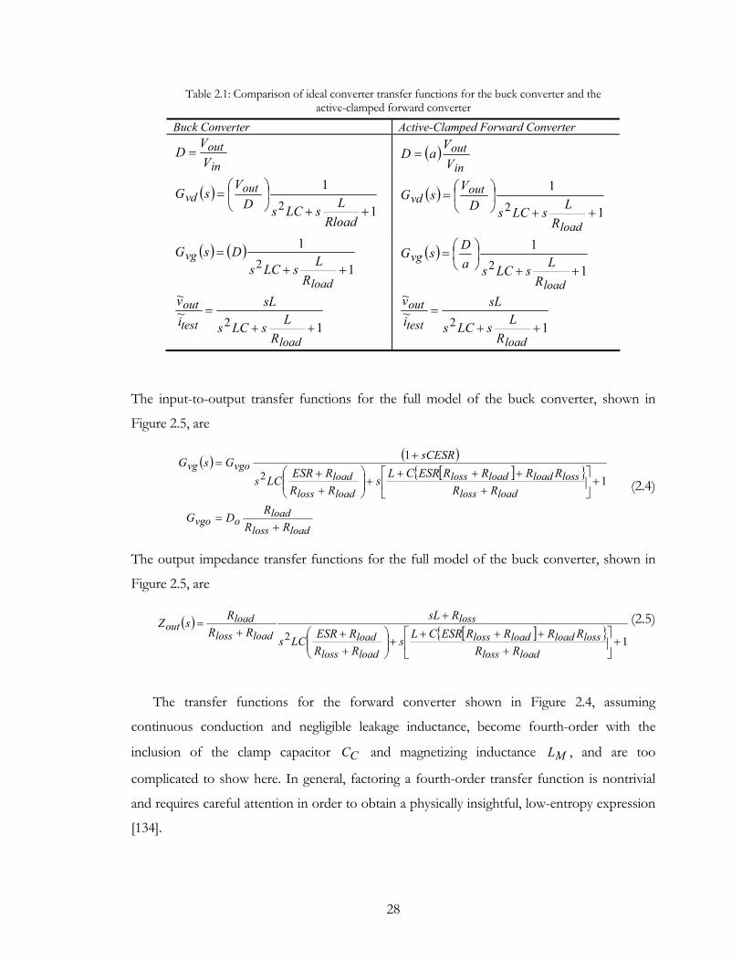
28
Table 2.1: Comparison of ideal converter transfer functions for the buck converter and the active-clamped forward converter
Buck Converter Active-Clamped Forward Converter
inout
VV
D = ( )in
outVV
aD =
( )1
12 ++
⎟⎠
⎞⎜⎝
⎛=
RloadLsLCsD
VsG out
vd ( )1
12 ++
⎟⎠
⎞⎜⎝
⎛=
load
outvd
RLsLCsD
VsG
( ) ( )1
12 ++
=
load
vg
RLsLCs
DsG ( )1
12 ++
⎟⎠⎞
⎜⎝⎛=
load
vg
RLsLCsa
DsG
1~~
2 ++=
loadtest
out
RLsLCs
sLiv
1
~~
2 ++=
loadtest
out
RLsLCs
sLiv
The input-to-output transfer functions for the full model of the buck converter, shown in
Figure 2.5, are
( ) ( )[ ]
loadlossload
ovgo
loadlosslossloadloadloss
loadlossload
vgovg
RRR
DG
RRRRRRESRCL
sRRRESR
LCs
sCESRGsG
+=
+⎥⎦
⎤⎢⎣
⎡+
++++⎟⎟
⎠
⎞⎜⎜⎝
⎛++
+=
1
1
2 (2.4)
The output impedance transfer functions for the full model of the buck converter, shown in
Figure 2.5, are
( )[ ]
12 +⎥⎦
⎤⎢⎣
⎡+
++++⎟⎟
⎠
⎞⎜⎜⎝
⎛++
++
=
loadlosslossloadloadloss
loadlossload
lossloadloss
loadout
RRRRRRESRCL
sRRRESR
LCs
RsLRR
RsZ (2.5)
The transfer functions for the forward converter shown in Figure 2.4, assuming
continuous conduction and negligible leakage inductance, become fourth-order with the
inclusion of the clamp capacitor CC and magnetizing inductance ML , and are too
complicated to show here. In general, factoring a fourth-order transfer function is nontrivial
and requires careful attention in order to obtain a physically insightful, low-entropy expression
[134].
29
Choosing the same duty ratio and output voltage for the buck and forward converter
results in transfer functions that appear reasonably similar. However, without the transformer
turns ratio, the input voltage for the buck converter must be lower than that for the forward
converter and is found to be
( )a
VVVV
VVa inFWD
inBUCKinBUCK
outBUCKinFWD
outFWD =⇒= (2.6)
The choice to operate at the same output voltage and duty ratio preserves the output power
level of the forward converter, useful for some thermal study as well as analysis of the output
filter dominant frequency response. The disadvantage is that the lower input voltage requires
proportionally higher input current which results in increased stress and losses in the switching
devices.
In the complete model of the forward converter, the clamp capacitance and transformer
magnetizing inductance introduce a double pole to the small-signal model of the converter.
The resonant frequency of this double pole depends on the operating point of the converter:
Cm
clamp CLdf
π2= (2.7)
This double pole introduces a notch in the frequency response of some of the converter
transfer functions. Therefore, the second-order frequency response of the basic topology is
complicated by a notch with a center frequency scaled by the duty ratio.
In a typical forward converter, the magnetizing inductance is large to ensure that the
primary current is tightly coupled to the secondary current (minimize the magnetizing current)
and the value of the clamp capacitor is large to ensure constant clamping voltage. The result is
that the notch occurs at low frequency and would be difficult to approximate in a second-
order buck model. In practice, however, designers routinely choose the value of the clamp
capacitor to push the double pole outside the converter cross-over frequency [131] based on
reasonable voltage ripple for the clamp capacitor [135]. Thus, with suitable restrictions, the
buck converter is an appropriate approximation for the small-signal characteristics of the
forward converter. The simpler topology allows faster simulation yet the model retains the
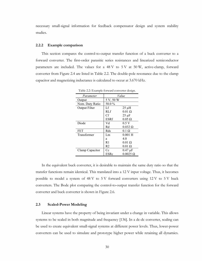
30
necessary small-signal information for feedback compensator design and system stability
studies.
2.2.2 Example comparison
This section compares the control-to-output transfer function of a buck converter to a
forward converter. The first-order parasitic series resistances and linearized semiconductor
parameters are included. The values for a 48 V to 5 V at 50 W, active-clamp, forward
converter from Figure 2.4 are listed in Table 2.2. The double-pole resonance due to the clamp
capacitor and magnetizing inductance is calculated to occur at 3.670 kHz.
Table 2.2: Example forward converter design.
Parameter Value Output 5 V, 50 W Nom. Duty Ratio 50.0 % Output Filter Lf
RLf Cf ESRf
25 µH 0.01 Ω 25 µF 0.05 Ω
Diode Vd Rd
0.5 V 0.032 Ω
FET Rds 0.1 Ω Transformer Lm
a R1 R2
0.001 H 4.0 0.01 Ω 0.01 Ω
Clamp Capacitor Cc ESRc
0.47 µF 0.0025 Ω
In the equivalent buck converter, it is desirable to maintain the same duty ratio so that the
transfer functions remain identical. This translated into a 12 V input voltage. Thus, it becomes
possible to model a system of 48 V to 5 V forward converters using 12 V to 5 V buck
converters. The Bode plot comparing the control-to-output transfer function for the forward
converter and buck converter is shown in Figure 2.6.
2.3 Scaled-Power Modeling
Linear systems have the property of being invariant under a change in variable. This allows
systems to be scaled in both magnitude and frequency [136]. In a dc-dc converter, scaling can
be used to create equivalent small-signal systems at different power levels. Thus, lower-power
converters can be used to simulate and prototype higher power while retaining all dynamics.
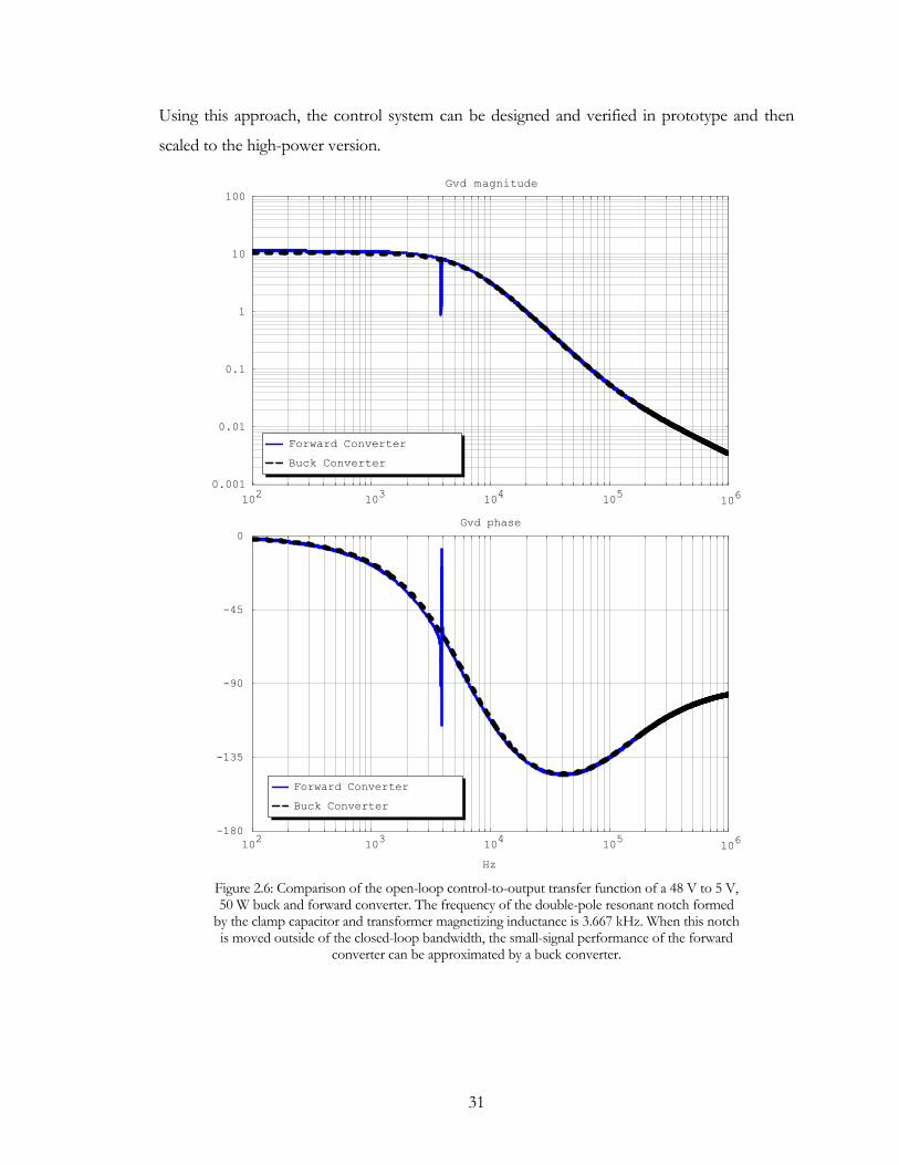
31
Using this approach, the control system can be designed and verified in prototype and then
scaled to the high-power version.
-180
-135
-90
-45
0
Gvd phase
Buck Converter
Forward Converter
0.001
0.01
0.1
1
10
100
Gvd magnitude
Buck Converter
Forward Converter
102
103
104
105
106
102
103
104
105
106
Hz Figure 2.6: Comparison of the open-loop control-to-output transfer function of a 48 V to 5 V, 50 W buck and forward converter. The frequency of the double-pole resonant notch formed
by the clamp capacitor and transformer magnetizing inductance is 3.667 kHz. When this notch is moved outside of the closed-loop bandwidth, the small-signal performance of the forward
converter can be approximated by a buck converter.
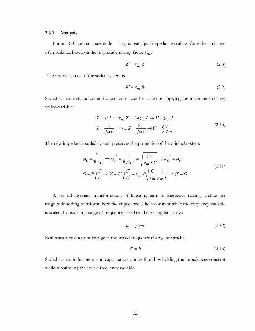
32
2.3.1 Analysis
For an RLC circuit, magnitude scaling is really just impedance scaling. Consider a change
of impedance based on the magnitude scaling factor mγ :
ZZ mγ=′ (2.8)
The real resistance of the scaled system is
RR mγ=′ (2.9)
Scaled-system inductances and capacitances can be found by applying the impedance change
scaled-variable:
m
mm
mmm
CCCj
ZCj
Z
LLLjZLjZ
γωγ
γω
γγωγω
=′→=⇒=
=′→=⇒=
1 (2.10)
The new impedance-scaled system preserves the properties of the original system:
LCR
LCRQ
LCRQ
LCCLLC
mmm
oom
moo
=′→=′′
′=′⇒=
=′→=′′
=′⇒=
γγγ
ωωγγ
ωω
1
11
(2.11)
A second invariant transformation of linear systems is frequency scaling. Unlike the
magnitude scaling transform, here the impedance is held constant while the frequency variable
is scaled. Consider a change of frequency based on the scaling factor fγ :
ωγω f=′ (2.12)
Real resistance does not change in the scaled-frequency change of variables:
RR =′ (2.13)
Scaled-system inductances and capacitances can be found by holding the impedances constant
while substituting the scaled-frequency variable:

33
( )
( ) ff
ff
CCCjCjCj
Z
LLLjLjLjZ
γωγωω
γωγωω
=′→′
=′′
==
=′→′=′′==
111 (2.14)
The new frequency-scaled system scales the frequency terms of the original system but leaves
the damping unchanged:
LCR
LCRQ
LCRQ
CLCLLC
f
f
ofoff
oo
=′→=′′
=′⇒=
=′→=′′
=′⇒=
γ
γ
ωγωγγ
ωω 11
(2.15)
Therefore, in a linear system, a combination of impedance scaling and frequency scaling can be
used to transform a system at one operating point into an invariant system at another
operating point.
In a dc-dc converter, scaling can be used to create equivalent systems at different power
levels. Impedance scaling can be potentially useful to scale the power levels of dc-dc
converters based on the change in load impedance. The advantage to this approach is that
high-power converters can be simulated and prototyped in low-power versions while
preserving the dynamics of the high power system. Using this approach, the control system is
designed and verified in prototype and then simply scaled to the high-power version.
2.3.2 Example: Scaled output filter, constant parasitic resistances
This section compares the control-to-output transfer function of a buck converter
designed for high power to a scaled-power equivalent. The method of impedance scaling is
used where the scaling factor is the ratio of rated power for the full and scaled models. The
parasitic component values are assumed to be the same for both designs. The values for the
48 V to 5 V full-power and scaled-power buck converters are listed in Table 2.3. The ripple
specification was used to determine the output filter values [127].
The result of applying the impedance scaling factor to the filter inductance and capacitance
is shown in Table 2.3. The open-loop control-to-output transfer functions for both designs

34
exhibit second-order characteristics. The cut-off frequency and damping factors are listed in
Table 2.4. The time constants for the filter capacitance are identical for both designs; however,
the filter inductance time constant is slightly shorter for the scaled-power design compared to
the full-power designs. The effect is that the scaled-power design has a slightly higher cut-off
frequency and slightly greater damping.
Table 2.3: Example buck converter: scaled output filter, constant device resistances
Parameter Value Full Power Design Scaled Power Design Input 48 V 48 V Output 5 V, 500 W 5 V, 50 W Switching Frequency 100 kHz 100 kHz Nom. Duty Ratio 12.6% 11.5% Scaling Factor γ 1 0.1 Ripple Specification ∆iL
∆vC ±10% ±2%
Output Filter Lf RLf Cf ESRf
2.7 µH 0.005 Ω 125 µF 0.05 Ω
24.6 µH 0.005 Ω 12.5 µF 0.05 Ω
Diode Vd Rd
0.5 V 0.000 Ω
0.5 V 0.000 Ω
FET Rds 0.010 Ω 0.010 Ω
Table 2.4: Control-to-output transfer function comparison at rated load
Parameter Value Full Power Design Scaled Power Design Rated Load 500 W 50 W Cut-off Frequency 8.638 kHz 9.066 kHz Damping 0.339 0.356
The Bode plots for the two designs are shown in Figure 2.7. The full-power design is
denoted as “HP” and the scaled-power design is denoted as “LP.” For comparison, the
transfer functions are obtained for both designs at both 50 W and 500 W, which represents
10% and 100% of the 500 W rated power for the “HP” design and 100% and 10x of the 50 W
rated power for the “LP” design. The two most relevant curves for direct comparison are the
“HP” and “LP” at respective rated power. The Bode plot reveals good agreement between the
“HP” and “LP” design at lower frequencies but a large discrepancy at higher frequencies,
particularly above the unity-gain frequency. This implies different feedback compensation for
each design if identical closed-loop performance is desired.
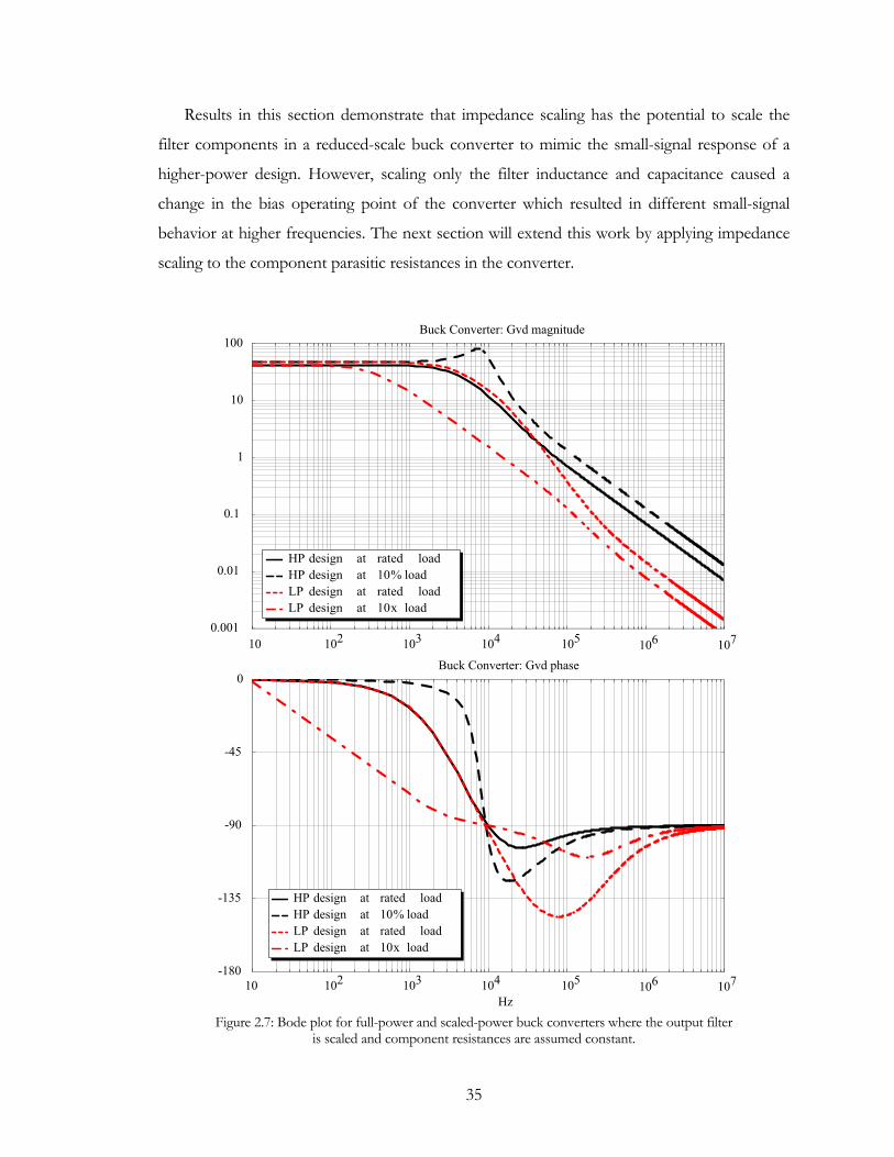
35
Results in this section demonstrate that impedance scaling has the potential to scale the
filter components in a reduced-scale buck converter to mimic the small-signal response of a
higher-power design. However, scaling only the filter inductance and capacitance caused a
change in the bias operating point of the converter which resulted in different small-signal
behavior at higher frequencies. The next section will extend this work by applying impedance
scaling to the component parasitic resistances in the converter.
-180
-135
-90
-45
0Buck Converter: Gvd phase
LP design at 10x load
LP design at rated load
HP design at 10% load
HP design at rated load
0.001
0.01
0.1
1
10
100Buck Converter: Gvd magnitude
LP design at 10x load
LP design at rated load
HP design at 10% load
HP design at rated load
10 102 103 104 105106 107
10 102 103 104 105106 107
Hz Figure 2.7: Bode plot for full-power and scaled-power buck converters where the output filter
is scaled and component resistances are assumed constant.
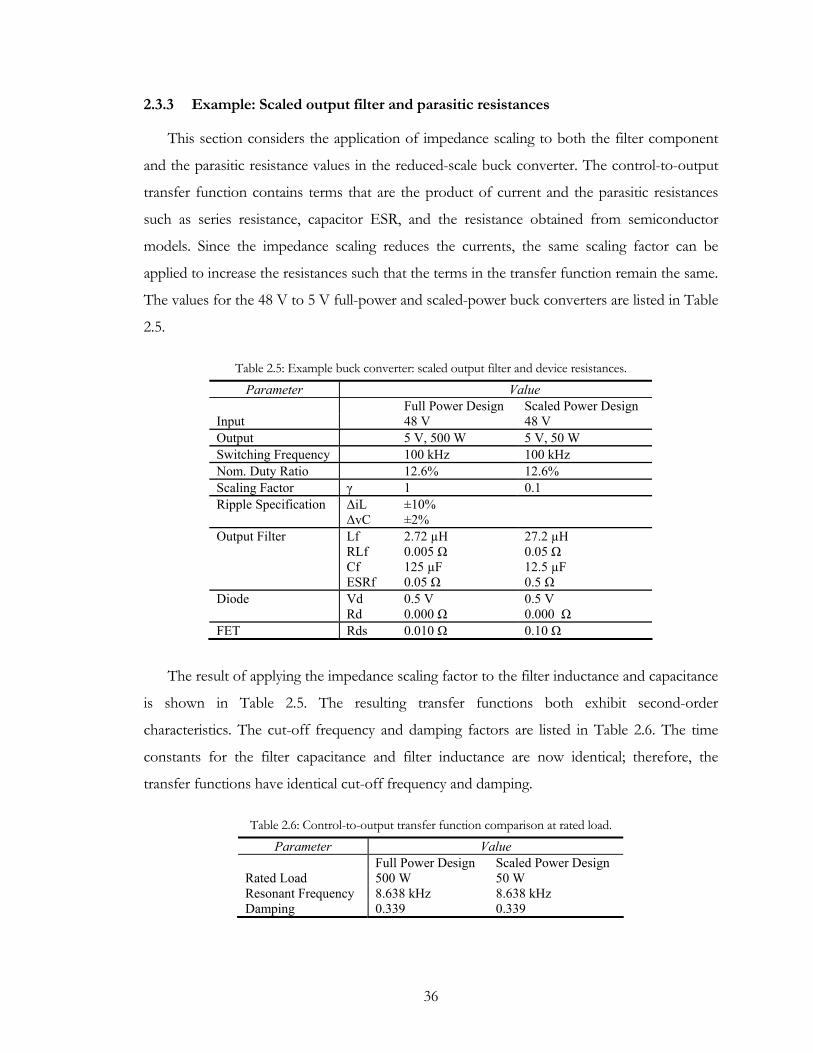
36
2.3.3 Example: Scaled output filter and parasitic resistances
This section considers the application of impedance scaling to both the filter component
and the parasitic resistance values in the reduced-scale buck converter. The control-to-output
transfer function contains terms that are the product of current and the parasitic resistances
such as series resistance, capacitor ESR, and the resistance obtained from semiconductor
models. Since the impedance scaling reduces the currents, the same scaling factor can be
applied to increase the resistances such that the terms in the transfer function remain the same.
The values for the 48 V to 5 V full-power and scaled-power buck converters are listed in Table
2.5.
Table 2.5: Example buck converter: scaled output filter and device resistances.
Parameter Value Full Power Design Scaled Power Design Input 48 V 48 V Output 5 V, 500 W 5 V, 50 W Switching Frequency 100 kHz 100 kHz Nom. Duty Ratio 12.6% 12.6% Scaling Factor γ 1 0.1 Ripple Specification ∆iL
∆vC ±10% ±2%
Output Filter Lf RLf Cf ESRf
2.72 µH 0.005 Ω 125 µF 0.05 Ω
27.2 µH 0.05 Ω 12.5 µF 0.5 Ω
Diode Vd Rd
0.5 V 0.000 Ω
0.5 V 0.000 Ω
FET Rds 0.010 Ω 0.10 Ω
The result of applying the impedance scaling factor to the filter inductance and capacitance
is shown in Table 2.5. The resulting transfer functions both exhibit second-order
characteristics. The cut-off frequency and damping factors are listed in Table 2.6. The time
constants for the filter capacitance and filter inductance are now identical; therefore, the
transfer functions have identical cut-off frequency and damping.
Table 2.6: Control-to-output transfer function comparison at rated load.
Parameter Value Full Power Design Scaled Power Design Rated Load 500 W 50 W Resonant Frequency 8.638 kHz 8.638 kHz Damping 0.339 0.339
37
The Bode plots for the two designs, at their respective rated power, are shown in Figure
2.8. The Bode plot reveals that the two transfer functions are virtually identical. Therefore, the
results in this section demonstrate that impedance scaling can be applied to both the filter
components and other resistive parameters to obtain a reduced-scale buck converter that
mimics the small-signal response of a higher-power design.
180
135
90
45
0Buck Converter: Gvd phase
Scaled power design
Full power design
0.01
0.1
1
10
100Buck Converter: Gvd magnitude
Scaled power design
Full power design
10 102 103 104 105106 107
10 102 103 104 105106 107
Hz Figure 2.8: Bode plot for the full-scale and reduced-scale buck converter where both the output
filter and component resistances are scaled.

38
2.4 Conclusion
Good models capture the salient characteristics of a system such that simulations yield
realistic results and model-based design can be directly applied to the real system. Models in a
power system can benefit from reduction of complexity (reduced order) and reduction of
power level (reduced power). Operational and performance requirements often require the use
of advanced topologies, such as the active-reset forward converter. However, many of these
topologies have fundamental characteristics similar to simpler topologies; that is, the forward
converter has small-signal characteristics similar to a buck converter. This chapter
demonstrated how, with suitable assumptions, the small-signal characteristics of a forward
converter can be approximated with a buck converter. This reduced-order model retains the
important characteristics yet is simpler to model and simulate.
For practical and safety reasons, it is desirable to prototype power systems at reduced-scale
power levels. However, ripple specifications result in different filter designs for different power
levels. In general, as the power level increases, the converter bandwidth decreases as the value
for the filter components increases. This chapter presents one method of applying linear-
system scaling techniques to create reduced-power converters with equivalent small-signal
response. As a design tool, it is beneficial when the dynamics of the full-power system can also
be scaled with the power level so that the resulting control techniques can be directly scaled to
the full-power system.
It is important to recall that the transfer function for a converter is a linearized
representation of the switching power converter at a specific operating point. While it is useful
for the small-signal design and analysis of the converter, it does not uniquely describe the
large-signal operation of the converter nor can it be used to generalize the performance of the
converter at other operating points.
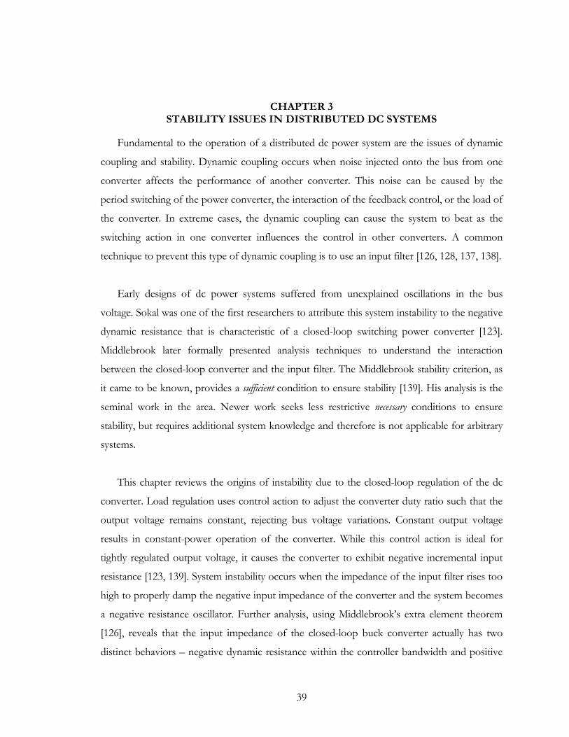
39
CHAPTER 3 STABILITY ISSUES IN DISTRIBUTED DC SYSTEMS
Fundamental to the operation of a distributed dc power system are the issues of dynamic
coupling and stability. Dynamic coupling occurs when noise injected onto the bus from one
converter affects the performance of another converter. This noise can be caused by the
period switching of the power converter, the interaction of the feedback control, or the load of
the converter. In extreme cases, the dynamic coupling can cause the system to beat as the
switching action in one converter influences the control in other converters. A common
technique to prevent this type of dynamic coupling is to use an input filter [126, 128, 137, 138].
Early designs of dc power systems suffered from unexplained oscillations in the bus
voltage. Sokal was one of the first researchers to attribute this system instability to the negative
dynamic resistance that is characteristic of a closed-loop switching power converter [123].
Middlebrook later formally presented analysis techniques to understand the interaction
between the closed-loop converter and the input filter. The Middlebrook stability criterion, as
it came to be known, provides a sufficient condition to ensure stability [139]. His analysis is the
seminal work in the area. Newer work seeks less restrictive necessary conditions to ensure
stability, but requires additional system knowledge and therefore is not applicable for arbitrary
systems.
This chapter reviews the origins of instability due to the closed-loop regulation of the dc
converter. Load regulation uses control action to adjust the converter duty ratio such that the
output voltage remains constant, rejecting bus voltage variations. Constant output voltage
results in constant-power operation of the converter. While this control action is ideal for
tightly regulated output voltage, it causes the converter to exhibit negative incremental input
resistance [123, 139]. System instability occurs when the impedance of the input filter rises too
high to properly damp the negative input impedance of the converter and the system becomes
a negative resistance oscillator. Further analysis, using Middlebrook’s extra element theorem
[126], reveals that the input impedance of the closed-loop buck converter actually has two
distinct behaviors – negative dynamic resistance within the controller bandwidth and positive

40
dynamic resistance outside the controller bandwidth [126]. Each type of behavior places
unique restrictions on the design of an input filter
3.1 Power System Stability
The voltage stability of a power system describes the capability of reaching and sustaining
an acceptable operating point in a controlled way following a disturbance. More formal
definitions can be found in a number of books on the subject [101, 140-142]. Voltage
instability, therefore, is the absence of voltage stability and voltage collapse is the process in
which the power system progresses toward an unacceptable operating point due to voltage
problems.
Weak power systems, such as distributed generation systems and microgrids, are unable to
deliver incremental power and maintain the prescribed system voltage during system
transients. When modeled as a voltage behind impedance, the sources are characterized as
having high impedance which makes the system prone to voltage instability and collapse even
though the steady-state power flow is well below the available maximum power transfer limit.
Constant power loads exacerbate the stability problem by demanding a specific power even if
the system is not capable of delivering it.
3.1.1 Maximum power transfer
Consider the model in Figure 3.1 of a simple power system which comprises a voltage
source sV , a source resistance sR , and a variable resistive load lR . The source resistance in
the model represents the series combination of the equivalent resistance of the source and the
bus impedance. The expression for the power consumed by the load is
lls
sll R
RRVRIP
22
⎟⎟⎠
⎞⎜⎜⎝
⎛+
== (3.1)
Since the relationship between the voltage and the power is quadratic, the voltage at the load is
a solution to the quadratic system:
242
lineloadSSR
RPVVV
−±= (3.2)
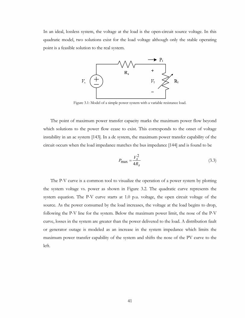
41
In an ideal, lossless system, the voltage at the load is the open-circuit source voltage. In this
quadratic model, two solutions exist for the load voltage although only the stable operating
point is a feasible solution to the real system.
Figure 3.1: Model of a simple power system with a variable resistance load.
The point of maximum power transfer capacity marks the maximum power flow beyond
which solutions to the power flow cease to exist. This corresponds to the onset of voltage
instability in an ac system [143]. In a dc system, the maximum power transfer capability of the
circuit occurs when the load impedance matches the bus impedance [144] and is found to be
s
sR
VP4
2max = (3.3)
The P-V curve is a common tool to visualize the operation of a power system by plotting
the system voltage vs. power as shown in Figure 3.2. The quadratic curve represents the
system equation. The P-V curve starts at 1.0 p.u. voltage, the open circuit voltage of the
source. As the power consumed by the load increases, the voltage at the load begins to drop,
following the P-V line for the system. Below the maximum power limit, the nose of the P-V
curve, losses in the system are greater than the power delivered to the load. A distribution fault
or generator outage is modeled as an increase in the system impedance which limits the
maximum power transfer capability of the system and shifts the nose of the PV curve to the
left.
42
0 0.2 0.4 0.6 0.8 10
0.2
0.4
0.6
0.8
1V
olta
ge [p
u]
Power [pu]
Maxpower
Nominal systemWeakened systemVoltage CollapseResistive load lineConstant power load line
Figure 3.2: P-V curve with resistive load line and constant power load line for a nominal
system, weakened systems, and collapsed system.
Many common loads in a power system have either constant impedance or constant power
characteristics. The load lines for both types are also shown in the P-V curve in Figure 3.2.
The operating point for the system is found graphically as the intersection of the system P-V
curve with the load line. Resistive loads are well-behaved in the sense that as the system
impedance changes, the operating point slides along the load line. Reduced voltage at the load
results in reduced power consumption: an incandescent light bulb dims when the line voltage
drops below the nominal value. Constant-power loads are less system-friendly. As the system
impedance increases (and the voltage drops), the load draws increasing current to maintain
constant power. This results in an operating point at a much lower voltage than with a resistive
load. As the system impedance increases, there is a point where the constant-power load line
and system equation no longer intersect. The system cannot supply the power demanded by
the load and the voltage collapses.
43
3.1.2 Dynamic impedance of loads
While the P-V curve is an excellent tool to understand the steady-state operation of a
power system, it does not capture the dynamic operation of the system. The characteristics of
the load can cause instability that can lead to voltage collapse even if the steady-state power-
flow is stable. This section examines the dynamic impedance for a resistive load and a constant
power load.
When the load in a system is resistive, as shown in Figure 3.1, the constitutive equation for
the terminal characteristic is given by Ohm’s law:
lll RIV = (3.4)
The incremental load impedance is the linearized impedance at the operating point and is
found by differentiating the voltage at the load terminals with respect to the current into the
load:
0~ >=∂∂
= lll
in RIV
R (3.5)
Thus, for a resistive load, the incremental impedance, denoted by the tilde, is positive.
In a closed-loop power converter, regulation uses control action to adjust the converter
duty ratio such that the output voltage remains constant, rejecting variations in both the bus
voltage and load. For a linear resistive load connected to the output of the converter, constant
output converter output voltage requires constant input power for the converter. While the
control action is desirable for good load regulation, it causes the converter to exhibit negative
incremental input resistance [123, 139]. Consider an equivalent circuit to the one shown in
Figure 3.3 where the resistive load is replaced with a dc-dc power supply. The input power of
the converter can be written as
ininin VIP = (3.6)
The incremental input resistance is found by differentiating with respect to current. After
suitable algebraic manipulation, the incremental input resistance is
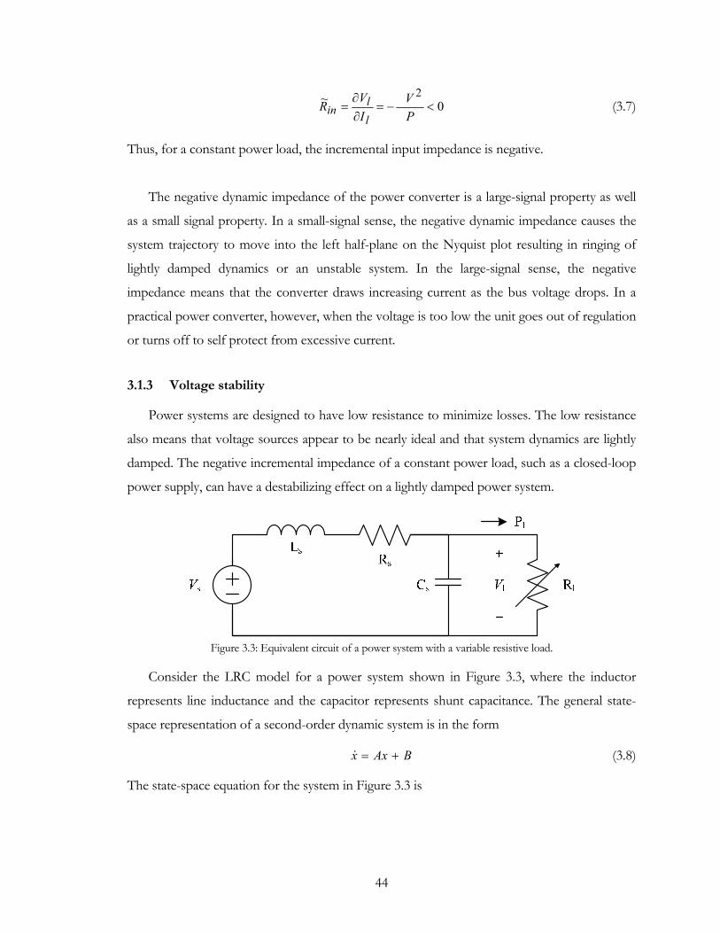
44
0~ 2<−=
∂∂
=PV
IV
Rll
in (3.7)
Thus, for a constant power load, the incremental input impedance is negative.
The negative dynamic impedance of the power converter is a large-signal property as well
as a small signal property. In a small-signal sense, the negative dynamic impedance causes the
system trajectory to move into the left half-plane on the Nyquist plot resulting in ringing of
lightly damped dynamics or an unstable system. In the large-signal sense, the negative
impedance means that the converter draws increasing current as the bus voltage drops. In a
practical power converter, however, when the voltage is too low the unit goes out of regulation
or turns off to self protect from excessive current.
3.1.3 Voltage stability
Power systems are designed to have low resistance to minimize losses. The low resistance
also means that voltage sources appear to be nearly ideal and that system dynamics are lightly
damped. The negative incremental impedance of a constant power load, such as a closed-loop
power supply, can have a destabilizing effect on a lightly damped power system.
Figure 3.3: Equivalent circuit of a power system with a variable resistive load.
Consider the LRC model for a power system shown in Figure 3.3, where the inductor
represents line inductance and the capacitor represents shunt capacitance. The general state-
space representation of a second-order dynamic system is in the form
BAxx +=& (3.8)
The state-space equation for the system in Figure 3.3 is

45
⎥⎥
⎦
⎤
⎢⎢
⎣
⎡+⎥
⎦
⎤⎢⎣
⎡
⎥⎥⎥⎥
⎦
⎤
⎢⎢⎢⎢
⎣
⎡
−
−−=⎥
⎦
⎤⎢⎣
⎡
0L
V
vi
CRC
LLR
vi s
C
L
l
s
C
L11
1
&
& (3.9)
The characteristic polynomial is
( ) [ ]AI −=∆ λλ det (3.10)
The roots of the characteristic polynomial provide the eigenvalues for the system:
012 =+
+⎟⎟⎠
⎞⎜⎜⎝
⎛++
lls
ls
LCRRR
CRLRλλ (3.11)
Stability of the system is assessed by inspection of the eigenvalues. For a stable system,
each coefficient of the characteristic polynomial must be positive. In a trivial case, if the power
system is lossless, 0=sR , then a constant power load with negative incremental impedance
will result in an unstable system. In practice, the power system will have some losses which
provide positive resistance to damp the system dynamics.
3.2 Dynamic Coupling in a DC System
When multiple dc-dc converters are connected in a system, such as in Figure 1.7, the
operation of one point-of-load converter can affect the other converters in the system. An
input filter can help isolate some disturbances from propagating through the system but does
not completely decouple the operation of each point-of-load converter. The degree to which
coupling occurs in the system can be determined by inspection of the system matrix obtained
from the linearized system at the steady-state operating point. The common log of the system
matrix separates the entries by relative order of magnitude.
The system matrix for voltage and current in the three-bus system is given in Table 3.1.
Each point-of-load converter is modeled as a 4 × 4 Jordon block. Two states are from the
output capacitor voltage and inductor current of the buck converter. The second-order input
filter, with suitable damping, contributes two additional states: the filter capacitor voltage and
inductor current. The nonzero off-diagonal terms in the system block represent coupling
between one point-of-load converter (including the input filter) and the other point-of-load

46
converters. In general, a nonlinear system is not uniquely described by a linear system
representation. Therefore, the exact structure of the off-diagonal terms can change depending
on how the states are simplified. The important information obtained here is that the relative
magnitude of the nonzero off-diagonal terms indicates the degree of coupling in the system.
Table 3.1: Linearized system state matrix showing state-coupling.
3 3 2 1 1 3 3 1 1 2 2 1 1 1 1 BUS1.iout
3 3 3 1 1 3 3 1 1 3 3 1 1 2 2 BUS2.iout
2 3 3 1 1 2 2 1 1 3 3 1 1 3 3 BUS3.iout
0 0 0 5 5 0 0 0 0 0 0 0 0 0 0 Buck1.Buck.vc
3 3 0 5 4 5 0 0 0 0 0 0 0 0 0 Buck1.Buck.il
4 4 0 3 3 0 0 0 0 0 0 0 0 0 0 Buck1.input_filter.vc
4 4 3 1 1 3 4 1 1 3 3 1 1 2 1 Buck1.input_filter.il
0 0 0 0 0 0 0 5 5 0 0 0 0 0 0 Buck2.Buck.vc
0 3 3 0 0 0 0 5 4 5 0 0 0 0 0 Buck2.Buck.il
0 4 4 0 0 0 0 3 3 0 0 0 0 0 0 Buck2.input_filter.vc
3 4 4 1 1 3 3 1 1 3 4 1 1 3 3 Buck2.input_filter.il
0 0 0 0 0 0 0 0 0 0 0 5 5 0 0 Buck3.Buck.vc
0 0 3 0 0 0 0 0 0 0 0 5 4 5 0 Buck3.Buck.il
0 0 4 0 0 0 0 0 0 0 0 3 3 0 0 Buck3.input_filter.vc
1 3 4 1 1 2 1 1 1 3 3 1 1 3 4 Buck3.input_filter.il
3.3 Input Filters
Many families of switching dc-dc power converters are characterized by pulsating, non-
continuous, input current. The pulsating current interacts with impedances in the system and
causes voltage perturbations in the distribution bus. The nonideal source impedance of the bus
can also complicate the state-space switching trajectories, increase switch stress, and require
additional circuitry, such as a snubber, to mitigate. One approach to mitigate the deleterious
effects of pulsating input current and provide source impedance matching is the use of an
input filter network [138]. The input filter “smoothes” the input current by providing a shunt
path for the pulsating current – a return path that keeps the pulsating current within the
converter and out of the distribution system. Input filters on power conversion equipment are
often required to ensure compliance with electromagnetic compatibility (EMC) standards
designed to minimize harmful interference [15, 137].

47
A good first choice for an input filter is a capacitor. The ideal filter capacitor has large
energy storage to maintain a constant voltage over the entire switching period and low
impedance at high frequency so that high frequency noise generated by the converter is
shunted away from the distribution bus. However, these two requirements are difficult to
achieve simultaneously with present capacitor technology. In practice, the total input
capacitance might be divided among numerous capacitors: larger electrolytic capacitors to
supply the bulk energy storage and smaller filter grade capacitors to provide the high-frequency
low-impedance shunt. A significant limitation of this solution is that the total capacitance
required is often large, which translates into physically large capacitor bank. At the system
level, large capacitors in the network present current in-rush problems and fault-energy safety
concerns.
A better filter solution is to use a filter network. The simplest network that fulfills the two
filter requirements is the second-order low-pass filter, which is comprised of a series inductor
and a shunt capacitor. The inductor on the input acts as a continuous current source that
provides good source-impedance matching since it is in series with any inductance from the
interconnection and bus. The capacitor on the output provides a nearly ideal voltage source for
the buck converter and a low-impedance shunt path.
Other solutions have been proposed that use interleaved converters to minimize EMI
[145] and active bus conditioners to mitigate system oscillation by providing a local supply of
reactive power near the source of the perturbation [146]. Essentially a fast-switching converter,
the bus conditioner shunts reactive current (ripple current) from the bus by providing extra
energy storage such as a capacitor. Fast switching allows high bandwidth, which helps the
dynamic response of the system. Automatically tuned coupled inductor filters combine passive
filtering with active controls to adjust the filter notch [147-149].
3.4 Middlebrook Stability Criterion
The addition of a passive input filter modifies the dynamics of the system by adding two or
more additional states. In a small-signal sense, the input filter’s output impedance appears in
parallel with the converter’s input impedance. While the dc resistance of the input filter is low
to achieve good efficiency, the impedance of the filter can have more complicated behavior,
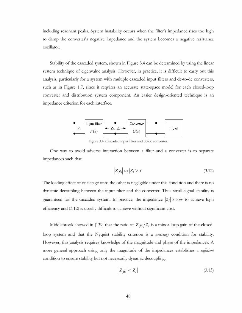
48
including resonant peaks. System instability occurs when the filter’s impedance rises too high
to damp the converter’s negative impedance and the system becomes a negative resistance
oscillator.
Stability of the cascaded system, shown in Figure 3.4 can be determined by using the linear
system technique of eigenvalue analysis. However, in practice, it is difficult to carry out this
analysis, particularly for a system with multiple cascaded input filters and dc-to-dc converters,
such as in Figure 1.7, since it requires an accurate state-space model for each closed-loop
converter and distribution system component. An easier design-oriented technique is an
impedance criterion for each interface.
)(sG)(sF
Figure 3.4: Cascaded input filter and dc-dc converter.
One way to avoid adverse interaction between a filter and a converter is to separate
impedances such that
fZZ ifo ∀<< (3.12)
The loading effect of one stage onto the other is negligible under this condition and there is no
dynamic decoupling between the input filter and the converter. Thus small-signal stability is
guaranteed for the cascaded system. In practice, the impedance iZ is low to achieve high
efficiency and (3.12) is usually difficult to achieve without significant cost.
Middlebrook showed in [139] that the ratio of ifo ZZ is a minor-loop gain of the closed-
loop system and that the Nyquist stability criterion is a necessary condition for stability.
However, this analysis requires knowledge of the magnitude and phase of the impedances. A
more general approach using only the magnitude of the impedances establishes a sufficient
condition to ensure stability but not necessarily dynamic decoupling:
ifo ZZ < (3.13)
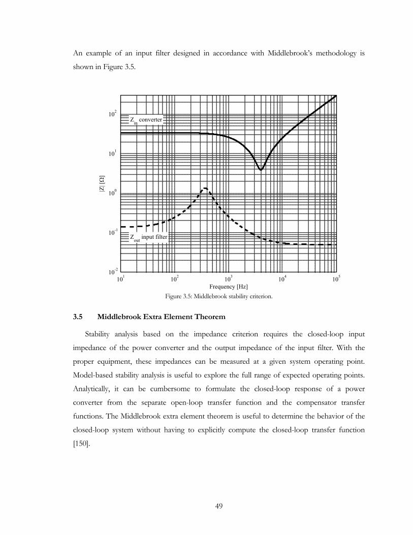
49
An example of an input filter designed in accordance with Middlebrook’s methodology is
shown in Figure 3.5.
101
102
103
104
105
10-2
10-1
100
101
102
Frequency [Hz]
|Z| [Ω
]
Zout
input filter
Zin
converter
Figure 3.5: Middlebrook stability criterion.
3.5 Middlebrook Extra Element Theorem
Stability analysis based on the impedance criterion requires the closed-loop input
impedance of the power converter and the output impedance of the input filter. With the
proper equipment, these impedances can be measured at a given system operating point.
Model-based stability analysis is useful to explore the full range of expected operating points.
Analytically, it can be cumbersome to formulate the closed-loop response of a power
converter from the separate open-loop transfer function and the compensator transfer
functions. The Middlebrook extra element theorem is useful to determine the behavior of the
closed-loop system without having to explicitly compute the closed-loop transfer function
[150].

50
The Middlebrook extra element theorem is used to determine the behavior of a closed-
loop power converter. Two driving point impedances are defined in terms of the converter
input impedance [126]:
( ) ( ) ( ) 0~ →
∆= svinN sZsZ (3.14)
( ) ( ) 0~=
∆= dinD sZsZ (3.15)
where ZN is the input impedance under ideal control action when the output is nulled and ZD is
the open-loop input impedance. The closed-loop buck converter input impedance is a
combination of these driving point impedances with the compensator loop gain:
( ) ( )( )( ) ( ) ( )sTsZsT
sTsZsZ DNin +
++
=1
111
11 (3.16)
Proper control design necessitates large loop-gain at dc to ensure good dc regulation. For
( ) 10 >>T the terms in (3.16) become
( )( ) ( ) 0
11,1
1≈
+≈
+ sTsTsT (3.17)
This results in the input impedance tracking the negative dynamic impedance of the converter
with perfect regulation:
( ) ( )sZsZ Nin
11≈ (3.18)
Above the closed-loop crossover frequency, the loop gain is small: ( ) 10 <T .
( )( ) ( ) 1
11,0
1≈
+≈
+ sTsTsT (3.19)
This results in the input impedance tracking the open-loop converter:
( ) ( )sZsZ Din
11≈ (3.20)
Thus, the Middlebrook extra element theorem shows that the input impedance of the closed-
loop buck converter can be approximated by the negative dynamic resistance of the converter
below the crossover frequency and by the open-loop converter above the crossover frequency.
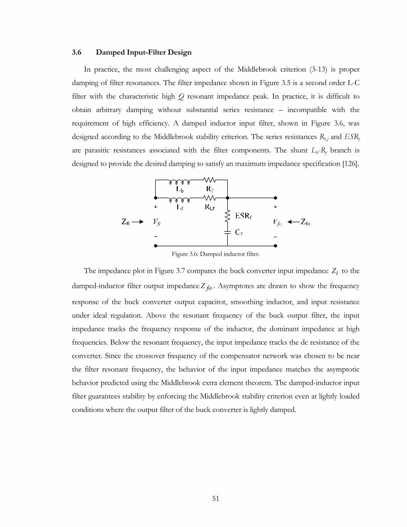
51
3.6 Damped Input-Filter Design
In practice, the most challenging aspect of the Middlebrook criterion (3-13) is proper
damping of filter resonances. The filter impedance shown in Figure 3.5 is a second order L-C
filter with the characteristic high Q resonant impedance peak. In practice, it is difficult to
obtain arbitrary damping without substantial series resistance – incompatible with the
requirement of high efficiency. A damped inductor input filter, shown in Figure 3.6, was
designed according to the Middlebrook stability criterion. The series resistances RLf and ESRf
are parasitic resistances associated with the filter components. The shunt Lb-Rf branch is
designed to provide the desired damping to satisfy an maximum impedance specification [126].
Figure 3.6: Damped inductor filter.
The impedance plot in Figure 3.7 compares the buck converter input impedance iZ to the
damped-inductor filter output impedance foZ . Asymptotes are drawn to show the frequency
response of the buck converter output capacitor, smoothing inductor, and input resistance
under ideal regulation. Above the resonant frequency of the buck output filter, the input
impedance tracks the frequency response of the inductor, the dominant impedance at high
frequencies. Below the resonant frequency, the input impedance tracks the dc resistance of the
converter. Since the crossover frequency of the compensator network was chosen to be near
the filter resonant frequency, the behavior of the input impedance matches the asymptotic
behavior predicted using the Middlebrook extra element theorem. The damped-inductor input
filter guarantees stability by enforcing the Middlebrook stability criterion even at lightly loaded
conditions where the output filter of the buck converter is lightly damped.
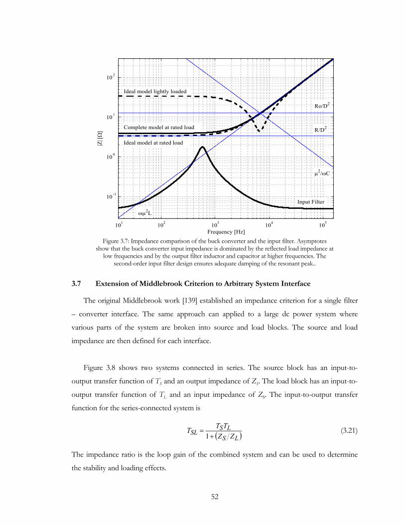
52
102
103
104
105
10-1
100
101
102
Frequency [Hz]
|Z| [Ω
]
ωµ2L
µ2/ωC
R/D2
Ro/D2
Ideal model at rated load
Ideal model lightly loaded
Complete model at rated load
Input Filter
101
Figure 3.7: Impedance comparison of the buck converter and the input filter. Asymptotes
show that the buck converter input impedance is dominated by the reflected load impedance at low frequencies and by the output filter inductor and capacitor at higher frequencies. The
second-order input filter design ensures adequate damping of the resonant peak..
3.7 Extension of Middlebrook Criterion to Arbitrary System Interface
The original Middlebrook work [139] established an impedance criterion for a single filter
– converter interface. The same approach can applied to a large dc power system where
various parts of the system are broken into source and load blocks. The source and load
impedance are then defined for each interface.
Figure 3.8 shows two systems connected in series. The source block has an input-to-
output transfer function of TS and an output impedance of ZS. The load block has an input-to-
output transfer function of TL and an input impedance of ZS. The input-to-output transfer
function for the series-connected system is
( )LSLS
SL ZZTTT
+=
1 (3.21)
The impedance ratio is the loop gain of the combined system and can be used to determine
the stability and loading effects.
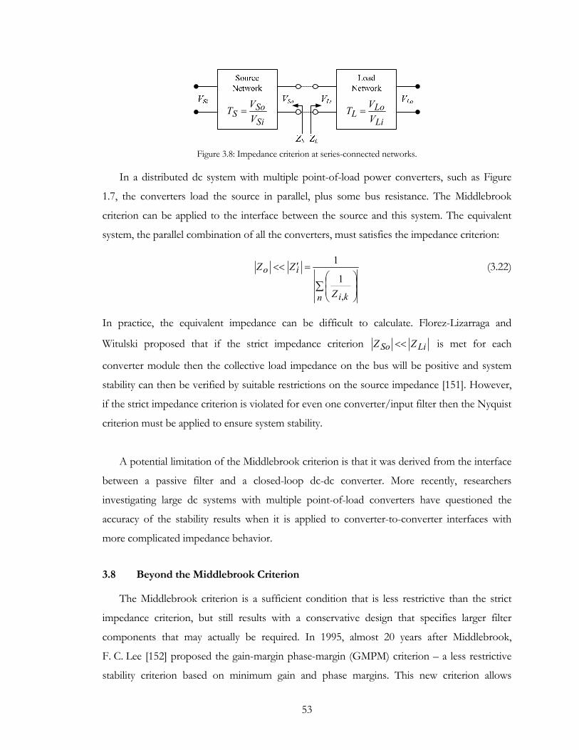
53
SiSo
S VVT =
LiLo
L VVT =
Figure 3.8: Impedance criterion at series-connected networks.
In a distributed dc system with multiple point-of-load power converters, such as Figure
1.7, the converters load the source in parallel, plus some bus resistance. The Middlebrook
criterion can be applied to the interface between the source and this system. The equivalent
system, the parallel combination of all the converters, must satisfies the impedance criterion:
∑ ⎟⎟⎠
⎞⎜⎜⎝
⎛=′<<
n ki
io
Z
ZZ
,
1
1 (3.22)
In practice, the equivalent impedance can be difficult to calculate. Florez-Lizarraga and
Witulski proposed that if the strict impedance criterion LiSo ZZ << is met for each
converter module then the collective load impedance on the bus will be positive and system
stability can then be verified by suitable restrictions on the source impedance [151]. However,
if the strict impedance criterion is violated for even one converter/input filter then the Nyquist
criterion must be applied to ensure system stability.
A potential limitation of the Middlebrook criterion is that it was derived from the interface
between a passive filter and a closed-loop dc-dc converter. More recently, researchers
investigating large dc systems with multiple point-of-load converters have questioned the
accuracy of the stability results when it is applied to converter-to-converter interfaces with
more complicated impedance behavior.
3.8 Beyond the Middlebrook Criterion
The Middlebrook criterion is a sufficient condition that is less restrictive than the strict
impedance criterion, but still results with a conservative design that specifies larger filter
components that may actually be required. In 1995, almost 20 years after Middlebrook,
F. C. Lee [152] proposed the gain-margin phase-margin (GMPM) criterion – a less restrictive
stability criterion based on minimum gain and phase margins. This new criterion allows

54
ifo ZZ > for some frequencies as long as the Nyquist criterion for the loop gain is satisfied for
those frequencies. The loop gain is defined as the ratio of source to load impedance:
LS
m ZZT = (3.23)
In the s-plane, the Middlebrook criterion guarantees stability if the Nyquist plot of the
loop gain stays within the unit circle, as shown in Figure 3.9. However, it says nothing about
the region outside the unit circle. Therefore, a system that lies outside the unit circle may or
may not be stable. The newer GMPM criterion acknowledges that systems with Nyquist plots
that leave the unit circle can be stable, provided they have sufficient gain and phase margin.
The GMPM specifies a “forbidden region” in the s-plane of the loop gain polar plot,
shown in Figure 3.10, that allows the Nyquist diagram to occupy a larger region of the s-plane
than the Middlebrook criterion allows. The forbidden region guarantees minimum phase and
gain margins such that whenever the loop gain crosses the units circle, the phase margin will
always be greater than 60O and that whenever the loop gain crosses to the left of the imaginary
axis, the magnitude of the gain will be less than 0.5 to ensure at least 6 dB gain margin [152].
In a system with multiple load converters, the individual impedance specification for the
kth load converter is derived from the GMPM forbidden region [153]:
source
kload
kLS
PP
ZZ ,
, 21Re ⋅−<⎟
⎟⎠
⎞⎜⎜⎝
⎛ (3.24)
and
( ) kkLSk ZZ Φ++<∠−∠<Φ−− oo 9090 , (3.25)
where
S
kL
S
kLk P
PZ
Z ,,21arcsin ⋅⋅=Φ (3.26)
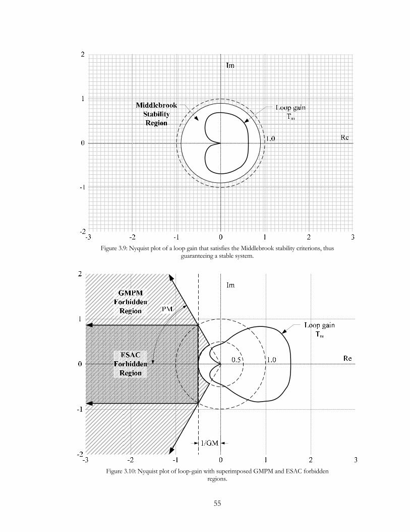
55
Figure 3.9: Nyquist plot of a loop gain that satisfies the Middlebrook stability criterions, thus
guaranteeing a stable system.
Figure 3.10: Nyquist plot of loop-gain with superimposed GMPM and ESAC forbidden
regions.

56
The GMPM criterion relaxes the conservative requirements of the Middlebrook criterion,
but requires that phase and magnitude information for both the source and load be measured
and the loop gain calculated. Therefore it is more appropriate for a closed, fixed-topology
system where all parameters are known a priori. Subsequent work has sought to reduce the
area of the forbidden region while at the same time accounting for some parameters’
uncertainty. The ESAC stability criterion, also shown in Figure 3.10, is based on the principles
of the GMPM but allows greater design flexibility by reducing the forbidden region [40].
3.9 Conclusions
Stability is an important concept in a dc system that has received significant attention since
Sokal published the first link between closed-loop dc-dc converters and system instability in
1973. Since then, researchers have sought design and analysis tools to specify and verify stable
system operation. A conservative criterion, like the Middlebrook criterion, provides sufficient
conditions to ensure robust system stability but often results in an expensive solution. More
recent work has sought a less conservative criterion that allows violation of the Middlebrook
criterion but requires more detailed knowledge of the entire system. A survey of the literature
reveals that these newer techniques were developed for specific applications and system
topologies. An open area for future research is to develop a unified stability criterion that can
be applied to arbitrary dc systems.
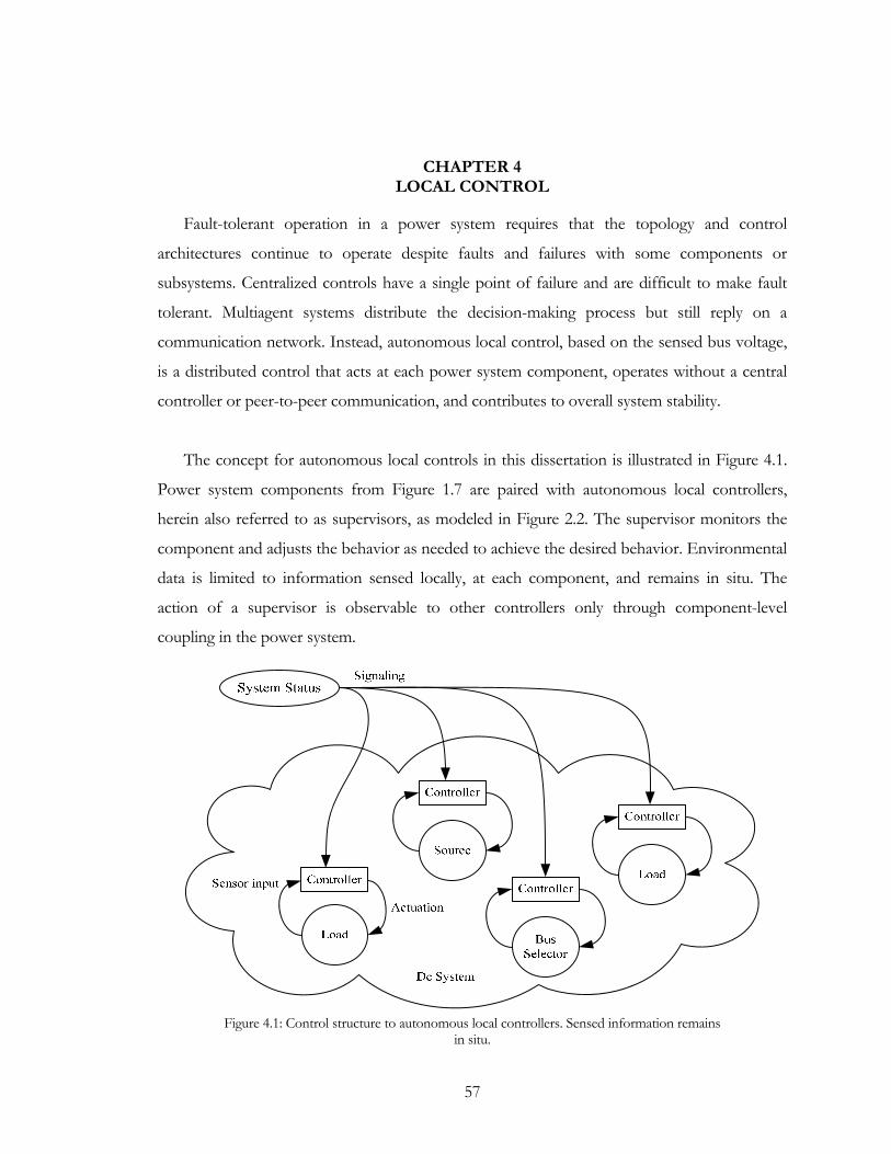
57
CHAPTER 4 LOCAL CONTROL
Fault-tolerant operation in a power system requires that the topology and control
architectures continue to operate despite faults and failures with some components or
subsystems. Centralized controls have a single point of failure and are difficult to make fault
tolerant. Multiagent systems distribute the decision-making process but still reply on a
communication network. Instead, autonomous local control, based on the sensed bus voltage,
is a distributed control that acts at each power system component, operates without a central
controller or peer-to-peer communication, and contributes to overall system stability.
The concept for autonomous local controls in this dissertation is illustrated in Figure 4.1.
Power system components from Figure 1.7 are paired with autonomous local controllers,
herein also referred to as supervisors, as modeled in Figure 2.2. The supervisor monitors the
component and adjusts the behavior as needed to achieve the desired behavior. Environmental
data is limited to information sensed locally, at each component, and remains in situ. The
action of a supervisor is observable to other controllers only through component-level
coupling in the power system.
Figure 4.1: Control structure to autonomous local controllers. Sensed information remains
in situ.

58
Droop control is used for the power sources, which means that the system voltage is not
fixed. Changes in the bus voltage carry useful information about the system such as partial loss
of generation, increase in system damping, or increased loading. Supervisor controls at the load
sense that the bus voltage has changed but are unaware of how or why. If the sensed bus
voltage drops too low or too quickly, the supervisor can direct the component to take action
that abates further voltage decline. On the load-side, these actions include bus selection, power
buffering, or load interruption.
A dc system facilitates control of individual loads for performance and coordination,
especially as energy allocation priorities change to match operational priorities. Load priority is
critical because it provides a structure approach to the control process. If the bus voltage
drops, signaling a problem in the system, mission-critical loads can remain active while less
important loads automatically revert to a “safe” mode. Situation awareness, provided by low
bandwidth signaling allows the supervisor to adjust the priority of its load and fine tune the
component operation. However, the local control continues to sense information from the bus
and can functions autonomously in the absence of the system-level data.
This chapter presents a technique to integrate the load-side controls of the power buffer,
bus selector, and dynamic load interrupter to support system operation through all types of
system and load events, prevent voltage collapse, and support automatic recovery upon system
stabilization.
4.1 Load-Control Strategies for System Stability
It is well known that the interconnection of a large number of high-bandwidth nonlinear
dc power converters creates potential stability problems. Tight output voltage regulation
enforces constant power behavior and negative dynamic input impedance, which was shown
in Chapter 3 to have a destabilizing effect on the system, particularly during voltage sag. In a
large-signal sense, the bus voltage in a dc system can sag for a number of reasons including
loss of generation or increase in load. Finite inertia dc systems, such as shipboard power, are
characteristically weak. Without spinning reserves or other stability mechanisms present in the
ac terrestrial grid, such systems are subject to extreme voltage sags or even voltage collapse.
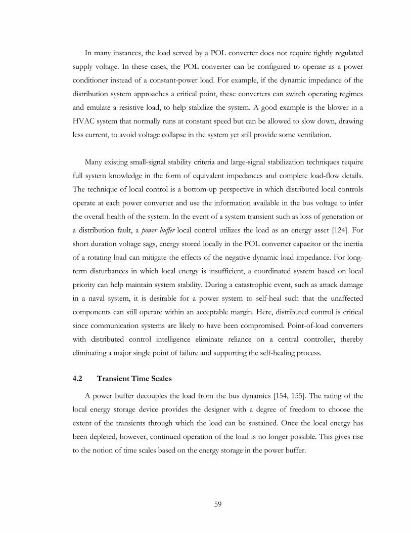
59
In many instances, the load served by a POL converter does not require tightly regulated
supply voltage. In these cases, the POL converter can be configured to operate as a power
conditioner instead of a constant-power load. For example, if the dynamic impedance of the
distribution system approaches a critical point, these converters can switch operating regimes
and emulate a resistive load, to help stabilize the system. A good example is the blower in a
HVAC system that normally runs at constant speed but can be allowed to slow down, drawing
less current, to avoid voltage collapse in the system yet still provide some ventilation.
Many existing small-signal stability criteria and large-signal stabilization techniques require
full system knowledge in the form of equivalent impedances and complete load-flow details.
The technique of local control is a bottom-up perspective in which distributed local controls
operate at each power converter and use the information available in the bus voltage to infer
the overall health of the system. In the event of a system transient such as loss of generation or
a distribution fault, a power buffer local control utilizes the load as an energy asset [124]. For
short duration voltage sags, energy stored locally in the POL converter capacitor or the inertia
of a rotating load can mitigate the effects of the negative dynamic load impedance. For long-
term disturbances in which local energy is insufficient, a coordinated system based on local
priority can help maintain system stability. During a catastrophic event, such as attack damage
in a naval system, it is desirable for a power system to self-heal such that the unaffected
components can still operate within an acceptable margin. Here, distributed control is critical
since communication systems are likely to have been compromised. Point-of-load converters
with distributed control intelligence eliminate reliance on a central controller, thereby
eliminating a major single point of failure and supporting the self-healing process.
4.2 Transient Time Scales
A power buffer decouples the load from the bus dynamics [154, 155]. The rating of the
local energy storage device provides the designer with a degree of freedom to choose the
extent of the transients through which the load can be sustained. Once the local energy has
been depleted, however, continued operation of the load is no longer possible. This gives rise
to the notion of time scales based on the energy storage in the power buffer.
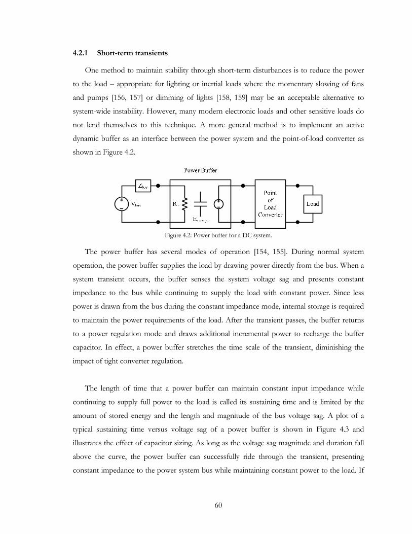
60
4.2.1 Short-term transients
One method to maintain stability through short-term disturbances is to reduce the power
to the load – appropriate for lighting or inertial loads where the momentary slowing of fans
and pumps [156, 157] or dimming of lights [158, 159] may be an acceptable alternative to
system-wide instability. However, many modern electronic loads and other sensitive loads do
not lend themselves to this technique. A more general method is to implement an active
dynamic buffer as an interface between the power system and the point-of-load converter as
shown in Figure 4.2.
Figure 4.2: Power buffer for a DC system.
The power buffer has several modes of operation [154, 155]. During normal system
operation, the power buffer supplies the load by drawing power directly from the bus. When a
system transient occurs, the buffer senses the system voltage sag and presents constant
impedance to the bus while continuing to supply the load with constant power. Since less
power is drawn from the bus during the constant impedance mode, internal storage is required
to maintain the power requirements of the load. After the transient passes, the buffer returns
to a power regulation mode and draws additional incremental power to recharge the buffer
capacitor. In effect, a power buffer stretches the time scale of the transient, diminishing the
impact of tight converter regulation.
The length of time that a power buffer can maintain constant input impedance while
continuing to supply full power to the load is called its sustaining time and is limited by the
amount of stored energy and the length and magnitude of the bus voltage sag. A plot of a
typical sustaining time versus voltage sag of a power buffer is shown in Figure 4.3 and
illustrates the effect of capacitor sizing. As long as the voltage sag magnitude and duration fall
above the curve, the power buffer can successfully ride through the transient, presenting
constant impedance to the power system bus while maintaining constant power to the load. If
61
the transient event begins to approach the sustaining time limit, then the local load control
needs to switch strategies to maintain stability.
10-2 10-1 100 101 1020
0.2
0.4
0.6
0.8
1
Time (s)
Bus
Vol
tage
[P.U
.]
Ride through cap ability
Insufficient energy storage
220uF470uF1000uF
Figure 4.3: Sustaining time capability [124].
4.2.2 Long-term transients
System transients that exceed the sustaining time of the power buffer (or that are caused
by topological failures such as loss of generation or a bus fault) require an alternative technique
to mitigate system instability and voltage collapse. In this case, the only long-term strategy to
stabilize an energy-constrained dc system is to switch to another supply or to load shed [9,
111].
In practice, dc-dc regulators have minimum allowable input voltages that prevent them
from operating as true constant power loads. As the system bus voltage decreases due to
increased loading or loss of generation, these converters will turn off to self protect as the bus
voltage decreases below this specified voltage limit. In a radial system, the voltage drop along
the bus due to bus impedance automatically gives rise to a notion of priority to the loads located
closest to the source and hence with the highest bus voltage. Thus, the first converters shed in
due to UVP are the ones physically farthest from the source. This behavior directly couples the
system topology to the load priority. In general, it is not desirable that the topology dictate
priority. Instead, a supervisor control at each POL converter monitors the bus voltage and
turns off the converter based on the priority of the load. Mapping the priority setting to a

62
particular bus voltage forces loads with the lowest priority to be shed first and allows higher
priority loads to remain energized, regardless of location in the system. Thus system operation
is decoupled from system topology. A similar technique has been proposed for ring-bus
architectures [10].
4.3 Load Prioritization and Scheduling
In an energy-constrained system, load prioritization is critical for system stability and
control because it provides a structured approach to the decision and control process. It is
likely that a particular load’s priority may need to change depending on the operation of the
system. In a naval ship, each load is classified as either nonessential, semiessential, or essential
[9]. A general framework for organizing the load priorities is a two-dimensional matrix as
shown in Table 4.1. In one example, propulsion is considered the highest priority while hotel
loads such as lighting in crew quarters and power in the galley are less important and can be
sacrificed depending on the threat level. In another example, the launch equipment for
lifeboats has a higher priority under “Patrol” status for safety reasons but yields priority to
other systems such as weapons and propulsion under “General Quarters” status. If local
energy is available in a power buffer, load priority is useful to determine if the load simply
turns off or the power buffer operates when trouble is sensed on the dc bus. If a redundant
distribution system is provided, such as the dual bus system in Figure 1.1, load priority can be
used to determine if the load seeks alternative power sources when the primary system begins
to fail.
Table 4.1: Load priority-assignment example.
Fine-tuning the performance of the system requires that each POL converter has some
information about the entire system. Low-bandwidth signaling from the command and control
center can broadcast the current state of the system, but each POL converter ultimately

63
decides how to use the information – unlike in a centralized control scheme where each load is
directly controlled. The distributed control strategy is inherently fault-tolerant because each
controller acts independently. If the low-bandwidth communication is compromised, each
controller can continue to operate using the last-known state, or revert to fail-safe operation as
determined by the load-priority table.
4.4 Nature of the Disturbance
System changes due to load, generation, or topological change are observed in the bus
voltage. These changes can occur at different rates of time and are conveniently divided into
three categories: step, low-frequency, and high-frequency. The nature of the transient event
and the priority of the load determine the best controller response. Step events occur when the
dc bus voltage suddenly changes, such as when loads are added or removed or the power
drawn by a load changes precipitously. The new system is assumed to be sufficiently damped
with a stable operating point. Low-frequency events include system-wide oscillations and
slowly changing voltage profiles. Low-frequency bus oscillations may be the result of excitation
of a resonant frequency, an underdamped response, or chattering as multiple converters
interact. High-frequency events are characterized by a high dv/dt bus voltage. Additionally, the
frequency and total number of transient events can provide valuable knowledge of the system’s
health.
4.5 Integrated Local-Control Strategy
Control strategy for each POL bus interface depends on the load priority. High priority
loads are required to continue operation while lower priority loads can be turned off to
preserve the voltage stability of the system. A power buffer on the higher priority loads eases
the burden on the bus by presenting constant input impedance instead of a constant power
load during a buffering event. In this mode, current is still drawn from the bus and internal
energy storage satisfies the load requirements. A bus selector can seek alternate sources of
energy. Dynamic load interruption turns off loads in priority order when there is no other
choice.
Figure 4.4 illustrates the decision logic for a complete POL power unit.
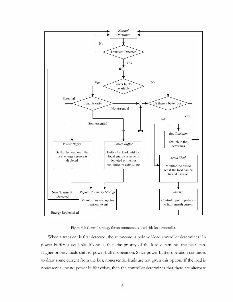
64
Load Priority
Load Shed
Monitor the bus to see if the load can be
turned back on
Nonessential
Semiessential
Essential
New Transient Detected
Yes
Startup
Control input impedance to limit inrush current
Power Buffer
Buffer the load until the local energy reserve is
depleted or the bus continues to deteriorate
Power Buffer
Buffer the load until the local energy reserve is
depleted
Replenish Energy Storage
Monitor bus voltage for transient event
Energy Replenished
Transient Detected
Power bufferavailable
No
Bus Selection
Switch to the better bus
Normal Operation
Is there a better bus
Yes
No
Yes
No
Figure 4.4: Control strategy for an autonomous, load-side load controller.
When a transient is first detected, the autonomous point-of-load controller determines if a
power buffer is available. If one is, then the priority of the load determines the next step.
Higher priority loads shift to power buffer operation. Since power buffer operation continues
to draw some current from the bus, nonessential loads are not given this option. If the load is
nonessential, or no power buffer exists, then the controller determines that there are alternate

65
supply buses. If an alternate bus is available, then bus selection changes the supply bus. If there
are no others then the nonessential load must be shed.
In power buffer operation, for essential loads, the wellbeing of the load is favored;
therefore, the buffer will attempt to maintain the load until its internal energy storage is
depleted, while presenting constant input impedance to the bus. When the internal energy has
been depleted, but the bus has not yet recovered, the POL switches to load-shed strategy. For
a semiessential load, the loads welfare is favored less. Throughout a protection event, the input
impedance remains constant, while stored energy supplements the load power. However, if
during the protection event, the bus condition becomes worse, the strategy is switched to a
load shed.
If the bus recovers from a transient, the power buffer changes to replenish energy storage
mode. While drawing full load power from the bus to supply the needs of the load, additional
power is drawn to recharge the buffer energy storage capacitor. If during the replenish cycle
the bus experiences another transient, then the buffer re-enters a constant input impedance
mode. Since the replenish cycle was interrupted, the sustaining time for the latest transient will
be diminished as there is less stored energy. If the replenish cycle finishes uninterrupted by a
bus transient, then the buffer returns to normal operation.
If a load was shed, when the initiating event clears and the system stabilizes, a startup
strategy is implemented. To minimize the chance of triggering further system transients, the
bus power to the load should be minimized during startup. Figure 4.5 presents a control
flowchart for the priority-based startup sequence. When the load is essential, power is
immediately delivered to the load. When a semiessential or nonessential load is started, the
power buffer is used to soft-start, eliminating inrush current and gracefully loading the bus
with an initial constant impedance to help stabilize the system. After a time, the power buffer
will revert to normal operation. If a bus transient occurs during precharging of the buffer, then
the charging cycle ends for lower priority loads until the bus returns to its nominal state.
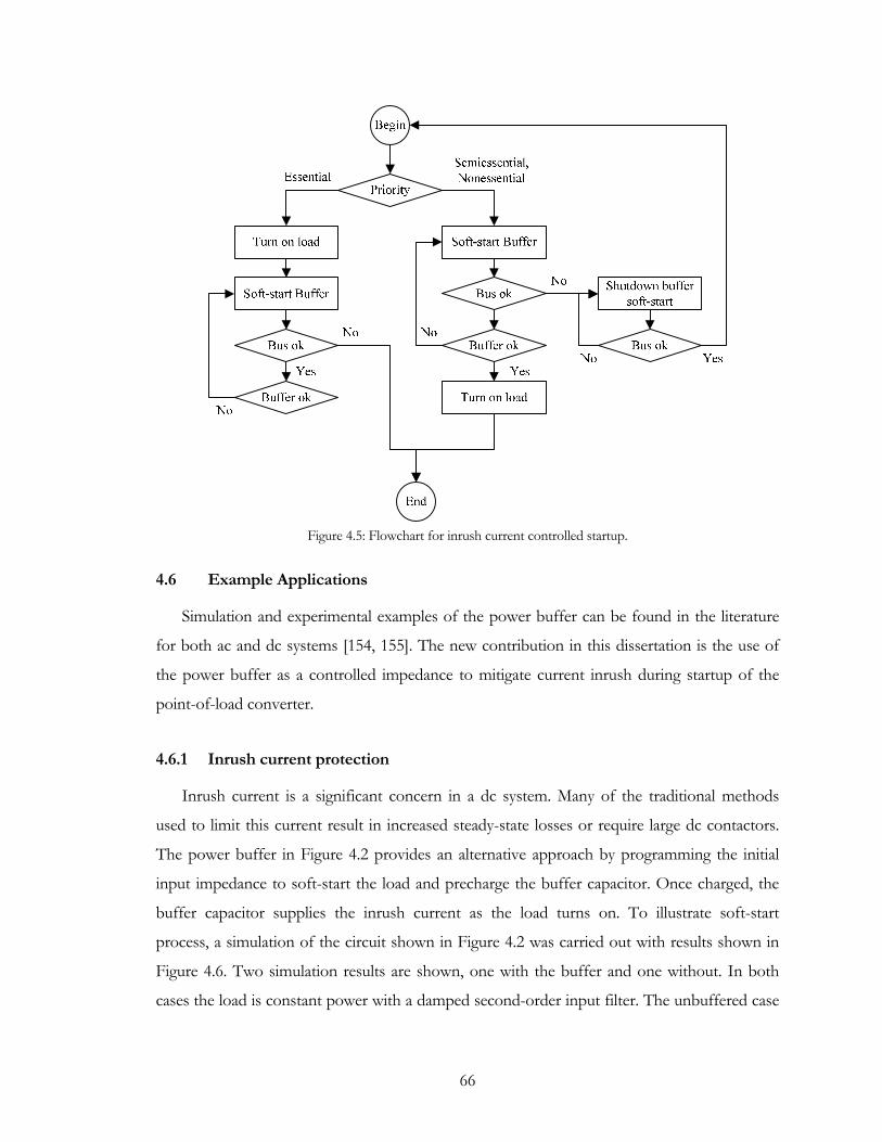
66
Figure 4.5: Flowchart for inrush current controlled startup.
4.6 Example Applications
Simulation and experimental examples of the power buffer can be found in the literature
for both ac and dc systems [154, 155]. The new contribution in this dissertation is the use of
the power buffer as a controlled impedance to mitigate current inrush during startup of the
point-of-load converter.
4.6.1 Inrush current protection
Inrush current is a significant concern in a dc system. Many of the traditional methods
used to limit this current result in increased steady-state losses or require large dc contactors.
The power buffer in Figure 4.2 provides an alternative approach by programming the initial
input impedance to soft-start the load and precharge the buffer capacitor. Once charged, the
buffer capacitor supplies the inrush current as the load turns on. To illustrate soft-start
process, a simulation of the circuit shown in Figure 4.2 was carried out with results shown in
Figure 4.6. Two simulation results are shown, one with the buffer and one without. In both
cases the load is constant power with a damped second-order input filter. The unbuffered case
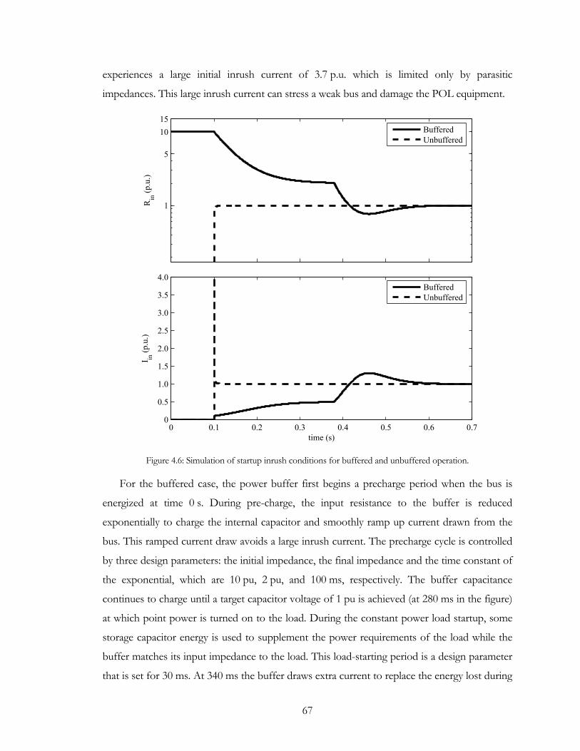
67
experiences a large initial inrush current of 3.7 p.u. which is limited only by parasitic
impedances. This large inrush current can stress a weak bus and damage the POL equipment.
1
5
1015
Rin
(p.u
.)
BufferedUnbuffered
0 0.1 0.2 0.3 0.4 0.5 0.6 0.70
0.5
1.0
1.5
2.0
2.5
3.0
3.5
4.0
time (s)
I in (p
.u.)
BufferedUnbuffered
Figure 4.6: Simulation of startup inrush conditions for buffered and unbuffered operation.
For the buffered case, the power buffer first begins a precharge period when the bus is
energized at time 0 s. During pre-charge, the input resistance to the buffer is reduced
exponentially to charge the internal capacitor and smoothly ramp up current drawn from the
bus. This ramped current draw avoids a large inrush current. The precharge cycle is controlled
by three design parameters: the initial impedance, the final impedance and the time constant of
the exponential, which are 10 pu, 2 pu, and 100 ms, respectively. The buffer capacitance
continues to charge until a target capacitor voltage of 1 pu is achieved (at 280 ms in the figure)
at which point power is turned on to the load. During the constant power load startup, some
storage capacitor energy is used to supplement the power requirements of the load while the
buffer matches its input impedance to the load. This load-starting period is a design parameter
that is set for 30 ms. At 340 ms the buffer draws extra current to replace the energy lost during
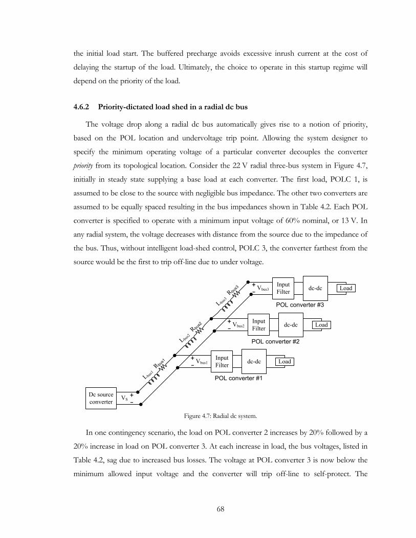
68
the initial load start. The buffered precharge avoids excessive inrush current at the cost of
delaying the startup of the load. Ultimately, the choice to operate in this startup regime will
depend on the priority of the load.
4.6.2 Priority-dictated load shed in a radial dc bus
The voltage drop along a radial dc bus automatically gives rise to a notion of priority,
based on the POL location and undervoltage trip point. Allowing the system designer to
specify the minimum operating voltage of a particular converter decouples the converter
priority from its topological location. Consider the 22 V radial three-bus system in Figure 4.7,
initially in steady state supplying a base load at each converter. The first load, POLC 1, is
assumed to be close to the source with negligible bus impedance. The other two converters are
assumed to be equally spaced resulting in the bus impedances shown in Table 4.2. Each POL
converter is specified to operate with a minimum input voltage of 60% nominal, or 13 V. In
any radial system, the voltage decreases with distance from the source due to the impedance of
the bus. Thus, without intelligent load-shed control, POLC 3, the converter farthest from the
source would be the first to trip off-line due to under voltage.
R bus3
L bus3
R bus2
L bus2
POL converter #3
POL converter #2
InputFilter dc-dc
POL converter #1
R bus1
L bus1
Dc source converter
+ -
Vbus2
+ -
Vbus3
+ -
Vbus1InputFilter dc-dc
InputFilter dc-dc
+ -
VS
Load
Load
Load
Figure 4.7: Radial dc system.
In one contingency scenario, the load on POL converter 2 increases by 20% followed by a
20% increase in load on POL converter 3. At each increase in load, the bus voltages, listed in
Table 4.2, sag due to increased bus losses. The voltage at POL converter 3 is now below the
minimum allowed input voltage and the converter will trip off-line to self-protect. The
69
dynamic load-shed controller allows each converter’s set-points to be chosen such that the
load is shed according to its priority listed in Table 4.2.
Table 4.2: Operational parameters for the radial system POLC 1 POLC 2 POLC 3
Priority Essential Nonessential Essential Vin after contingency without load shed control
21.404 V 14.191 V 10.020 V
Vin after contingency with load shed control
21.714 V 19.087 V 16.479 V
Vmin set point 13.000 V 15.850 V 13.000 V Vmax set point 13.000 V 19.550 V 13.000 V Rbus 0.01 Ω 1.00 Ω 1.00 Ω Pload (base) 30 W 30 W 30 W
4.7 Conclusions
Reliability in a dc power system is enhanced though a control architecture that is fault
tolerant. This means that a fault or failure at one or more components or controls does not
prevent the remaining system from working according to design. This chapter presented a
concept where controls at each component operate autonomously, obtain system information
by sensing the bus voltage, and do not rely on communication to perform their function.
Variable system voltage conveys information about the health of the system. The controls
sense and react to the changing bus voltage without needing to know why or how it changed.
Prioritization provides a structured approach to load control when a system event occurs. A
load-side control strategy was presented that integrates a power buffer, bus selection, and load
interruption with load priority. Lastly, examples of using load priority to decouple the load
operation from the topology and using a power buffer to control inrush current on startup
were presented.
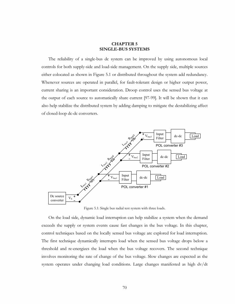
70
CHAPTER 5 SINGLE-BUS SYSTEMS
The reliability of a single-bus dc system can be improved by using autonomous local
controls for both supply-side and load-side management. On the supply side, multiple sources
either colocated as shown in Figure 5.1 or distributed throughout the system add redundancy.
Whenever sources are operated in parallel, for fault-tolerant design or higher output power,
current sharing is an important consideration. Droop control uses the sensed bus voltage at
the output of each source to automatically share current [97-99]. It will be shown that it can
also help stabilize the distributed system by adding damping to mitigate the destabilizing affect
of closed-loop dc-dc converters.
bu
s3
bus3
bus2
bus2
POL converter #3
POL converter #2
InputFilter dc-dc
POL converter #1
bus1
bus1
Dc source converter
+ -
Vbus2
+ -
Vbus3
+ -
Vbus1InputFilter dc-dc
InputFilter dc-dc
+ -
VS
Load
Load
Load
Figure 5.1: Single bus radial test system with three loads.
On the load side, dynamic load interruption can help stabilize a system when the demand
exceeds the supply or system events cause fast changes in the bus voltage. In this chapter,
control techniques based on the locally sensed bus voltage are explored for load interruption.
The first technique dynamically interrupts load when the sensed bus voltage drops below a
threshold and re-energizes the load when the bus voltage recovers. The second technique
involves monitoring the rate of change of the bus voltage. Slow changes are expected as the
system operates under changing load conditions. Large changes manifested as high dv/dt

71
suggest undesirable or unstable changes in the system and will be used to initiate dynamic load
interruption.
Load restoration is a more difficult automatic control problem than load interruption. The
objective of restoration is to maximize the number of loads supplied without causing system
instability [110]. Heuristic techniques that restore power to one load at a time and stop to
check system operation between steps are slow and require either a central controller or multi-
agent approach. Autonomous local controls monitor the bus and restore load operation when
the bus voltage reaches the turn-on threshold.
In this work, the values of the threshold voltage for load interruption were initially
determined by an exhaustive power flow contingency analysis followed by a search algorithm.
Since this formulation is specific to the system in Figure 5.1, the problem is generalized and
cast into a bilevel integer programming framework suitable for an arbitrary system. However,
the bilevel program still requires data from a contingency analysis. While this analysis is likely
to be performed for large systems such as the future naval shipboard power system [110, 160],
it may not be for smaller dc systems. System reliability is improved if the voltage thresholds are
determined on-line by each autonomous local controller. It will be shown that load
interruption affects the impedance ratio at the interface between the bus and the point-of-load
converter. This suggests that the loop gain in (3.23) could be mapped to a voltage threshold in
future work.
Extensive custom hardware was designed and built to experimentally verify load-side
control. The hardware includes a point-of-load buck dc-to-dc converter, a microcontroller outer-
loop supervisor for each POL converter, and forced-convection cooled resistive loads for the
converters and simulated bus impedances. The buck converter has an analog voltage-mode
controller built from discrete components to allow full control over the PWM process. The
outer-loop controller that performs the autonomous local control is implemented digitally in a
PIC® microcontroller. Design and operational details for both the buck converter and the PIC
system are provided in Appendix A.
72
5.1 Supply-Side: Droop Control
In a dc system where multiple source converters supply the same bus, current sharing is an
important consideration. Theoretically, identical supply converters will share the load current
equally. However, mismatches in components and feedback networks as well as different
impedances at different locations on the bus can cause imbalance in current sharing. If
significant, this imbalance can result in overload and thermal stresses which could jeopardize
system reliability. The methods for load sharing reported in the literature fall into two groups:
active sharing and droop control [97, 100]. Droop control is the focus in this work because it is
a form of autonomous local control.
Active current-sharing techniques involve a control structure and a method of
programming individual converters with a reference current. One implementation is to use a
master/slave configuration such that one dc source is designated as the master and is used to
control the bus voltage. The remaining dc sources, designated as slaves, operate as current
sources. This strategy produces a stiff bus voltage and controlled load dispatch at each source.
There are two main limitations of this technique: high-speed communication is required and a
single point failure can disable the entire system [161]. In practice, active current sharing
techniques are best suited for physically small systems, such as paralleled voltage regulator
module (VRM) applications. If the topology were fixed and known a priori, more sophisticated
controls such as interleaving can be used to reduce ripple [162].
In droop control, the output voltage of the source drops as current increases. This is a
form of local control since converters autonomously share load current by sensing the local
bus voltage. Droop control can be as simple as a series resistance or a more efficient closed-
loop controller such as a phase-angle controller in a rectifier source converter. This scheme has
been proposed for use in large-scale distributed systems [99] with dynamically changing
topologies since it supports plug-and-play reconfiguration and system scaling, and is robust to
component failures.
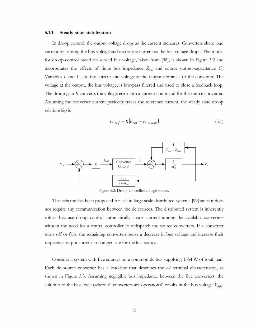
73
5.1.1 Steady-state stabilization
In droop control, the output voltage drops as the current increases. Converters share load
current by sensing the bus voltage and increasing current as the bus voltage drops. The model
for droop-control based on sensed bus voltage, taken from [98], is shown in Figure 5.2 and
incorporates the effects of finite bus impedance Zbus and source output-capacitance Cs.
Variables Is and Vs are the current and voltage at the output terminals of the converter. The
voltage at the output, the bus voltage, is low-pass filtered and used to close a feedback loop.
The droop gain K converts the voltage error into a current command for the source converter.
Assuming the converter current perfectly tracks the reference current, the steady state droop
relationship is
( )sensesrefrefs vVKI ,, −= (5.1)
K Converter Gconv(s) SsC
1
loadbus ZZ +1
Vref
LP
LP
s ωω+
Vs
Is,ref Is
+-+-
Figure 5.2: Droop-controlled voltage source.
This scheme has been proposed for use in large-scale distributed systems [99] since it does
not require any communication between the dc sources. The distributed system is inherently
robust because droop control automatically shares current among the available converters
without the need for a central controller to redispatch the source converters. If a converter
turns off or fails, the remaining converters sense a decrease in bus voltage and increase their
respective output current to compensate for the lost source.
Consider a system with five sources on a common dc bus supplying 1354 W of total load.
Each dc source converter has a load-line that describes the v-i terminal characteristics, as
shown in Figure 5.3. Assuming negligible bus impedance between the five converters, the
solution to the base case (where all converters are operational) results in the bus voltage 1opV
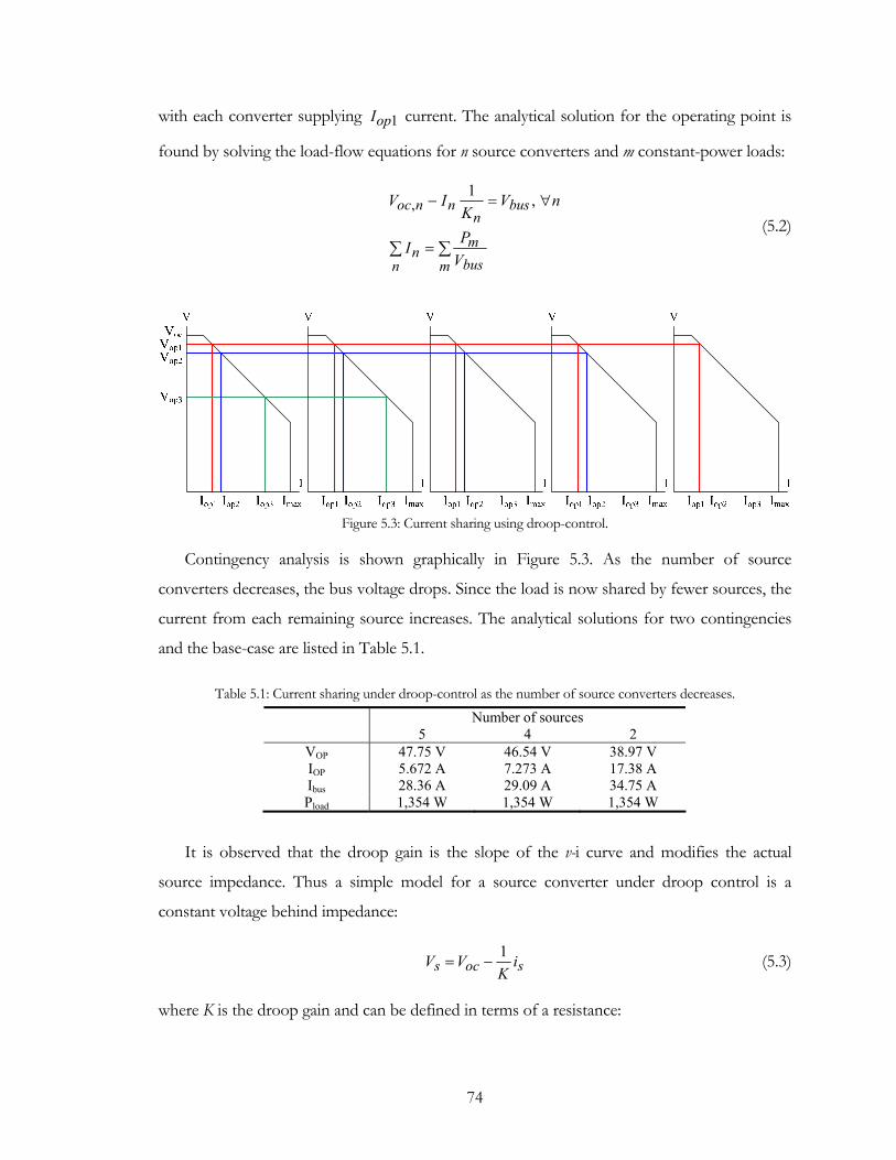
74
with each converter supplying 1opI current. The analytical solution for the operating point is
found by solving the load-flow equations for n source converters and m constant-power loads:
∑∑ =
∀=−
m busm
nn
busn
nnoc
VPI
nVK
IV ,1,
(5.2)
Figure 5.3: Current sharing using droop-control.
Contingency analysis is shown graphically in Figure 5.3. As the number of source
converters decreases, the bus voltage drops. Since the load is now shared by fewer sources, the
current from each remaining source increases. The analytical solutions for two contingencies
and the base-case are listed in Table 5.1.
Table 5.1: Current sharing under droop-control as the number of source converters decreases.
Number of sources 5 4 2
VOP 47.75 V 46.54 V 38.97 V IOP 5.672 A 7.273 A 17.38 A Ibus 28.36 A 29.09 A 34.75 A Pload 1,354 W 1,354 W 1,354 W
It is observed that the droop gain is the slope of the v-i curve and modifies the actual
source impedance. Thus a simple model for a source converter under droop control is a
constant voltage behind impedance:
socs iK
VV 1−= (5.3)
where K is the droop gain and can be defined in terms of a resistance:
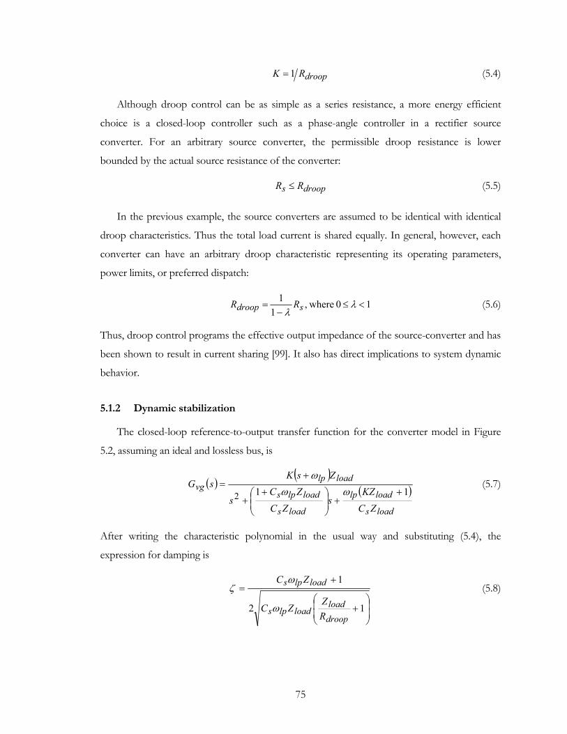
75
droopRK 1= (5.4)
Although droop control can be as simple as a series resistance, a more energy efficient
choice is a closed-loop controller such as a phase-angle controller in a rectifier source
converter. For an arbitrary source converter, the permissible droop resistance is lower
bounded by the actual source resistance of the converter:
droops RR ≤ (5.5)
In the previous example, the source converters are assumed to be identical with identical
droop characteristics. Thus the total load current is shared equally. In general, however, each
converter can have an arbitrary droop characteristic representing its operating parameters,
power limits, or preferred dispatch:
10 where,1
1<≤
−= λ
λ sdroop RR (5.6)
Thus, droop control programs the effective output impedance of the source-converter and has
been shown to result in current sharing [99]. It also has direct implications to system dynamic
behavior.
5.1.2 Dynamic stabilization
The closed-loop reference-to-output transfer function for the converter model in Figure
5.2, assuming an ideal and lossless bus, is
( )( )
( )loads
loadlp
loads
loadlps
loadlpvg
ZCKZ
sZC
ZCs
ZsKsG
112 ++⎟⎟
⎠
⎞⎜⎜⎝
⎛ ++
+=
ωω
ω (5.7)
After writing the characteristic polynomial in the usual way and substituting (5.4), the
expression for damping is
⎟⎟⎠
⎞⎜⎜⎝
⎛+
+=
12
1
droopload
loadlps
loadlps
RZ
ZC
ZC
ω
ωζ (5.8)
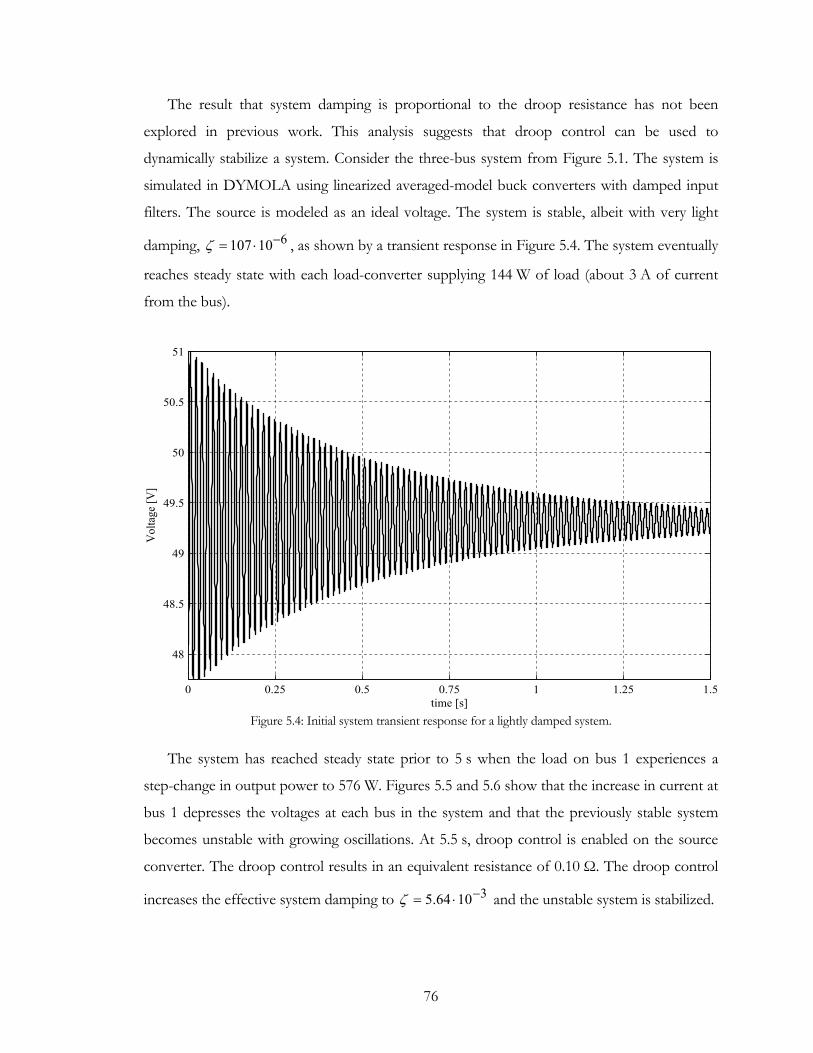
76
The result that system damping is proportional to the droop resistance has not been
explored in previous work. This analysis suggests that droop control can be used to
dynamically stabilize a system. Consider the three-bus system from Figure 5.1. The system is
simulated in DYMOLA using linearized averaged-model buck converters with damped input
filters. The source is modeled as an ideal voltage. The system is stable, albeit with very light
damping, 610107 −⋅=ζ , as shown by a transient response in Figure 5.4. The system eventually
reaches steady state with each load-converter supplying 144 W of load (about 3 A of current
from the bus).
0 0.25 0.5 0.75 1 1.25 1.5
48
48.5
49
49.5
50
50.5
51
time [s]
Vol
tage
[V]
Figure 5.4: Initial system transient response for a lightly damped system.
The system has reached steady state prior to 5 s when the load on bus 1 experiences a
step-change in output power to 576 W. Figures 5.5 and 5.6 show that the increase in current at
bus 1 depresses the voltages at each bus in the system and that the previously stable system
becomes unstable with growing oscillations. At 5.5 s, droop control is enabled on the source
converter. The droop control results in an equivalent resistance of 0.10 Ω. The droop control
increases the effective system damping to 31064.5 −⋅=ζ and the unstable system is stabilized.
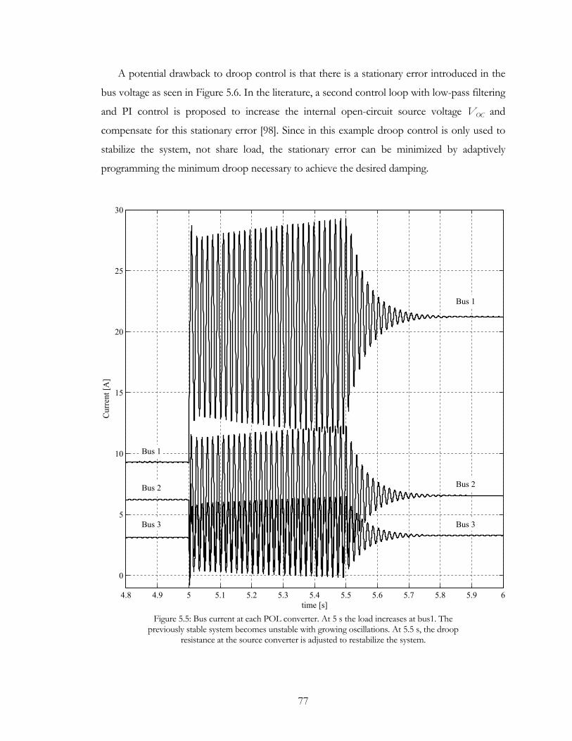
77
A potential drawback to droop control is that there is a stationary error introduced in the
bus voltage as seen in Figure 5.6. In the literature, a second control loop with low-pass filtering
and PI control is proposed to increase the internal open-circuit source voltage VOC and
compensate for this stationary error [98]. Since in this example droop control is only used to
stabilize the system, not share load, the stationary error can be minimized by adaptively
programming the minimum droop necessary to achieve the desired damping.
4.8 4.9 5 5.1 5.2 5.3 5.4 5.5 5.6 5.7 5.8 5.9 6
0
5
10
15
20
25
30
time [s]
Cur
rent
[A]
Bus 3
Bus 2
Bus 1
Bus 3
Bus 2
Bus 1
Figure 5.5: Bus current at each POL converter. At 5 s the load increases at bus1. The
previously stable system becomes unstable with growing oscillations. At 5.5 s, the droop resistance at the source converter is adjusted to restabilize the system.
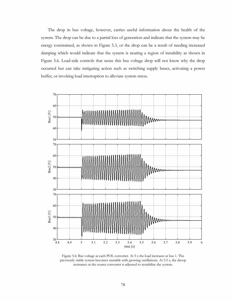
78
The drop in bus voltage, however, carries useful information about the health of the
system. The drop can be due to a partial loss of generation and indicate that the system may be
energy constrained, as shown in Figure 5.3, or the drop can be a result of needing increased
damping which would indicate that the system is nearing a region of instability as shown in
Figure 5.6. Load-side controls that sense this bus voltage drop will not know why the drop
occurred but can take mitigating action such as switching supply buses, activating a power
buffer, or invoking load interruption to alleviate system stress.
30
40
50
60
70
Bus1
[V]
30
40
50
60
70
Bus2
[V]
4.8 4.9 5 5.1 5.2 5.3 5.4 5.5 5.6 5.7 5.8 5.9 630
40
50
60
70
time [s]
Bus3
[V]
Figure 5.6: Bus voltage at each POL converter. At 5 s the load increases at bus 1. The
previously stable system becomes unstable with growing oscillations. At 5.5 s, the droop resistance at the source converter is adjusted to restabilize the system.
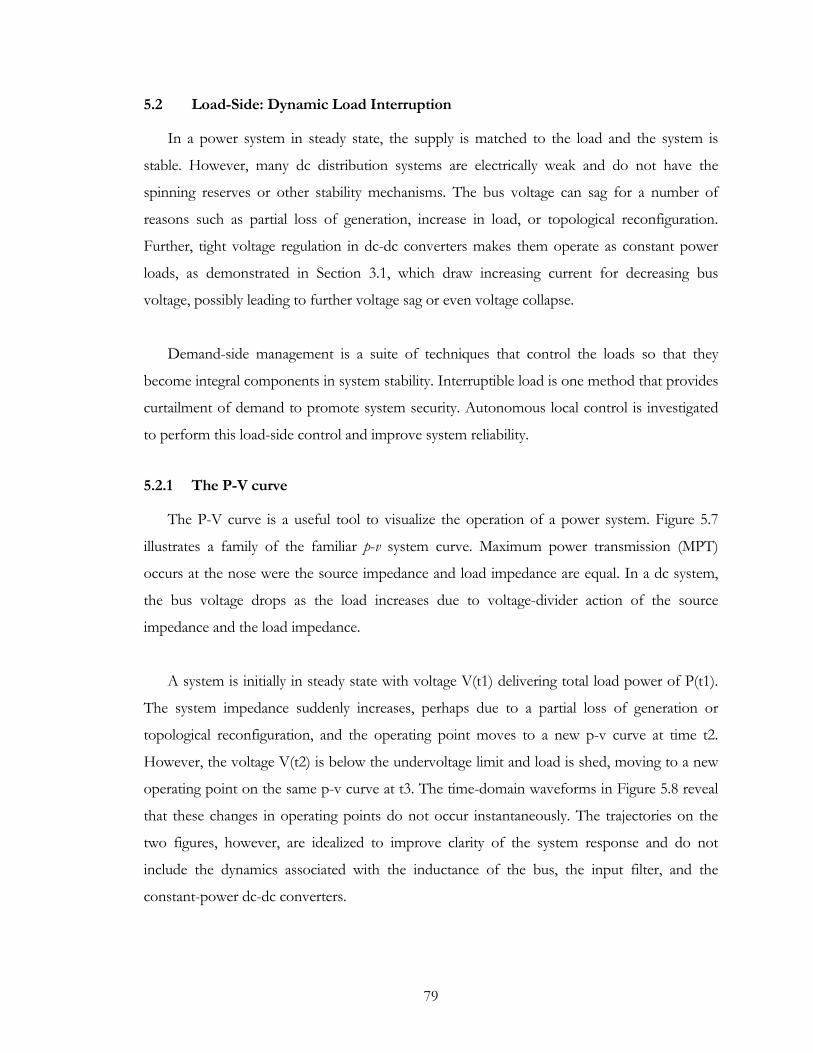
79
5.2 Load-Side: Dynamic Load Interruption
In a power system in steady state, the supply is matched to the load and the system is
stable. However, many dc distribution systems are electrically weak and do not have the
spinning reserves or other stability mechanisms. The bus voltage can sag for a number of
reasons such as partial loss of generation, increase in load, or topological reconfiguration.
Further, tight voltage regulation in dc-dc converters makes them operate as constant power
loads, as demonstrated in Section 3.1, which draw increasing current for decreasing bus
voltage, possibly leading to further voltage sag or even voltage collapse.
Demand-side management is a suite of techniques that control the loads so that they
become integral components in system stability. Interruptible load is one method that provides
curtailment of demand to promote system security. Autonomous local control is investigated
to perform this load-side control and improve system reliability.
5.2.1 The P-V curve
The P-V curve is a useful tool to visualize the operation of a power system. Figure 5.7
illustrates a family of the familiar p-v system curve. Maximum power transmission (MPT)
occurs at the nose were the source impedance and load impedance are equal. In a dc system,
the bus voltage drops as the load increases due to voltage-divider action of the source
impedance and the load impedance.
A system is initially in steady state with voltage V(t1) delivering total load power of P(t1).
The system impedance suddenly increases, perhaps due to a partial loss of generation or
topological reconfiguration, and the operating point moves to a new p-v curve at time t2.
However, the voltage V(t2) is below the undervoltage limit and load is shed, moving to a new
operating point on the same p-v curve at t3. The time-domain waveforms in Figure 5.8 reveal
that these changes in operating points do not occur instantaneously. The trajectories on the
two figures, however, are idealized to improve clarity of the system response and do not
include the dynamics associated with the inductance of the bus, the input filter, and the
constant-power dc-dc converters.
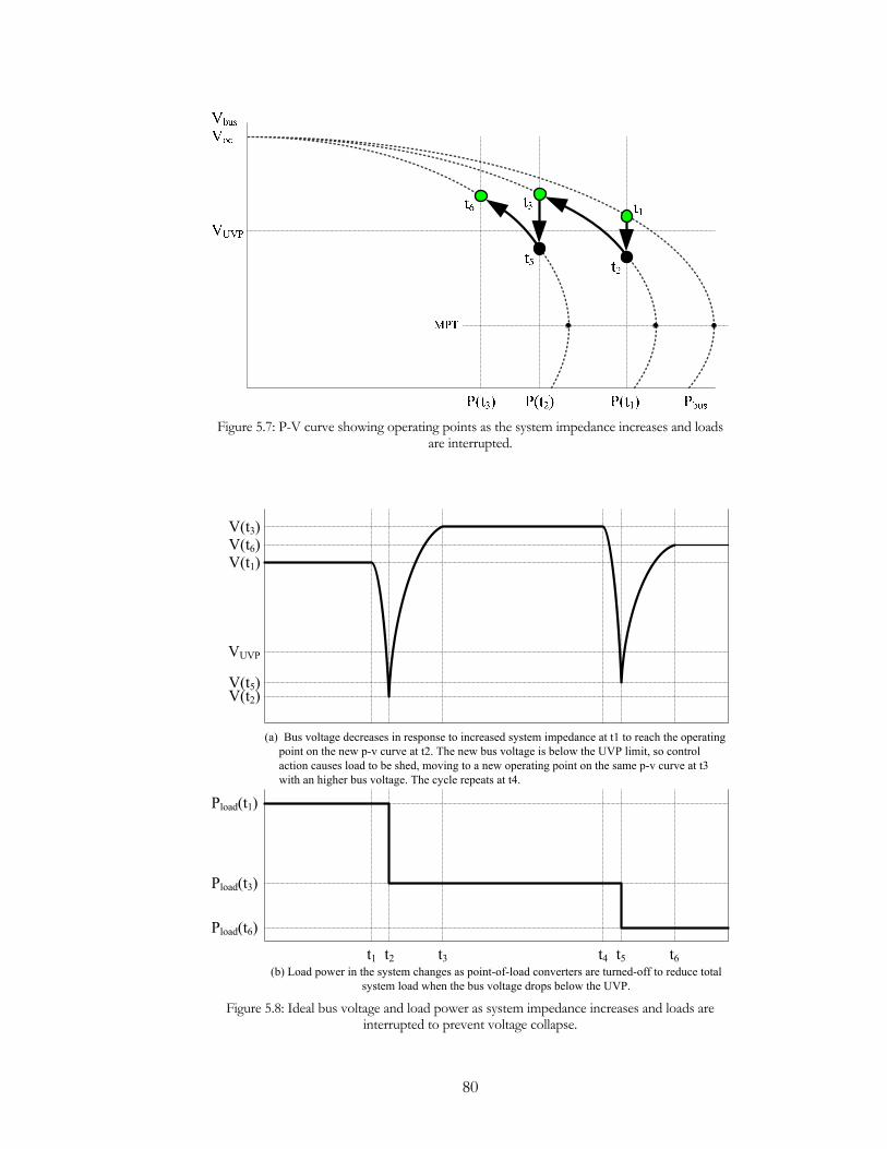
80
Figure 5.7: P-V curve showing operating points as the system impedance increases and loads
are interrupted.
V(t1)
V(t3)V(t6)
VUVP
V(t2)V(t5)
t1 t2
Pload(t1)
Pload(t3)
Pload(t6)
t6t3 t5t4
(a) Bus voltage decreases in response to increased system impedance at t1 to reach the operating point on the new p-v curve at t2. The new bus voltage is below the UVP limit, so control action causes load to be shed, moving to a new operating point on the same p-v curve at t3 with an higher bus voltage. The cycle repeats at t4.
(b) Load power in the system changes as point-of-load converters are turned-off to reduce total system load when the bus voltage drops below the UVP.
Figure 5.8: Ideal bus voltage and load power as system impedance increases and loads are interrupted to prevent voltage collapse.
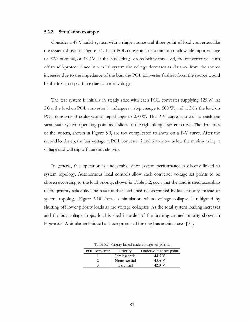
81
5.2.2 Simulation example
Consider a 48 V radial system with a single source and three point-of-load converters like
the system shown in Figure 5.1. Each POL converter has a minimum allowable input voltage
of 90% nominal, or 43.2 V. If the bus voltage drops below this level, the converter will turn
off to self-protect. Since in a radial system the voltage decreases as distance from the source
increases due to the impedance of the bus, the POL converter farthest from the source would
be the first to trip off line due to under voltage.
The test system is initially in steady state with each POL converter supplying 125 W. At
2.0 s, the load on POL converter 1 undergoes a step change to 500 W, and at 3.0 s the load on
POL converter 3 undergoes a step change to 250 W. The P-V curve is useful to track the
stead-state system operating point as it slides to the right along a system curve. The dynamics
of the system, shown in Figure 5.9, are too complicated to show on a P-V curve. After the
second load step, the bus voltage at POL converter 2 and 3 are now below the minimum input
voltage and will trip off line (not shown).
In general, this operation is undesirable since system performance is directly linked to
system topology. Autonomous local controls allow each converter voltage set points to be
chosen according to the load priority, shown in Table 5.2, such that the load is shed according
to the priority schedule. The result is that load shed is determined by load priority instead of
system topology. Figure 5.10 shows a simulation where voltage collapse is mitigated by
shutting off lower priority loads as the voltage collapses. As the total system loading increases
and the bus voltage drops, load is shed in order of the preprogrammed priority shown in
Figure 5.3. A similar technique has been proposed for ring bus architectures [10].
Table 5.2: Priority-based undervoltage set-points.
POL converter Priority Undervoltage set point 1 Semiessential 44.5 V 2 Nonessential 45.6 V 3 Essential 42.3 V
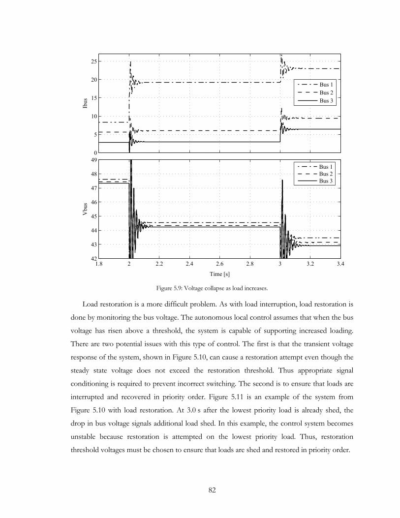
82
0
5
10
15
20
25
Ibus
1.8 2 2.2 2.4 2.6 2.8 3 3.2 3.442
43
44
45
46
47
48
49
Vbu
s
Time [s]
Bus 1Bus 2Bus 3
Bus 1Bus 2Bus 3
Figure 5.9: Voltage collapse as load increases.
Load restoration is a more difficult problem. As with load interruption, load restoration is
done by monitoring the bus voltage. The autonomous local control assumes that when the bus
voltage has risen above a threshold, the system is capable of supporting increased loading.
There are two potential issues with this type of control. The first is that the transient voltage
response of the system, shown in Figure 5.10, can cause a restoration attempt even though the
steady state voltage does not exceed the restoration threshold. Thus appropriate signal
conditioning is required to prevent incorrect switching. The second is to ensure that loads are
interrupted and recovered in priority order. Figure 5.11 is an example of the system from
Figure 5.10 with load restoration. At 3.0 s after the lowest priority load is already shed, the
drop in bus voltage signals additional load shed. In this example, the control system becomes
unstable because restoration is attempted on the lowest priority load. Thus, restoration
threshold voltages must be chosen to ensure that loads are shed and restored in priority order.
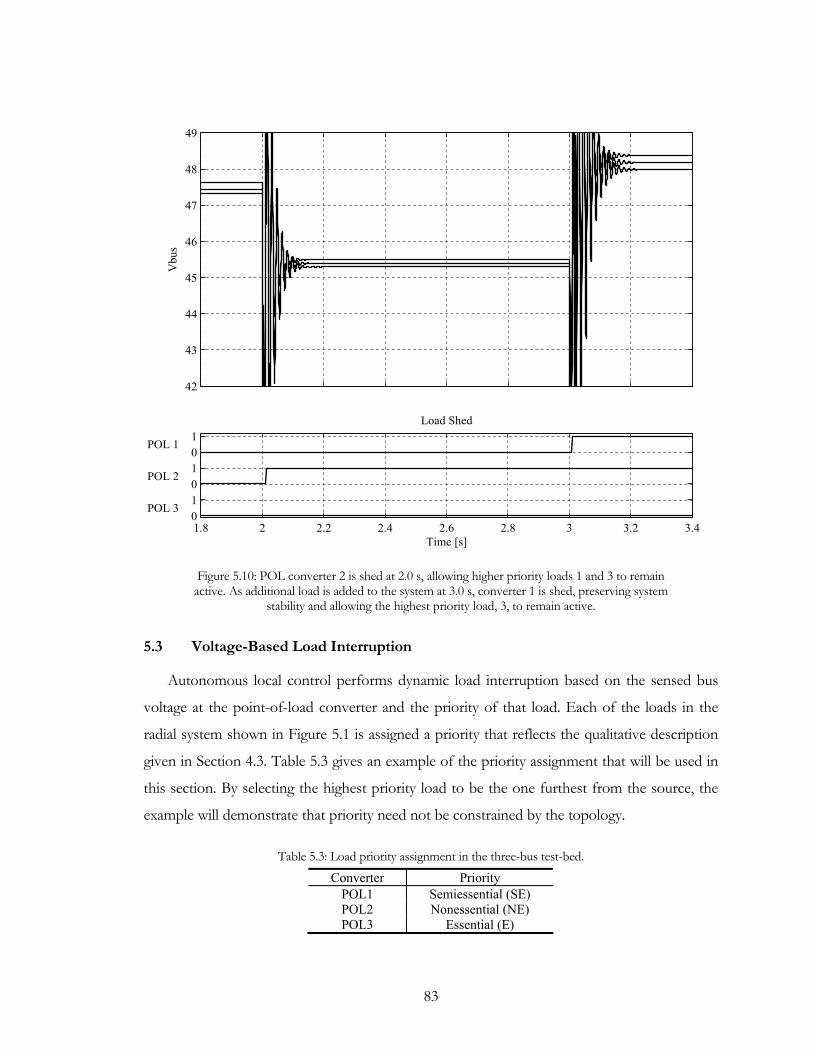
83
42
43
44
45
46
47
48
49
Vbu
s
1.8 2 2.2 2.4 2.6 2.8 3 3.2 3.4010101
Load Shed
Time [s]
POL 1
POL 2
POL 3
Figure 5.10: POL converter 2 is shed at 2.0 s, allowing higher priority loads 1 and 3 to remain
active. As additional load is added to the system at 3.0 s, converter 1 is shed, preserving system stability and allowing the highest priority load, 3, to remain active.
5.3 Voltage-Based Load Interruption
Autonomous local control performs dynamic load interruption based on the sensed bus
voltage at the point-of-load converter and the priority of that load. Each of the loads in the
radial system shown in Figure 5.1 is assigned a priority that reflects the qualitative description
given in Section 4.3. Table 5.3 gives an example of the priority assignment that will be used in
this section. By selecting the highest priority load to be the one furthest from the source, the
example will demonstrate that priority need not be constrained by the topology.
Table 5.3: Load priority assignment in the three-bus test-bed.
Converter Priority POL1 Semiessential (SE) POL2 Nonessential (NE) POL3 Essential (E)
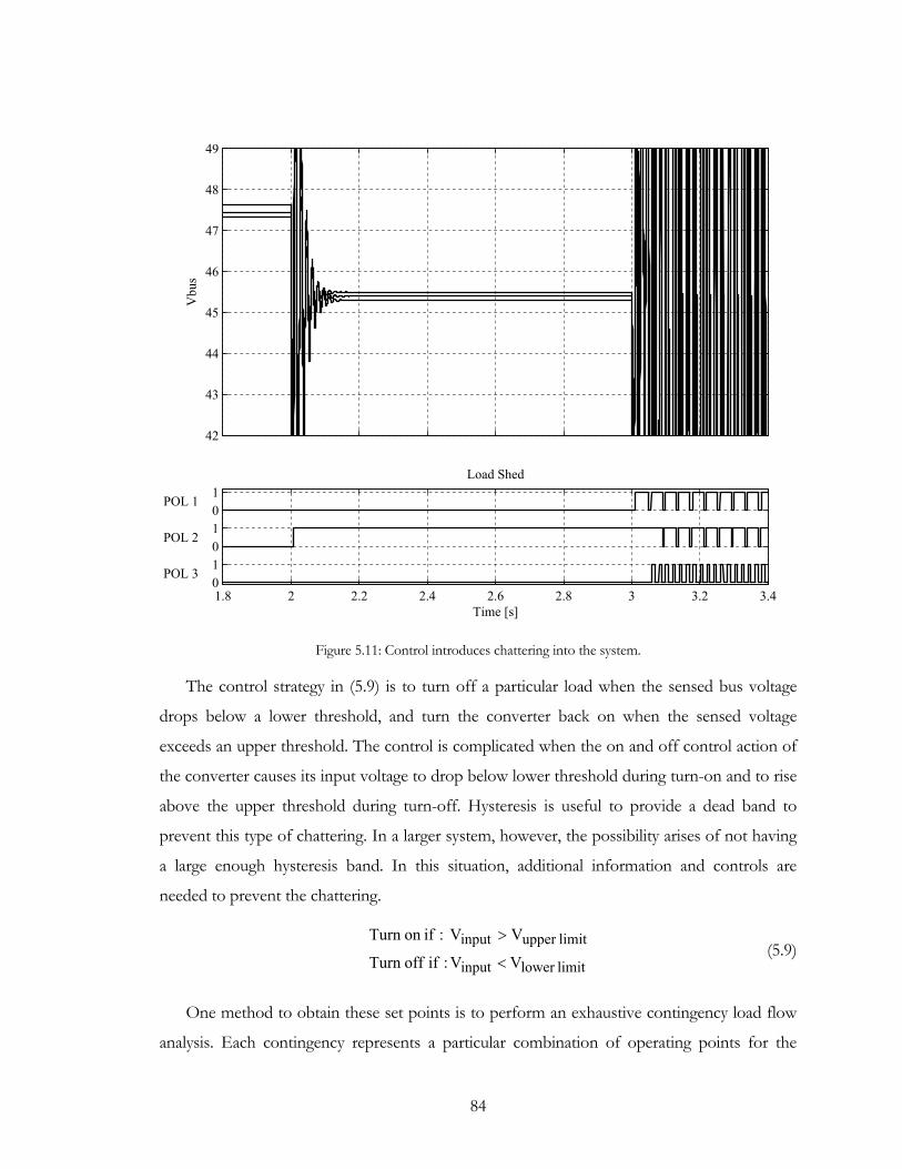
84
42
43
44
45
46
47
48
49
Vbu
s
1.8 2 2.2 2.4 2.6 2.8 3 3.2 3.4010101
Load Shed
Time [s]
POL 1
POL 2
POL 3
Figure 5.11: Control introduces chattering into the system.
The control strategy in (5.9) is to turn off a particular load when the sensed bus voltage
drops below a lower threshold, and turn the converter back on when the sensed voltage
exceeds an upper threshold. The control is complicated when the on and off control action of
the converter causes its input voltage to drop below lower threshold during turn-on and to rise
above the upper threshold during turn-off. Hysteresis is useful to provide a dead band to
prevent this type of chattering. In a larger system, however, the possibility arises of not having
a large enough hysteresis band. In this situation, additional information and controls are
needed to prevent the chattering.
limitlower input
limitupper inputV V :if offTurn
VV :ifon Turn
<
> (5.9)
One method to obtain these set points is to perform an exhaustive contingency load flow
analysis. Each contingency represents a particular combination of operating points for the
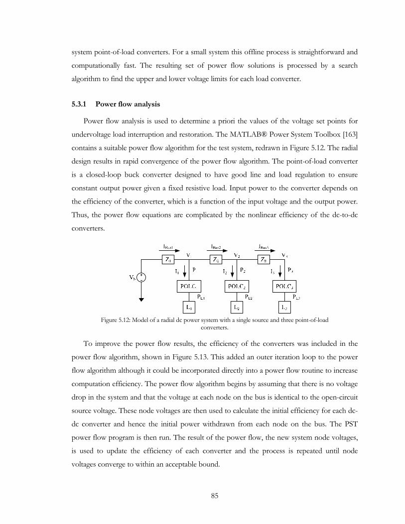
85
system point-of-load converters. For a small system this offline process is straightforward and
computationally fast. The resulting set of power flow solutions is processed by a search
algorithm to find the upper and lower voltage limits for each load converter.
5.3.1 Power flow analysis
Power flow analysis is used to determine a priori the values of the voltage set points for
undervoltage load interruption and restoration. The MATLAB® Power System Toolbox [163]
contains a suitable power flow algorithm for the test system, redrawn in Figure 5.12. The radial
design results in rapid convergence of the power flow algorithm. The point-of-load converter
is a closed-loop buck converter designed to have good line and load regulation to ensure
constant output power given a fixed resistive load. Input power to the converter depends on
the efficiency of the converter, which is a function of the input voltage and the output power.
Thus, the power flow equations are complicated by the nonlinear efficiency of the dc-to-dc
converters.
Figure 5.12: Model of a radial dc power system with a single source and three point-of-load
converters.
To improve the power flow results, the efficiency of the converters was included in the
power flow algorithm, shown in Figure 5.13. This added an outer iteration loop to the power
flow algorithm although it could be incorporated directly into a power flow routine to increase
computation efficiency. The power flow algorithm begins by assuming that there is no voltage
drop in the system and that the voltage at each node on the bus is identical to the open-circuit
source voltage. These node voltages are then used to calculate the initial efficiency for each dc-
dc converter and hence the initial power withdrawn from each node on the bus. The PST
power flow program is then run. The result of the power flow, the new system node voltages,
is used to update the efficiency of each converter and the process is repeated until node
voltages converge to within an acceptable bound.
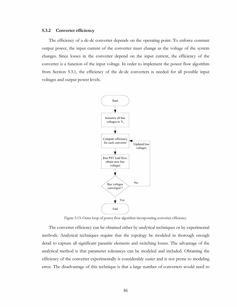
86
5.3.2 Converter efficiency
The efficiency of a dc-dc converter depends on the operating point. To enforce constant
output power, the input current of the converter must change as the voltage of the system
changes. Since losses in the converter depend on the input current, the efficiency of the
converter is a function of the input voltage. In order to implement the power flow algorithm
from Section 5.3.1, the efficiency of the dc-dc converters is needed for all possible input
voltages and output power levels.
Initialize all bus voltages to Vs
Compute efficiency for each converter
Run PST load flow, obtain new bus
voltages
Start
End
Bus voltages converged ?
No
Yes
Updated bus voltages
Figure 5.13: Outer loop of power flow algorithm incorporating converter efficiency.
The converter efficiency can be obtained either by analytical techniques or by experimental
methods. Analytical techniques require that the topology be modeled in thorough enough
detail to capture all significant parasitic elements and switching losses. The advantage of the
analytical method is that parameter tolerances can be modeled and included. Obtaining the
efficiency of the converter experimentally is considerably easier and is not prone to modeling
error. The disadvantage of this technique is that a large number of converters would need to

87
be sampled in a practical application in order to incorporate parameter variations. However,
this information is usually known already for quality control purposes.
The efficiency of the prototype converter was experimentally obtained at two power levels
that were chosen to span the range of expected load. The MATLAB curve fit toolbox
(cftool) was used to fit a third-order Gaussian curve (Gauss3) with a 95% confidence
bound to the data. The general form of the third-order Gaussian curve is
( )⎟⎟⎟
⎠
⎞
⎜⎜⎜
⎝
⎛
⎟⎟⎠
⎞⎜⎜⎝
⎛ −−+
⎟⎟⎟
⎠
⎞
⎜⎜⎜
⎝
⎛
⎟⎟⎠
⎞⎜⎜⎝
⎛ −−+
⎟⎟⎟
⎠
⎞
⎜⎜⎜
⎝
⎛
⎟⎟⎠
⎞⎜⎜⎝
⎛ −−=
2
33
3
2
22
2
2
11
1 expexpexpc
bVa
cbVa
cbVaVη (5.10)
The variable V is the sensed input bus voltage to the point-of-load converter, η is the
efficiency. The parameters for the curve at each power level are listed in Table 5.4. A plot of
the experimental data overlaid with the fit curve is shown in Figure 5.14 and verifies good
agreement.
Table 5.4: Coefficients for third-order Gaussian curve fit with 95% confidence. Converter Output Curve fit parameter 5 V, 18 W 5 V, 43 W
a1 30.64 67240.0 b1 -103.9 -115.5 c1 53.12 32.8 a2 0.636 0.8092 b2 20.87 12.45 c2 28.7 182.2 a3 0.5538 0.006936 b3 55.44 14.03 c3 24.52 8.126
An approximation to the actual efficiency of a converter can be found by interpolating
between the efficiency curves taken at two fixed output power levels, ( )PVP ,1η and
( )PVP ,2η . The interpolated efficiency curve is found by forming the convex hull of these two
efficiency curves:
( ) ( ) ( ) ⎟⎟⎠
⎞⎜⎜⎝
⎛−−
⋅+⎟⎟⎠
⎞⎜⎜⎝
⎛−−
−⋅=121
121' ,1,, 21 PP
PPPVPPPPPVPV PP ηηη (5.11)
The result is an equation that relates the converter efficiency to the input voltage and load
power and is suitable for incorporation into the power flow analysis to improve accuracy.
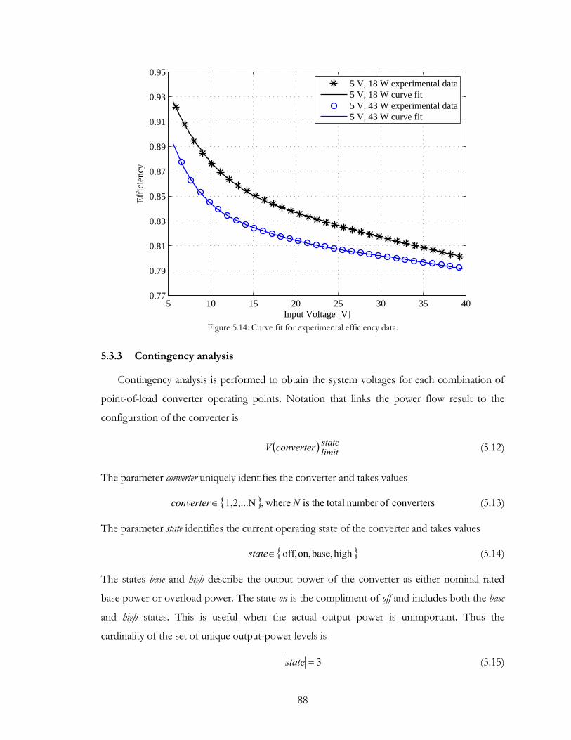
88
5 10 15 20 25 30 35 400.77
0.79
0.81
0.83
0.85
0.87
0.89
0.91
0.93
0.95
Input Voltage [V]
Eff
icie
ncy
5 V, 18 W experimental data5 V, 18 W curve fit5 V, 43 W experimental data5 V, 43 W curve fit
Figure 5.14: Curve fit for experimental efficiency data.
5.3.3 Contingency analysis
Contingency analysis is performed to obtain the system voltages for each combination of
point-of-load converter operating points. Notation that links the power flow result to the
configuration of the converter is
( ) statelimitconverterV (5.12)
The parameter converter uniquely identifies the converter and takes values
converters ofnumber total theis where,1,2,...N Nconverter∈ (5.13)
The parameter state identifies the current operating state of the converter and takes values
highbase,on,off,∈state (5.14)
The states base and high describe the output power of the converter as either nominal rated
base power or overload power. The state on is the compliment of off and includes both the base
and high states. This is useful when the actual output power is unimportant. Thus the
cardinality of the set of unique output-power levels is
3=state (5.15)
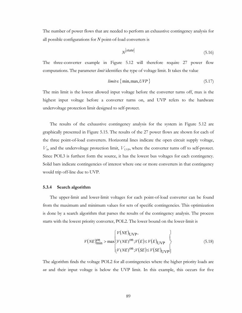
89
The number of power flows that are needed to perform an exhaustive contingency analysis for
all possible configurations for N point-of-load converters is
stateN (5.16)
The three-converter example in Figure 5.12 will therefore require 27 power flow
computations. The parameter limit identifies the type of voltage limit. It takes the value
UVPlimit max,min,∈ (5.17)
The min limit is the lowest allowed input voltage before the converter turns off, max is the
highest input voltage before a converter turns on, and UVP refers to the hardware
undervoltage protection limit designed to self-protect.
The results of the exhaustive contingency analysis for the system in Figure 5.12 are
graphically presented in Figure 5.15. The results of the 27 power flows are shown for each of
the three point-of-load converters. Horizontal lines indicate the open circuit supply voltage,
VS, and the undervoltage protection limit, VUVP, where the converter turns off to self-protect.
Since POL3 is furthest form the source, it has the lowest bus voltages for each contingency.
Solid bars indicate contingencies of interest where one or more converters in that contingency
would trip off-line due to UVP.
5.3.4 Search algorithm
The upper-limit and lower-limit voltages for each point-of-load converter can be found
from the maximum and minimum values for sets of specific contingencies. This optimization
is done by a search algorithm that parses the results of the contingency analysis. The process
starts with the lowest priority converter, POL2. The lower bound on the lower-limit is
( )( )
( ) ( )( ) ( ) ⎪
⎪⎭
⎪⎪⎬
⎫
⎪⎪⎩
⎪⎪⎨
⎧
≤
≤>
UVPon
UVPonUVP
onmin
;)(
;)(
,
max
SEVSEVNEV
EVEVNEV
NEV
NEV (5.18)
The algorithm finds the voltage POL2 for all contingencies where the higher priority loads are
on and their input voltage is below the UVP limit. In this example, this occurs for five
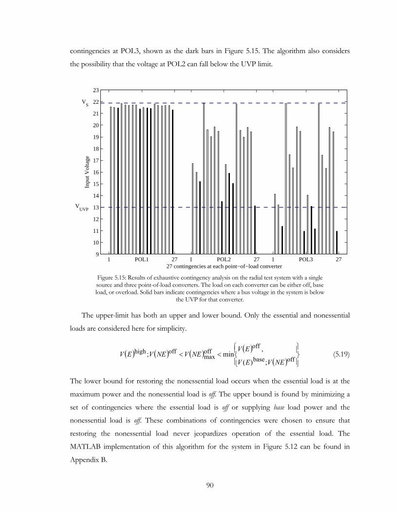
90
contingencies at POL3, shown as the dark bars in Figure 5.15. The algorithm also considers
the possibility that the voltage at POL2 can fall below the UVP limit.
1 POL1 27 1 POL2 27 1 POL3 279
10
11
12
13
14
15
16
17
18
19
20
21
22
23
27 contingencies at each point−of−load converter
Inpu
t Vol
tage
VUVP
VS
Figure 5.15: Results of exhaustive contingency analysis on the radial test system with a single source and three point-of-load converters. The load on each converter can be either off, base load, or overload. Solid bars indicate contingencies where a bus voltage in the system is below
the UVP for that converter.
The upper-limit has both an upper and lower bound. Only the essential and nonessential
loads are considered here for simplicity.
( ) ( ) ( ) ( )( ) ⎪⎭
⎪⎬⎫
⎪⎩
⎪⎨⎧
<<offbase
offoffmax
offhigh
;)(
,min;
NEVEV
EVNEVNEVEV (5.19)
The lower bound for restoring the nonessential load occurs when the essential load is at the
maximum power and the nonessential load is off. The upper bound is found by minimizing a
set of contingencies where the essential load is off or supplying base load power and the
nonessential load is off. These combinations of contingencies were chosen to ensure that
restoring the nonessential load never jeopardizes operation of the essential load. The
MATLAB implementation of this algorithm for the system in Figure 5.12 can be found in
Appendix B.

91
5.3.5 Experimental results
A reduced-power prototype of the single supply, three load system in Figure 5.1 was
constructed using a closed-loop buck converter and PIC-based controller. Design details can
be found in Appendix A. The supply voltage was regulated for constant 22 V. The output of
each buck converter was 5 V with a base load of 30 W and high-output load of 36 W. Signal
conditioning in the autonomous local controller is designed to allow quick response to changes
in the bus voltage, but prevent false load interruption due to bus dynamics. The priority of
each load and the result of the contingency search algorithm are listed in Table 5.5. The actual
values used in the controller differ slightly from those computed due to parameter differences
between the model and actual circuit elements and resolution limitations in the controller.
Since POL3 is considered to be essential, the controller is programmed with 0 V as both the
upper-limit and lower-limit to ensure that it will always be energized.
Table 5.5: Load priority assignment in the three-bus test-bed.
POL1 POL2 POL3 Priority Semiessential Nonessential Essential Computed from power flow Lower-limit minimum 15.524 V Upper-limit minimum 18.966 V Upper-limit maximum 19.480 V Actual values in controller Lower-limit 18.820 V 16.140 V 0 V Upper-limit 19.000 V 19.575 V 0 V
The results of three tests are presented here. The first will demonstrate the system
response to increased loading without using dynamic load interruption. The second will use
the same loading conditions but with dynamic load interruption enabled. The last will show
more complicated system response with multiple loads changing. The bus voltages are low-
pass filtered in the accompanying figures to aid visualization of the system response and
control action.
The operation of the system without dynamic load interruption is shown in Figure 5.16.
The system is originally in steady state and each point-of-load converter is supplying the base
load. At approximately 0.4 s, the load at POL3, the essential load, increases, as indicated by the
step change on the load step variable. The new steady-state voltage at POL3 is below the UVP
92
limit. The load is reduced back to the base level at about 1.4 s to prevent the converter from
turning off to self-protect. The system then returns to the original condition.
121314151617181920212223
Vbu
sSystem Voltages
POL2
POL1
Vs
POL3
UVP
010101
Load Shed
POL3
POL2
POL1
0 0.2 0.4 0.6 0.8 1 1.2 1.4 1.6 1.8010101
Time [s]
Load Step
POL3
POL2
POL1
Figure 5.16: System voltages drop in response to an increase in loading at POL3. Since the new
terminal voltage for POL3 is below the UVP, it will trip off-line to self-protect.
Next, the dynamic load controller is enabled and the load profile is repeated. When the bus
voltage at the nonessential load, POL2, decreases below the lower-limit, the controller
interrupts the load as shown in Figure 5.17. This action reduces system loading which results
in higher bus voltage and guarantees that the higher priority loads remain energized. Just after
1.2 s, the load on POL3 decreases to the original level. The bus voltage rises as load is
removed from the system. The dynamic load controller at POL2 senses that the voltage is now
above the upper-limit and restores operation of the load, returning the system to the original
configuration.
Figure 5.18 illustrates dynamic load interruption for more complicated sequence of load
changes. Initially only POL2 is on (the high load shed for POL1 and POL3 is because they
were manually turned off.) The bus voltages for POL2 and POL3 are the same since there is
no current flowing in the last bus segment. At 1.1 s, POL3 turns on (the load shed signal goes
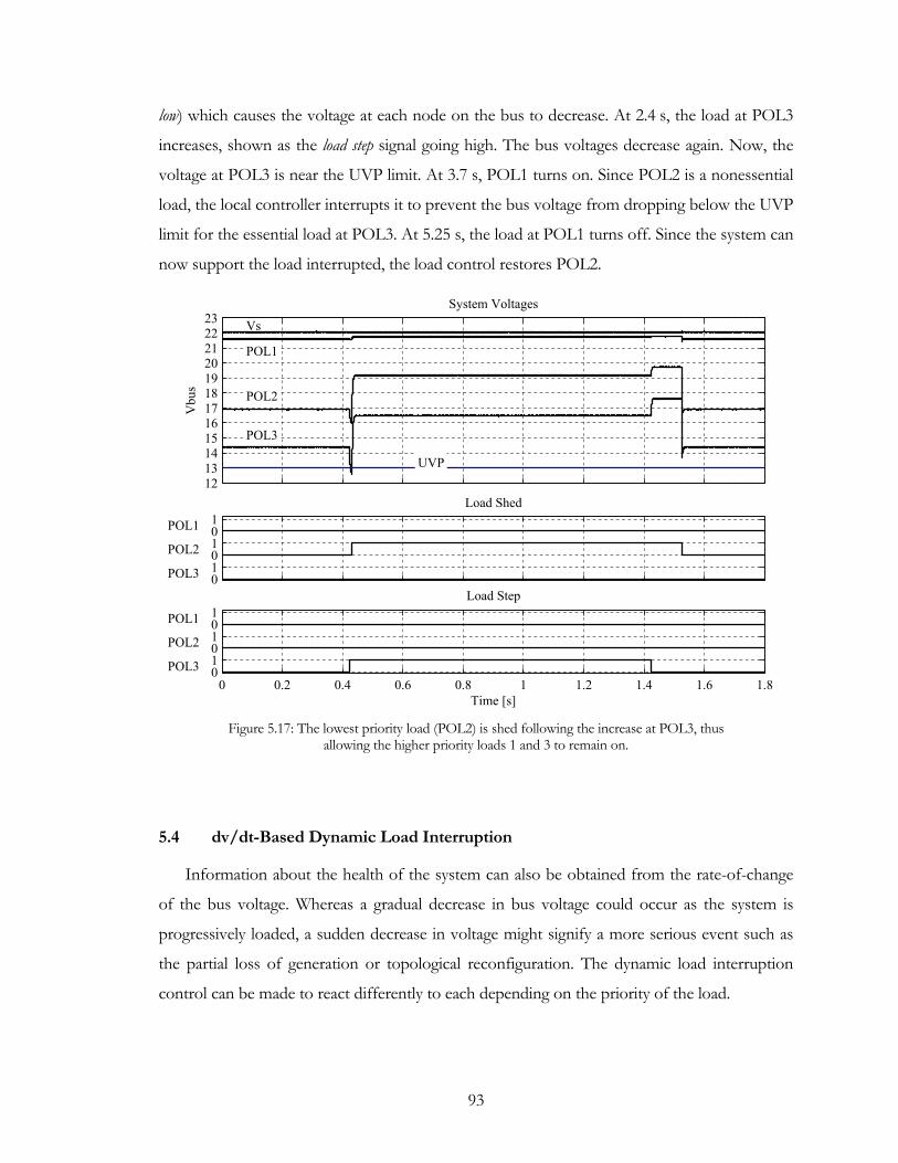
93
low) which causes the voltage at each node on the bus to decrease. At 2.4 s, the load at POL3
increases, shown as the load step signal going high. The bus voltages decrease again. Now, the
voltage at POL3 is near the UVP limit. At 3.7 s, POL1 turns on. Since POL2 is a nonessential
load, the local controller interrupts it to prevent the bus voltage from dropping below the UVP
limit for the essential load at POL3. At 5.25 s, the load at POL1 turns off. Since the system can
now support the load interrupted, the load control restores POL2.
121314151617181920212223
Vbu
s
System Voltages
POL3
POL2
POL1
Vs
UVP
010101
Load Shed
POL3
POL2
POL1
0 0.2 0.4 0.6 0.8 1 1.2 1.4 1.6 1.8010101
Time [s]
Load Step
POL3
POL2
POL1
Figure 5.17: The lowest priority load (POL2) is shed following the increase at POL3, thus
allowing the higher priority loads 1 and 3 to remain on.
5.4 dv/dt-Based Dynamic Load Interruption
Information about the health of the system can also be obtained from the rate-of-change
of the bus voltage. Whereas a gradual decrease in bus voltage could occur as the system is
progressively loaded, a sudden decrease in voltage might signify a more serious event such as
the partial loss of generation or topological reconfiguration. The dynamic load interruption
control can be made to react differently to each depending on the priority of the load.
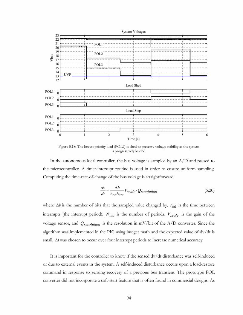
94
121314151617181920212223
Vbu
s
System Voltages
POL3
POL2
POL1
UVP
010101
Load Shed
POL3
POL2
POL1
0 1 2 3 4 5 6010101
Time [s]
Load Step
POL3
POL2
POL1
Figure 5.18: The lowest priority load (POL2) is shed to preserve voltage stability as the system
is progressively loaded.
In the autonomous local controller, the bus voltage is sampled by an A/D and passed to
the microcontroller. A timer-interrupt routine is used in order to ensure uniform sampling.
Computing the time-rate-of-change of the bus voltage is straightforward:
resolutionscale QVNtb
dtdv
⋅∆
=intint
(5.20)
where b∆ is the number of bits that the sampled value changed by, intt is the time between
interrupts (the interrupt period), intN is the number of periods, scaleV is the gain of the
voltage sensor, and resolutionQ is the resolution in mV/bit of the A/D converter. Since the
algorithm was implemented in the PIC using integer math and the expected value of dv/dt is
small, t∆ was chosen to occur over four interrupt periods to increase numerical accuracy.
It is important for the controller to know if the sensed dv/dt disturbance was self-induced
or due to external events in the system. A self-induced disturbance occurs upon a load-restore
command in response to sensing recovery of a previous bus transient. The prototype POL
converter did not incorporate a soft-start feature that is often found in commercial designs. As
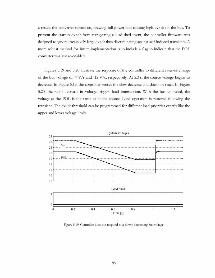
95
a result, the converter turned on, drawing full power and causing high dv/dt on the bus. To
prevent the startup dv/dt from retriggering a load-shed event, the controller firmware was
designed to ignore excessively large dv/dt thus discriminating against self-induced transients. A
more robust method for future implementation is to include a flag to indicate that the POL
converter was just re-enabled.
Figures 5.19 and 5.20 illustrate the response of the controller to different rates-of-change
of the bus voltage of -7 V/s and -12 V/s, respectively. At 2.3 s, the source voltage begins to
decrease. In Figure 5.19, the controller senses the slow decrease and does not react. In Figure
5.20, the rapid decrease in voltage triggers load interruption. With the bus unloaded, the
voltage at the POL is the same as at the source. Load operation is restored following the
transient. The dv/dt threshold can be programmed for different load priorities exactly like the
upper and lower voltage limits.
15
16
17
18
19
20
21
22
23System Voltages
POL
Vs
0 0.2 0.4 0.6 0.8 1 1.20
1
Time [s]
Load Shed
Figure 5.19: Controller does not respond to a slowly decreasing bus voltage.
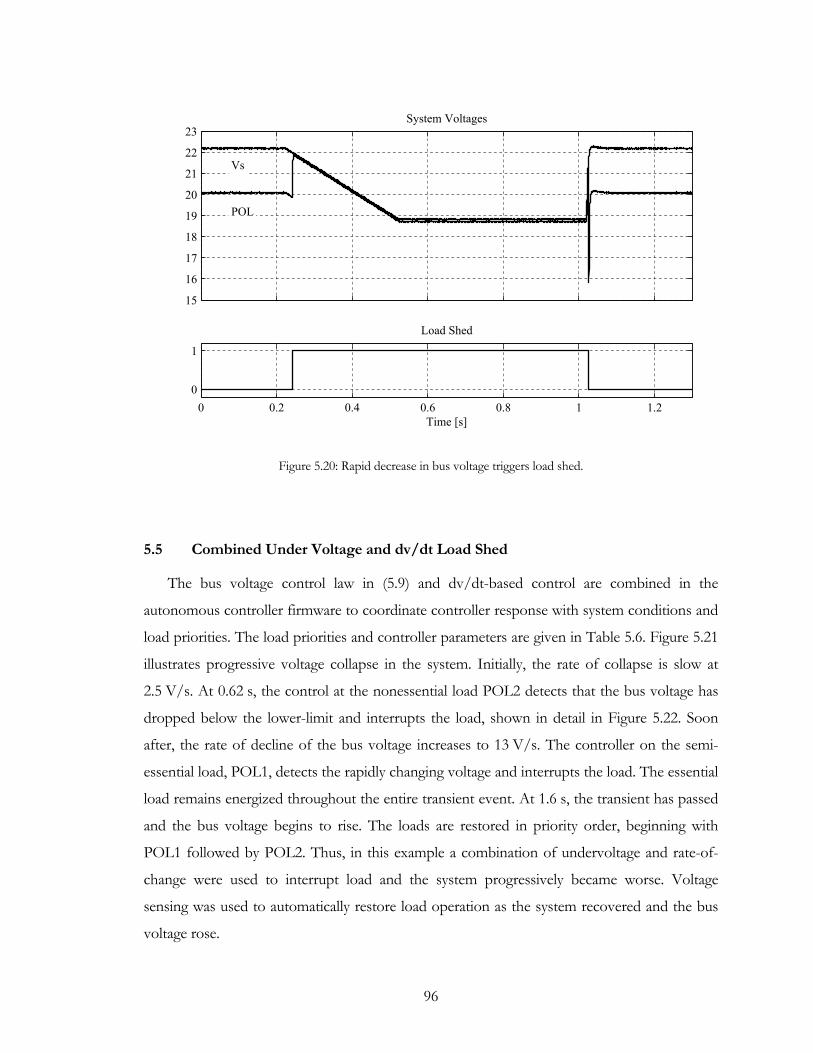
96
15
16
17
18
19
20
21
22
23System Voltages
Vs
POL
0 0.2 0.4 0.6 0.8 1 1.20
1
Time [s]
Load Shed
Figure 5.20: Rapid decrease in bus voltage triggers load shed.
5.5 Combined Under Voltage and dv/dt Load Shed
The bus voltage control law in (5.9) and dv/dt-based control are combined in the
autonomous controller firmware to coordinate controller response with system conditions and
load priorities. The load priorities and controller parameters are given in Table 5.6. Figure 5.21
illustrates progressive voltage collapse in the system. Initially, the rate of collapse is slow at
2.5 V/s. At 0.62 s, the control at the nonessential load POL2 detects that the bus voltage has
dropped below the lower-limit and interrupts the load, shown in detail in Figure 5.22. Soon
after, the rate of decline of the bus voltage increases to 13 V/s. The controller on the semi-
essential load, POL1, detects the rapidly changing voltage and interrupts the load. The essential
load remains energized throughout the entire transient event. At 1.6 s, the transient has passed
and the bus voltage begins to rise. The loads are restored in priority order, beginning with
POL1 followed by POL2. Thus, in this example a combination of undervoltage and rate-of-
change were used to interrupt load and the system progressively became worse. Voltage
sensing was used to automatically restore load operation as the system recovered and the bus
voltage rose.
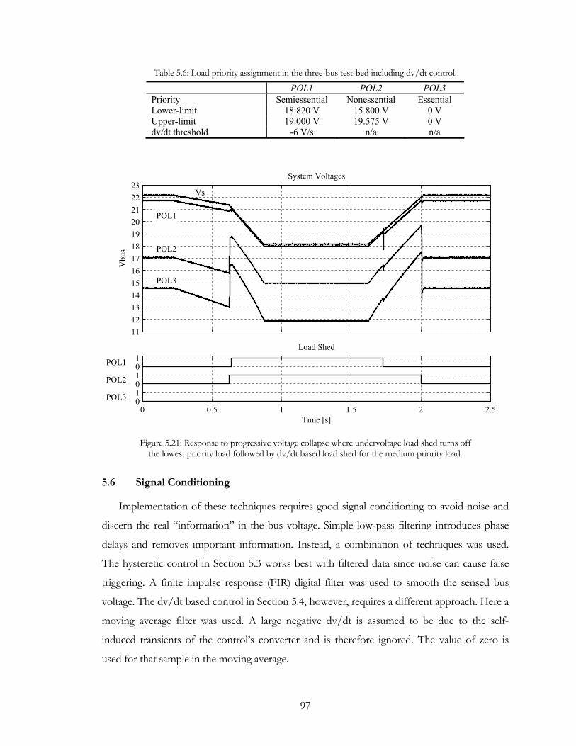
97
Table 5.6: Load priority assignment in the three-bus test-bed including dv/dt control.
POL1 POL2 POL3 Priority Semiessential Nonessential Essential Lower-limit 18.820 V 15.800 V 0 V Upper-limit 19.000 V 19.575 V 0 V dv/dt threshold -6 V/s n/a n/a
11121314151617181920212223
Vbu
s
System Voltages
POL2
POL1
POL3
Vs
0 0.5 1 1.5 2 2.5010101
Time [s]
Load Shed
POL3
POL2
POL1
Figure 5.21: Response to progressive voltage collapse where undervoltage load shed turns off
the lowest priority load followed by dv/dt based load shed for the medium priority load.
5.6 Signal Conditioning
Implementation of these techniques requires good signal conditioning to avoid noise and
discern the real “information” in the bus voltage. Simple low-pass filtering introduces phase
delays and removes important information. Instead, a combination of techniques was used.
The hysteretic control in Section 5.3 works best with filtered data since noise can cause false
triggering. A finite impulse response (FIR) digital filter was used to smooth the sensed bus
voltage. The dv/dt based control in Section 5.4, however, requires a different approach. Here a
moving average filter was used. A large negative dv/dt is assumed to be due to the self-
induced transients of the control’s converter and is therefore ignored. The value of zero is
used for that sample in the moving average.
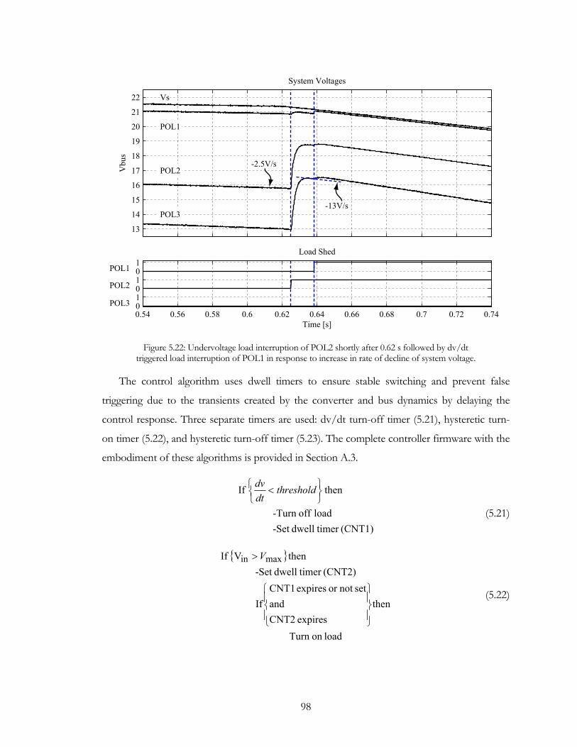
98
13
14
15
16
17
18
19
20
21
22
Vbu
s
System Voltages
POL2
POL3
POL1
Vs
0.54 0.56 0.58 0.6 0.62 0.64 0.66 0.68 0.7 0.72 0.74010101
Time [s]
Load Shed
POL3
POL2
POL1
-2.5V/s
-13V/s
Figure 5.22: Undervoltage load interruption of POL2 shortly after 0.62 s followed by dv/dt
triggered load interruption of POL1 in response to increase in rate of decline of system voltage.
The control algorithm uses dwell timers to ensure stable switching and prevent false
triggering due to the transients created by the converter and bus dynamics by delaying the
control response. Three separate timers are used: dv/dt turn-off timer (5.21), hysteretic turn-
on timer (5.22), and hysteretic turn-off timer (5.23). The complete controller firmware with the
embodiment of these algorithms is provided in Section A.3.
(CNT1) timer dwell-Set
load off -Turn
then If⎭⎬⎫
⎩⎨⎧ < threshold
dtdv
(5.21)
load on Turn
thenexpires CNT2
andsetnot or expires CNT1
If
(CNT2) timer dwell-Set thenV If maxin
⎪⎭
⎪⎬
⎫
⎪⎩
⎪⎨
⎧
>V
(5.22)

99
load on Turn
thenexpires CNT_offIf(CNT_off) timer dwell-Set
thenV If maxin V<
(5.23)
5.7 Bilevel Programming
The problem of finding the dynamic load interruption voltage limits can be generalized
through the framework of mathematical programming, with results suitable for extension to
arbitrarily large systems. A bilevel program, a sub-subset of mathematical programming, has a
hierarchy of two optimization problems; the variables of the outer program are constrained by
the optimal solution of the inner program [164, 165]. The max-min problem, one particular
bilevel program, has been studied recently within the context of the power system “Terrorist
Threat Problem” [166-168] and represents a formulation where the outer and inner objective
functions are different.
The objective of dynamic load interruption is to ensure that the highest priority loads
remain energized. A bilevel program is useful here in order to maximize the number of loads
that can operate subject to the constraints of priority, system network flow, and undervoltage
protection. Consider an objective function which represents the performance score for the
system:
∑ jj xc (5.24)
where
load for the signal onInterrupti
load theofPriority th
j
thj
jx
jc
=
= (5.25)
Let
⎩⎨⎧
∈nedunconstrai ,1dinterrupte,0
jx (5.26)
indicate that the load has either been interrupted or is unconstrained. If the load is
unconstrained, the load is free to operate in any output power state, including off. The loads are
multiplied by a weighting coefficient based on priority:

100
essentialessentialsemiessentialnon ccc << −− (5.27)
Since the control objective is to ensure that loads are allowed to operate in priority order, the
weighting coefficients are chosen such that that the sum of lower priority weighting
coefficients is less than the higher priority weighting coefficient. A candidate function to
generate the weighting factors for an arbitrary system is
levelspriority ...2,1,2 1 Mmc m =∈ − (5.28)
The objective of the program is to find the control parameter Vmin that results from the
bilevel problem:
∑ jjuxviV
xcminmax,,,min
(5.29)
subject to the network constraints:
∑=
−
=
−=
N
jkjj
jjjj
iibus
Zibusvv 1
(5.30)
where jZ is the thj bus impedance, N is the number of loads, and 0v is the prescribed
source voltage, the thj load power:
( ) jjjjj ivupx = (5.31)
and the voltage constraints to keep loads from turning off due to undervoltage
( ) 0,1min >−≤− MxMvV jjj (5.32)
The auxiliary variables are defines as
load by the system thefrom thdrawnCurrent wi
load at the system thefrom drawnPower with
bus theincurrent Bus
load theof voltageBus
,, load; theOperation
thj
thj
thj
thj
jth
j
ji
jp
jibus
jv
highbaseoffuju
=
=
=
=
∈=
(5.33)
101
To verify the optimization formulation, consider the case when the voltage at the jth load is
greater than the lower-limit. The load is unconstrained, so by definition 1 =jx . Therefore,
from (5.29),
jj
jj vVvV ≤⇒≤− minmin 0 (5.34)
which confirms the desired operation. Now, consider the case where load interruption occurs.
By definition, 0 =jx . From (5.29)
MvVtsM jj ≤−<>∃ min0..0 (5.35)
The objective of the inner minimization function is to find the worst-case performance
index where the most important loads do not have sufficient voltage to turn on by the control
law in (5.9). The objective of the outer optimization is to maximize the value of the worst-case
configuration performance index. Thus the max-min optimization results in the best, worst-
case operation. The result of the bilevel program in (5.26) – (5.30) is the lower-limit for load
interruption in the control law (5.9). A similar formulation can be written to obtain the upper-
limit for load restoration.
5.8 Impedance-Based Online Measurements
The methods discussed so far are suitable when the upper and lower limits for dynamic
load interruption can be computed off-line. Techniques for on-line measurement of the
impedance ratio at the POL-bus interface, suitable for integration into point-of-load
converters, have been proposed as a method to detect system faults [169, 170]. These
techniques are useful here because the measured impedance relationship can be used as a
signal to sense the health of the system.
Figure 5.23 shows the bus voltages of the system in Figure 5.1 responding to a change in
load at POL2 and POL3. The dashed lines show that the system behavior, without dynamic
load interruption, leads to voltage collapse. The bus voltage at POLC3 is below the minimum
input voltage and the converter falls out of regulation. The solid lines show the system
response when load interruption is enabled. POL2, the nonessential load, turns off when the
sensed bus voltage drops below the threshold value, which arrests voltage collapse. Figure 5.24

102
shows the ratio of POL converter input impedance to the Thevenin system impedance for
each converter. Without load interruption control, this ratio for POLC3 drops below unity, a
violation of the Middlebrook criterion for stability. Enabling the load interruption prevents the
ratio from becoming less than unity.
An interesting problem left for future work is to study the linkage between the impedance
relationship at each point-of-load converter and the system voltage. Figures 5.23 and 5.24
suggest that measuring the ratio on-line can provide another way that autonomous local
controls can sense the condition of the system and interrupt load to prevent voltage collapse.
5.9 Conclusions
This chapter examined autonomous local controllers in a single-bus system. On the supply
side, droop control is used to share current among many source converters. The small-signal
characteristics of droop control were shown here to add damping to a system. Changes in the
bus voltage, whether because of changes in supply or the need to damp the system, convey
valuable information to controls distributed in the system.
On the load side, intelligent dynamic load interruption is presented as a local control that
stabilizes the system by reducing demand. A challenge to it is determining the values for the
undervoltage and load-restoration set points. An algorithm based on an exhaustive load-flow
analysis was used for the demonstration system. The problem was later generalized as a bilevel
mathematical program that is suitable for an arbitrarily sized system. It was shown that
dynamic load control changes the effective system impedance. Monitoring this impedance is a
candidate for an on-line technique to initiate dynamic load control and is proposed for future
work.
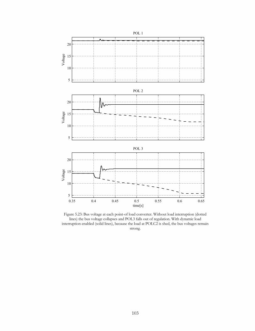
103
5
10
15
20
Vol
tage
POL 1
5
10
15
20
Vol
tage
POL 2
0.35 0.4 0.45 0.5 0.55 0.6 0.655
10
15
20
Vol
tage
POL 3
time[s]
Figure 5.23: Bus voltage at each point-of load converter. Without load interruption (dotted lines) the bus voltage collapses and POL3 falls out of regulation. With dynamic load
interruption enabled (solid lines), because the load at POLC2 is shed, the bus voltages remain strong.
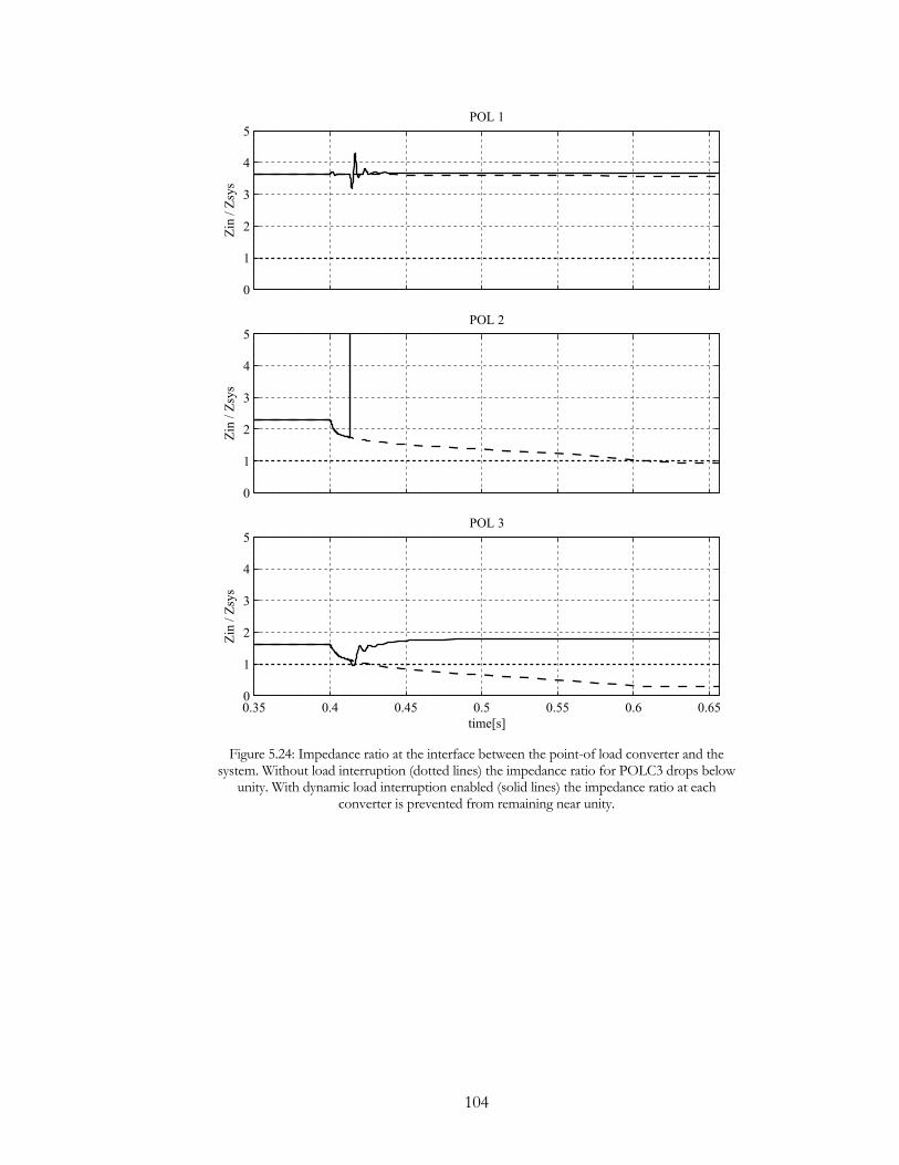
104
0
1
2
3
4
5
Zin
/ Zsy
s
POL 1
0
1
2
3
4
5
Zin
/ Zsy
s
POL 2
0.35 0.4 0.45 0.5 0.55 0.6 0.650
1
2
3
4
5
Zin
/ Zsy
s
POL 3
time[s]
Figure 5.24: Impedance ratio at the interface between the point-of load converter and the system. Without load interruption (dotted lines) the impedance ratio for POLC3 drops below
unity. With dynamic load interruption enabled (solid lines) the impedance ratio at each converter is prevented from remaining near unity.
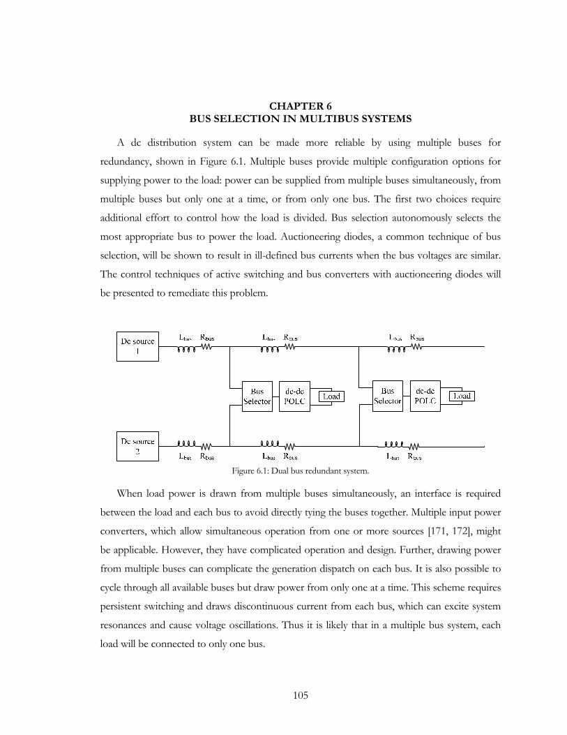
105
CHAPTER 6 BUS SELECTION IN MULTIBUS SYSTEMS
A dc distribution system can be made more reliable by using multiple buses for
redundancy, shown in Figure 6.1. Multiple buses provide multiple configuration options for
supplying power to the load: power can be supplied from multiple buses simultaneously, from
multiple buses but only one at a time, or from only one bus. The first two choices require
additional effort to control how the load is divided. Bus selection autonomously selects the
most appropriate bus to power the load. Auctioneering diodes, a common technique of bus
selection, will be shown to result in ill-defined bus currents when the bus voltages are similar.
The control techniques of active switching and bus converters with auctioneering diodes will
be presented to remediate this problem.
Figure 6.1: Dual bus redundant system.
When load power is drawn from multiple buses simultaneously, an interface is required
between the load and each bus to avoid directly tying the buses together. Multiple input power
converters, which allow simultaneous operation from one or more sources [171, 172], might
be applicable. However, they have complicated operation and design. Further, drawing power
from multiple buses can complicate the generation dispatch on each bus. It is also possible to
cycle through all available buses but draw power from only one at a time. This scheme requires
persistent switching and draws discontinuous current from each bus, which can excite system
resonances and cause voltage oscillations. Thus it is likely that in a multiple bus system, each
load will be connected to only one bus.

106
This chapter focuses on a bus selection strategy where the load draws power from the bus
with the higher voltage. This results in lower current and thus lower losses. Discrete
auctioneering diodes, an inexpensive solution for OR’ing multiple supply buses, are a common
solution. The diode action automatically and passively chooses the bus with the highest voltage
to supply the load, yet it provides instantaneous transfer if that voltage suddenly drops. It also
prevents reverse current, or back-feeding. The voltage of each bus depends on the impedance
of the topology configuration and the operating point of the system. Simply diode-connecting
the point-of-load converter to each bus results in indeterminate current flow when the buses
have similar voltages. The result is that both buses end up supplying the load, but the current-
sharing is uncontrolled. Thus, auctioneering diodes is not the best choice.
A more sophisticated solution is to actively control which bus supplies the load. Forward
conducting, bidirectional blocking switches allow full control of the bus selection process yet
retain the reverse current protection that the diodes provided. A simple control strategy is to
select the bus with the higher voltage which mimics the ideal auctioneering diode but avoids
the indeterminate current sharing when bus voltages are close. This simple control, however, is
subject to chattering, as the switching-induced transient conditions excite the dynamics of the
bus and cause the bus voltages to oscillate. The control challenge becomes how to prevent
excessive switching and constant perturbation of the system.
Hybrid system theory provides a framework to prevent chattering through “slow
switching” [173]. Dwell time is examined as a technique to inhibit switching due to the system
transient behavior. With excessive switching prevented, the bus selector can then
autonomously choose the configuration which results in the highest voltage supplied to the
load.
6.1 Bus Selection: Auctioneering Diodes
Consider the dual bus redundant system supplying a resistive load shown in Figure 6.2
where each bus is represented as an ideal voltage source with some series resistance. The first
order analysis of the circuit assumes a constant voltage-drop approximation for the diodes.
Applying Kirchoff’s voltage law to the left and right loops results in the branch equations:
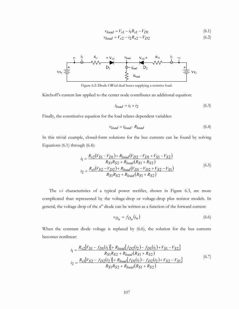
107
1111 Dssload VRiVv −−= (6.1) 2222 Dssload VRiVv −−= (6.2)
Figure 6.2: Diode OR’ed dual buses supplying a resistive load.
Kirchoff’s current law applied to the center node contributes an additional equation:
21 iiiload += (6.3)
Finally, the constitutive equation for the load relates dependent variables:
loadloadload Riv ⋅= (6.4)
In this trivial example, closed-form solutions for the bus currents can be found by solving
Equations (6.1) through (6.4):
( ) ( )( )
( ) ( )( )2121
12212212
21212112112
1
SSloadSSSSDDloadDSs
SSloadSSSSDDloadDSs
RRRRRVVVVRVVRi
RRRRRVVVVRVVRi
++−+−+−
=
++−+−+−
=
(6.5)
The v-i characteristics of a typical power rectifier, shown in Figure 6.3, are more
complicated than represented by the voltage-drop or voltage-drop plus resistor models. In
general, the voltage drop of the nth diode can be written as a function of the forward current:
( )nDD ifv nn = (6.6)
When the constant diode voltage is replaced by (6.6), the solution for the bus currents
becomes nonlinear:
( )[ ] ( ) ( )[ ]( )
( )[ ] ( ) ( )[ ]( )2121
12221122212
21212111221112
1
SSloadSSSSDDloadDSs
SSloadSSSSDDloadDSs
RRRRRVVififRifVRi
RRRRRVVififRifVRi
++−+−+−
=
++−+−+−
=
(6.7)
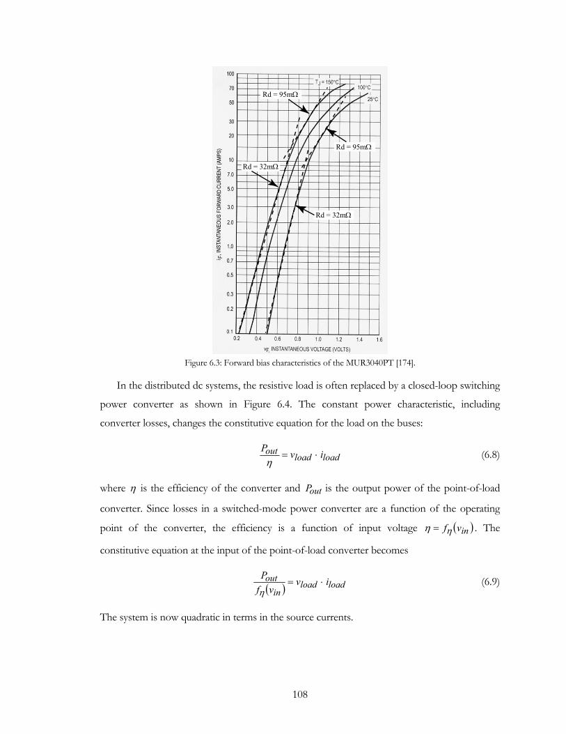
108
Rd = 32mΩ
Rd = 32mΩ
Rd = 95mΩ
Rd = 95mΩ
Figure 6.3: Forward bias characteristics of the MUR3040PT [174].
In the distributed dc systems, the resistive load is often replaced by a closed-loop switching
power converter as shown in Figure 6.4. The constant power characteristic, including
converter losses, changes the constitutive equation for the load on the buses:
loadloadout ivP
⋅=η
(6.8)
where η is the efficiency of the converter and outP is the output power of the point-of-load
converter. Since losses in a switched-mode power converter are a function of the operating
point of the converter, the efficiency is a function of input voltage ( )invfηη = . The
constitutive equation at the input of the point-of-load converter becomes
( ) loadloadin
out ivvf
P⋅=
η (6.9)
The system is now quadratic in terms in the source currents.
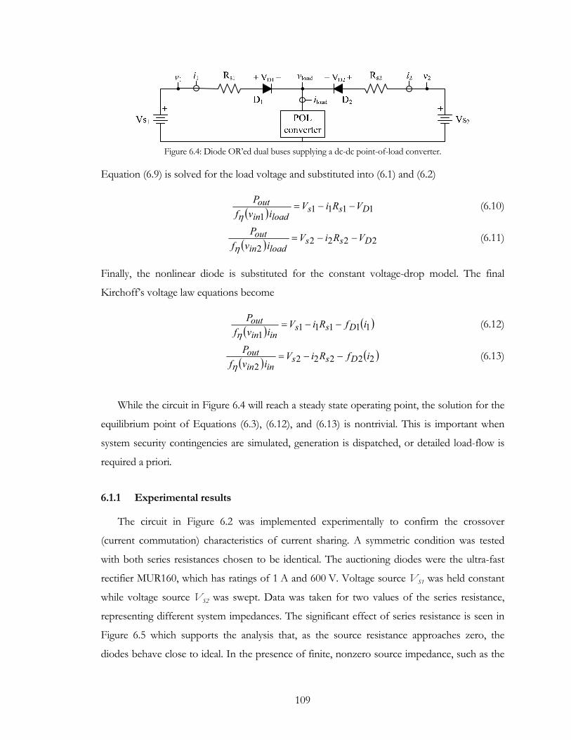
109
Figure 6.4: Diode OR’ed dual buses supplying a dc-dc point-of-load converter.
Equation (6.9) is solved for the load voltage and substituted into (6.1) and (6.2)
( ) 11111
Dssloadin
out VRiVivf
P−−=
η (6.10)
( ) 22222
Dssloadin
out VRiVivf
P−−=
η (6.11)
Finally, the nonlinear diode is substituted for the constant voltage-drop model. The final
Kirchoff’s voltage law equations become
( ) ( )111111
ifRiVivf
PDss
ininout −−=
η (6.12)
( ) ( )222222
ifRiVivf
PDss
ininout −−=
η (6.13)
While the circuit in Figure 6.4 will reach a steady state operating point, the solution for the
equilibrium point of Equations (6.3), (6.12), and (6.13) is nontrivial. This is important when
system security contingencies are simulated, generation is dispatched, or detailed load-flow is
required a priori.
6.1.1 Experimental results
The circuit in Figure 6.2 was implemented experimentally to confirm the crossover
(current commutation) characteristics of current sharing. A symmetric condition was tested
with both series resistances chosen to be identical. The auctioning diodes were the ultra-fast
rectifier MUR160, which has ratings of 1 A and 600 V. Voltage source VS1 was held constant
while voltage source VS2 was swept. Data was taken for two values of the series resistance,
representing different system impedances. The significant effect of series resistance is seen in
Figure 6.5 which supports the analysis that, as the source resistance approaches zero, the
diodes behave close to ideal. In the presence of finite, nonzero source impedance, such as the
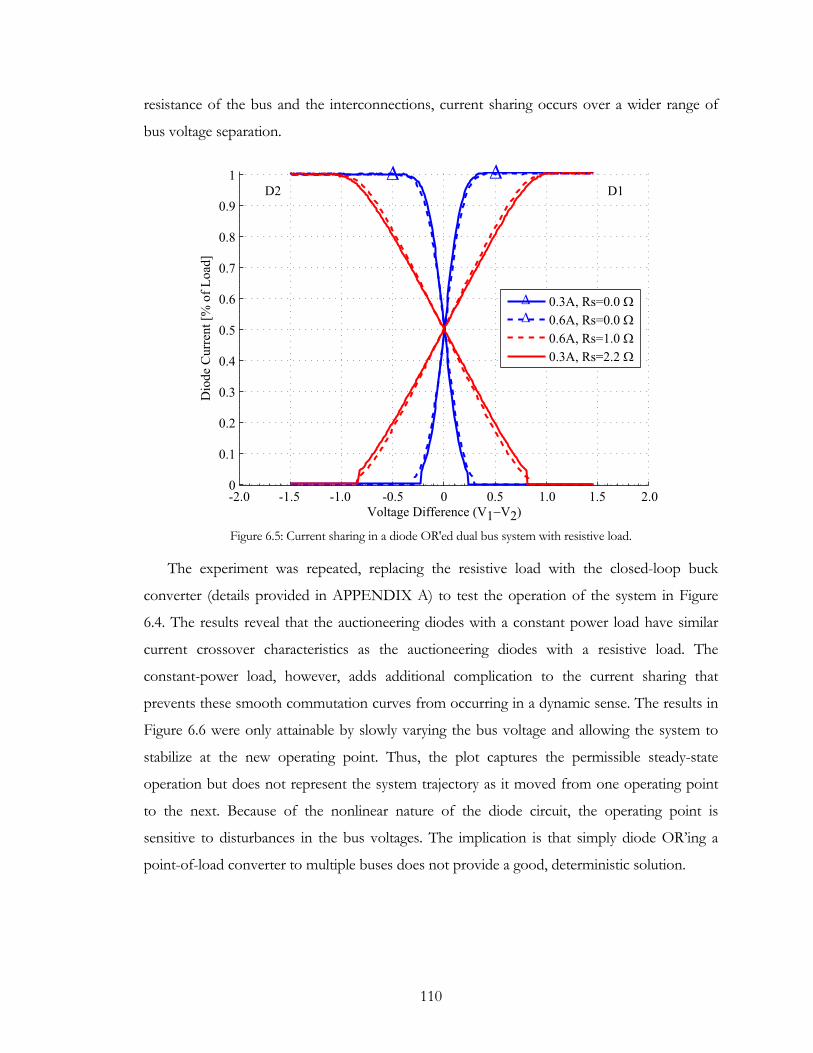
110
resistance of the bus and the interconnections, current sharing occurs over a wider range of
bus voltage separation.
-2.0 -1.5 -1.0 -0.5 0 0.5 1.0 1.5 2.00
0.1
0.2
0.3
0.4
0.5
0.6
0.7
0.8
0.9
1
Voltage Difference (V1−V2)
Dio
de
Curr
ent
[% o
f L
oad
]D2 D1
0.3A, Rs=0.0 Ω
0.6A, Rs=0.0 Ω
0.6A, Rs=1.0 Ω
0.3A, Rs=2.2 Ω
∆ ∆
∆
∆
Figure 6.5: Current sharing in a diode OR'ed dual bus system with resistive load.
The experiment was repeated, replacing the resistive load with the closed-loop buck
converter (details provided in APPENDIX A) to test the operation of the system in Figure
6.4. The results reveal that the auctioneering diodes with a constant power load have similar
current crossover characteristics as the auctioneering diodes with a resistive load. The
constant-power load, however, adds additional complication to the current sharing that
prevents these smooth commutation curves from occurring in a dynamic sense. The results in
Figure 6.6 were only attainable by slowly varying the bus voltage and allowing the system to
stabilize at the new operating point. Thus, the plot captures the permissible steady-state
operation but does not represent the system trajectory as it moved from one operating point
to the next. Because of the nonlinear nature of the diode circuit, the operating point is
sensitive to disturbances in the bus voltages. The implication is that simply diode OR’ing a
point-of-load converter to multiple buses does not provide a good, deterministic solution.
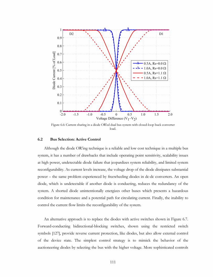
111
-2.0 -1.5 -1.0 -0.5 0 0.5 1.0 1.5 2.00
0.1
0.2
0.3
0.4
0.5
0.6
0.7
0.8
0.9
1
Voltage Difference (V1−V2)
Dio
de
Curr
ent
[% o
f L
oad
]
D1D2
0.5A, Rs=0.0 Ω
1.0A, Rs=0.0 Ω
0.5A, Rs=1.1 Ω
1.0A, Rs=1.1 Ω
∆
∆
∆ ∆
Figure 6.6: Current sharing in a diode OR'ed dual bus system with closed-loop buck converter
load.
6.2 Bus Selection: Active Control
Although the diode OR’ing technique is a reliable and low cost technique in a multiple bus
system, it has a number of drawbacks that include operating point sensitivity, scalability issues
at high power, undetectable diode failure that jeopardizes system reliability, and limited system
reconfigurability. As current levels increase, the voltage drop of the diode dissipates substantial
power – the same problem experienced by freewheeling diodes in dc-dc converters. An open
diode, which is undetectable if another diode is conducting, reduces the redundancy of the
system. A shorted diode unintentionally energizes other buses which presents a hazardous
condition for maintenance and a potential path for circulating current. Finally, the inability to
control the current flow limits the reconfigurability of the system.
An alternative approach is to replace the diodes with active switches shown in Figure 6.7.
Forward-conducting bidirectional-blocking switches, shown using the restricted switch
symbols [127], provide reverse current protection, like diodes, but also allow external control
of the device state. The simplest control strategy is to mimick the behavior of the
auctioneering diodes by selecting the bus with the higher voltage. More sophisticated controls
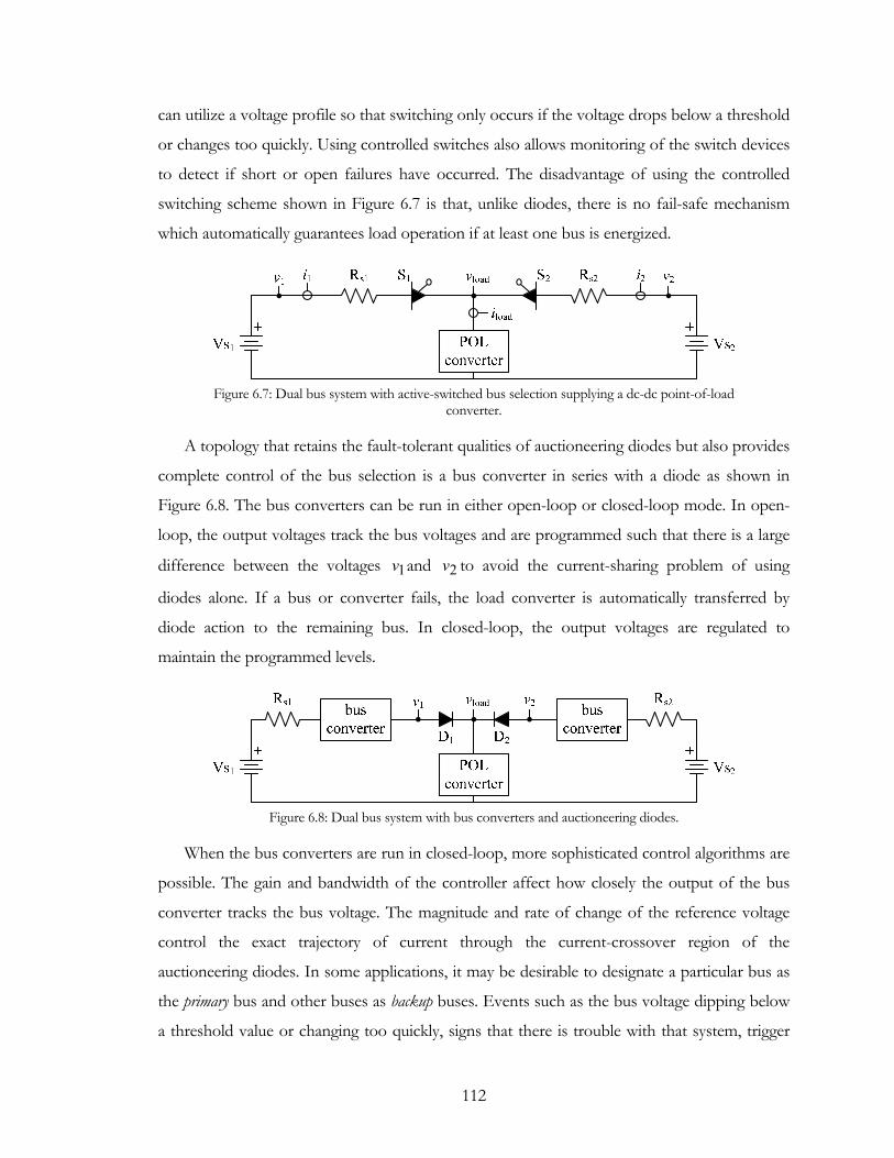
112
can utilize a voltage profile so that switching only occurs if the voltage drops below a threshold
or changes too quickly. Using controlled switches also allows monitoring of the switch devices
to detect if short or open failures have occurred. The disadvantage of using the controlled
switching scheme shown in Figure 6.7 is that, unlike diodes, there is no fail-safe mechanism
which automatically guarantees load operation if at least one bus is energized.
Figure 6.7: Dual bus system with active-switched bus selection supplying a dc-dc point-of-load
converter.
A topology that retains the fault-tolerant qualities of auctioneering diodes but also provides
complete control of the bus selection is a bus converter in series with a diode as shown in
Figure 6.8. The bus converters can be run in either open-loop or closed-loop mode. In open-
loop, the output voltages track the bus voltages and are programmed such that there is a large
difference between the voltages 1v and 2v to avoid the current-sharing problem of using
diodes alone. If a bus or converter fails, the load converter is automatically transferred by
diode action to the remaining bus. In closed-loop, the output voltages are regulated to
maintain the programmed levels.
Figure 6.8: Dual bus system with bus converters and auctioneering diodes.
When the bus converters are run in closed-loop, more sophisticated control algorithms are
possible. The gain and bandwidth of the controller affect how closely the output of the bus
converter tracks the bus voltage. The magnitude and rate of change of the reference voltage
control the exact trajectory of current through the current-crossover region of the
auctioneering diodes. In some applications, it may be desirable to designate a particular bus as
the primary bus and other buses as backup buses. Events such as the bus voltage dipping below
a threshold value or changing too quickly, signs that there is trouble with that system, trigger
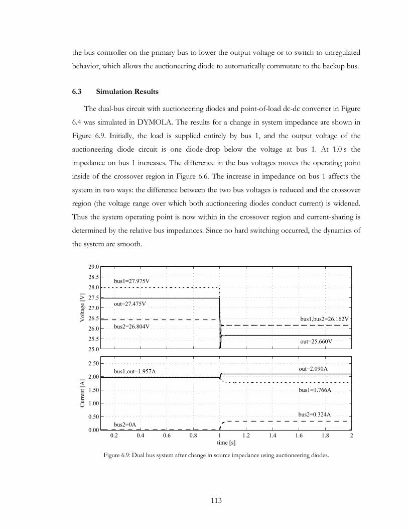
113
the bus controller on the primary bus to lower the output voltage or to switch to unregulated
behavior, which allows the auctioneering diode to automatically commutate to the backup bus.
6.3 Simulation Results
The dual-bus circuit with auctioneering diodes and point-of-load dc-dc converter in Figure
6.4 was simulated in DYMOLA. The results for a change in system impedance are shown in
Figure 6.9. Initially, the load is supplied entirely by bus 1, and the output voltage of the
auctioneering diode circuit is one diode-drop below the voltage at bus 1. At 1.0 s the
impedance on bus 1 increases. The difference in the bus voltages moves the operating point
inside of the crossover region in Figure 6.6. The increase in impedance on bus 1 affects the
system in two ways: the difference between the two bus voltages is reduced and the crossover
region (the voltage range over which both auctioneering diodes conduct current) is widened.
Thus the system operating point is now within in the crossover region and current-sharing is
determined by the relative bus impedances. Since no hard switching occurred, the dynamics of
the system are smooth.
25.0
25.5
26.0
26.5
27.0
27.5
28.0
28.5
29.0
Vol
tage
[V]
bus1,bus2=26.162V
out=25.660V
out=27.475V
bus1=27.975V
bus2=26.804V
0.2 0.4 0.6 0.8 1 1.2 1.4 1.6 1.8 20.00
0.50
1.00
1.50
2.00
2.50
time [s]
Cur
rent
[A]
outputout=2.090A
bus1=1.766A
bus2=0.324A
bus2=0A
bus1,out=1.957A
Figure 6.9: Dual bus system after change in source impedance using auctioneering diodes.
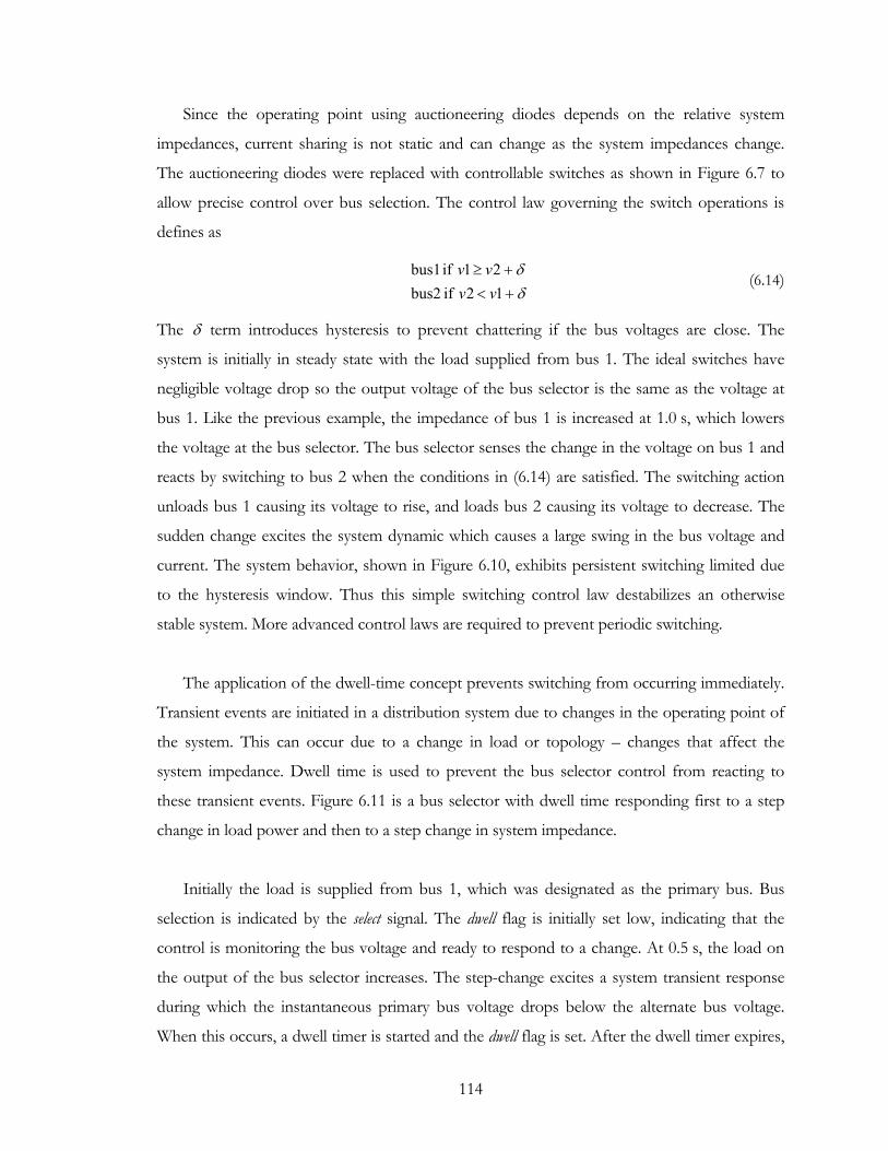
114
Since the operating point using auctioneering diodes depends on the relative system
impedances, current sharing is not static and can change as the system impedances change.
The auctioneering diodes were replaced with controllable switches as shown in Figure 6.7 to
allow precise control over bus selection. The control law governing the switch operations is
defines as
δδ
+<+≥
12 if bus2 21 if bus1
vvvv (6.14)
The δ term introduces hysteresis to prevent chattering if the bus voltages are close. The
system is initially in steady state with the load supplied from bus 1. The ideal switches have
negligible voltage drop so the output voltage of the bus selector is the same as the voltage at
bus 1. Like the previous example, the impedance of bus 1 is increased at 1.0 s, which lowers
the voltage at the bus selector. The bus selector senses the change in the voltage on bus 1 and
reacts by switching to bus 2 when the conditions in (6.14) are satisfied. The switching action
unloads bus 1 causing its voltage to rise, and loads bus 2 causing its voltage to decrease. The
sudden change excites the system dynamic which causes a large swing in the bus voltage and
current. The system behavior, shown in Figure 6.10, exhibits persistent switching limited due
to the hysteresis window. Thus this simple switching control law destabilizes an otherwise
stable system. More advanced control laws are required to prevent periodic switching.
The application of the dwell-time concept prevents switching from occurring immediately.
Transient events are initiated in a distribution system due to changes in the operating point of
the system. This can occur due to a change in load or topology – changes that affect the
system impedance. Dwell time is used to prevent the bus selector control from reacting to
these transient events. Figure 6.11 is a bus selector with dwell time responding first to a step
change in load power and then to a step change in system impedance.
Initially the load is supplied from bus 1, which was designated as the primary bus. Bus
selection is indicated by the select signal. The dwell flag is initially set low, indicating that the
control is monitoring the bus voltage and ready to respond to a change. At 0.5 s, the load on
the output of the bus selector increases. The step-change excites a system transient response
during which the instantaneous primary bus voltage drops below the alternate bus voltage.
When this occurs, a dwell timer is started and the dwell flag is set. After the dwell timer expires,
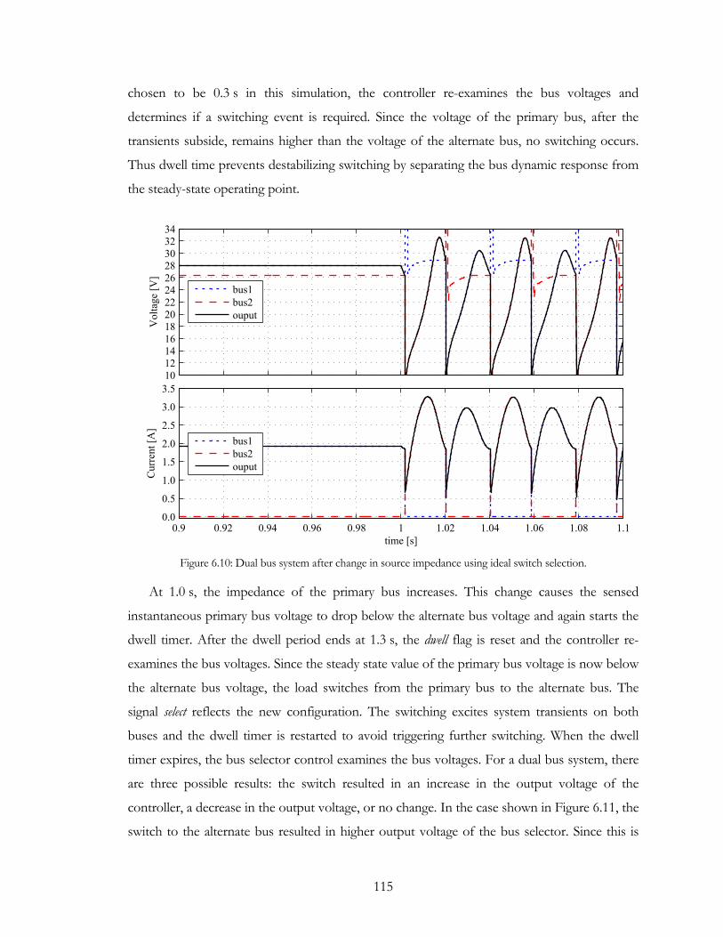
115
chosen to be 0.3 s in this simulation, the controller re-examines the bus voltages and
determines if a switching event is required. Since the voltage of the primary bus, after the
transients subside, remains higher than the voltage of the alternate bus, no switching occurs.
Thus dwell time prevents destabilizing switching by separating the bus dynamic response from
the steady-state operating point.
10121416182022242628303234
Vol
tage
[V]
0.9 0.92 0.94 0.96 0.98 1 1.02 1.04 1.06 1.08 1.10.0
0.5
1.0
1.5
2.0
2.5
3.0
3.5
time [s]
Cur
rent
[A]
bus1bus2ouput
bus1bus2ouput
Figure 6.10: Dual bus system after change in source impedance using ideal switch selection.
At 1.0 s, the impedance of the primary bus increases. This change causes the sensed
instantaneous primary bus voltage to drop below the alternate bus voltage and again starts the
dwell timer. After the dwell period ends at 1.3 s, the dwell flag is reset and the controller re-
examines the bus voltages. Since the steady state value of the primary bus voltage is now below
the alternate bus voltage, the load switches from the primary bus to the alternate bus. The
signal select reflects the new configuration. The switching excites system transients on both
buses and the dwell timer is restarted to avoid triggering further switching. When the dwell
timer expires, the bus selector control examines the bus voltages. For a dual bus system, there
are three possible results: the switch resulted in an increase in the output voltage of the
controller, a decrease in the output voltage, or no change. In the case shown in Figure 6.11, the
switch to the alternate bus resulted in higher output voltage of the bus selector. Since this is
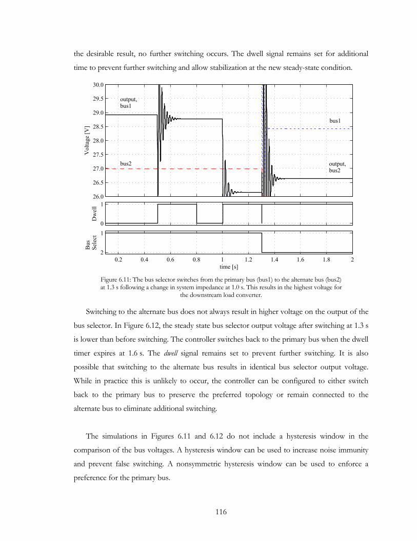
116
the desirable result, no further switching occurs. The dwell signal remains set for additional
time to prevent further switching and allow stabilization at the new steady-state condition.
26.0
26.5
27.0
27.5
28.0
28.5
29.0
29.5
30.0V
olta
ge [V
]
output,bus1
bus2 output,bus2
bus1
0
1
Dw
ell
0.2 0.4 0.6 0.8 1 1.2 1.4 1.6 1.8 22
1
time [s]
Bus
Se
lect
Figure 6.11: The bus selector switches from the primary bus (bus1) to the alternate bus (bus2) at 1.3 s following a change in system impedance at 1.0 s. This results in the highest voltage for
the downstream load converter.
Switching to the alternate bus does not always result in higher voltage on the output of the
bus selector. In Figure 6.12, the steady state bus selector output voltage after switching at 1.3 s
is lower than before switching. The controller switches back to the primary bus when the dwell
timer expires at 1.6 s. The dwell signal remains set to prevent further switching. It is also
possible that switching to the alternate bus results in identical bus selector output voltage.
While in practice this is unlikely to occur, the controller can be configured to either switch
back to the primary bus to preserve the preferred topology or remain connected to the
alternate bus to eliminate additional switching.
The simulations in Figures 6.11 and 6.12 do not include a hysteresis window in the
comparison of the bus voltages. A hysteresis window can be used to increase noise immunity
and prevent false switching. A nonsymmetric hysteresis window can be used to enforce a
preference for the primary bus.
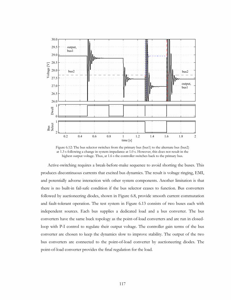
117
26.0
26.5
27.0
27.5
28.0
28.5
29.0
29.5
30.0
Vol
tage
[V]
output,bus1
bus2 bus2
output,bus1
0
1
Dw
ell
0.2 0.4 0.6 0.8 1 1.2 1.4 1.6 1.8 22
1
time [s]
Bus
Se
lect
Figure 6.12: The bus selector switches from the primary bus (bus1) to the alternate bus (bus2) at 1.3 s following a change in system impedance at 1.0 s. However, this does not result in the
highest output voltage. Thus, at 1.6 s the controller switches back to the primary bus.
Active-switching requires a break-before-make sequence to avoid shorting the buses. This
produces discontinuous currents that excited bus dynamics. The result is voltage ringing, EMI,
and potentially adverse interaction with other system components. Another limitation is that
there is no built-in fail-safe condition if the bus selector ceases to function. Bus converters
followed by auctioneering diodes, shown in Figure 6.8, provide smooth current commutation
and fault-tolerant operation. The test system in Figure 6.13 consists of two buses each with
independent sources. Each bus supplies a dedicated load and a bus converter. The bus
converters have the same buck topology as the point-of-load converters and are run in closed-
loop with P-I control to regulate their output voltage. The controller gain terms of the bus
converter are chosen to keep the dynamics slow to improve stability. The output of the two
bus converters are connected to the point-of-load converter by auctioneering diodes. The
point-of-load converter provides the final regulation for the load.
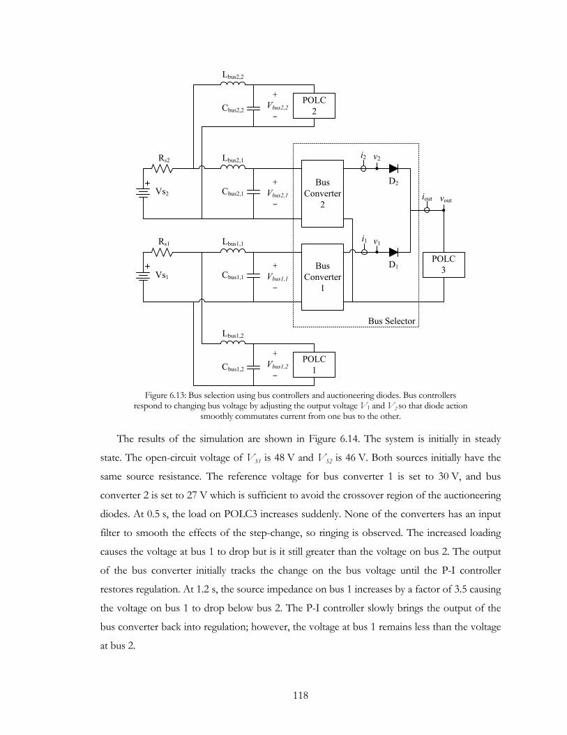
118
v1
v2
POLC3
BusConverter
2vout
Vs2
Rs2 Lbus2,1
Cbus2,1
Vs1
Rs1 Lbus1,1
Cbus1,1
BusConverter
1
D2
D1
Lbus2,2
Cbus2,2POLC
2
Lbus1,2
Cbus1,2POLC
1
iout
i2
i1
+
-Vbus2,2
+
-Vbus2,1
+
-Vbus1,1
+
-Vbus1,2
Bus Selector
Figure 6.13: Bus selection using bus controllers and auctioneering diodes. Bus controllers
respond to changing bus voltage by adjusting the output voltage V1 and V2 so that diode action smoothly commutates current from one bus to the other.
The results of the simulation are shown in Figure 6.14. The system is initially in steady
state. The open-circuit voltage of VS1 is 48 V and VS2 is 46 V. Both sources initially have the
same source resistance. The reference voltage for bus converter 1 is set to 30 V, and bus
converter 2 is set to 27 V which is sufficient to avoid the crossover region of the auctioneering
diodes. At 0.5 s, the load on POLC3 increases suddenly. None of the converters has an input
filter to smooth the effects of the step-change, so ringing is observed. The increased loading
causes the voltage at bus 1 to drop but is it still greater than the voltage on bus 2. The output
of the bus converter initially tracks the change on the bus voltage until the P-I controller
restores regulation. At 1.2 s, the source impedance on bus 1 increases by a factor of 3.5 causing
the voltage on bus 1 to drop below bus 2. The P-I controller slowly brings the output of the
bus converter back into regulation; however, the voltage at bus 1 remains less than the voltage
at bus 2.
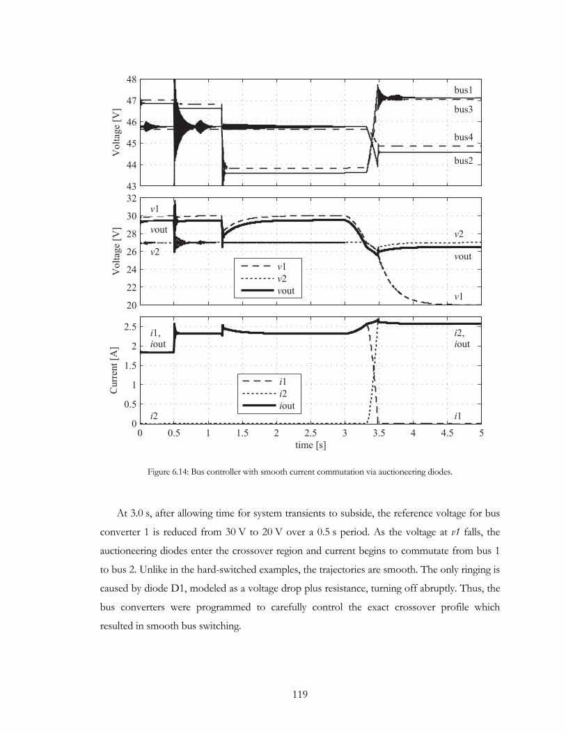
119
43
44
45
46
47
48
Vol
tage
[V]
bus4
bus1
bus2
bus3
20
22
24
26
28
30
32
Vol
tage
[V]
v1
v2
voutv2
vout
v1
0 0.5 1 1.5 2 2.5 3 3.5 4 4.5 50
0.5
1
1.5
2
2.5
time [s]
Cur
rent
[A]
i2, iout
i1
i1, iout
i2
i1i2iout
v1v2vout
Figure 6.14: Bus controller with smooth current commutation via auctioneering diodes.
At 3.0 s, after allowing time for system transients to subside, the reference voltage for bus
converter 1 is reduced from 30 V to 20 V over a 0.5 s period. As the voltage at v1 falls, the
auctioneering diodes enter the crossover region and current begins to commutate from bus 1
to bus 2. Unlike in the hard-switched examples, the trajectories are smooth. The only ringing is
caused by diode D1, modeled as a voltage drop plus resistance, turning off abruptly. Thus, the
bus converters were programmed to carefully control the exact crossover profile which
resulted in smooth bus switching.

120
6.4 Stable Bus Selection with State Dependent Switching
In a multiple bus system where active switching is based on the sensed bus voltages, the
bus selection process is prone to excessive switching due to the dynamics of the system.
Chattering can also occur in a high-impedance system because the bus voltages change as a
function of loading. This section examines active switched bus selection using properties of
hybrid switched systems to develop an analytical justification for using dwell time to ensure
stable switching.
This analysis begins by assuming that each point of load converter has appropriate filtering
so that the input current from the bus is continuous and smooth. The input filter also
decouples the switching dynamics of the converter from the slower dynamics of the input bus.
Therefore the system, viewed from the bus side, exhibits smooth dynamics that evolve
according to the differential algebraic model
( )( )zyxg
zyxfx,,0,,
==&
(6.15)
The function ( )zyxf ,, represents the continuous system dynamics and ( )zyxg ,, provides the
constitutive algebraic equations of the network that determine the bias point of the system.
The variable x is the continuous state variables of inductor currents and capacitor voltages, y
is the auxiliary variables such as source voltages, and z is the binary discrete controls that
represent connections of the load to the N supply buses. The set of possible binary controls is
NΖz 1,0=∈ (6.16)
Dynamic systems that involve the interaction of continuous and discrete dynamics are
referred to as hybrid systems [175]. In the multibus system, switching ideally occurs only as
needed. Thus the problem of interest becomes two continuous-time systems with isolated
discrete switching events. This class of system, known as a switched system [175], can be
derived from the hybrid multibus system by separating the discrete dynamics from the
continuous dynamics in a switched differential algebraic model
( )( )yxg
yxfx
p
p,0
,
=
=& (6.17)

121
Control action to switch among the p source buses introduces state-dependent discrete
switching events indexed by p where
( ) P∈yxp , (6.18)
The index set P is finite and contains the N supply buses from which to select to power the
load
,...N,21=P (6.19)
A second assumption is that all systems of (6.17) in set P are globally stable. This
assumption is satisfied at the interface of the point-of-load converter and input filter by
application of the Middlebrook criterion from (3.13). At the interface to the bus, the
assumption is satisfied by verification of the property of passivity. The linearized system
comprised of the power converter and input filter is written for each supply bus in P :
p
Tpp
ppppp
xCy
uBxAx
=
+=& (6.20)
Passivity is guaranteed for a Hurwitz matrix A and strictly positive real transfer function [175]:
( ) ( ) ppT
pp BAsICsg 1−−= (6.21)
Thus, all possible configurations of the point-of-load converter and supply buses are
independently stable. However, it is well known that unconstrained switching can destabilize a
switched system even if all individual subsystems are stable [175]. In the multibus system, there
are two categories of events that can cause undesirable switching: excited system dynamics and
susceptibility of bus voltage to loading.
6.4.1 System transient response
Events in a power system, such as switching or sudden change in load or generation, can
excite system dynamics. In a properly damped, stable system, this dynamic response decays
quickly. Active bus selection is a form of state-dependent switching where sensed bus voltage

122
is used to determine switching. The switch signal σ is chosen to select the bus with the highest
voltage:
P∈⎟⎟⎠
⎞⎜⎜⎝
⎛= pVp
p,maxargσ (6.22)
If the instantaneous bus voltages are evaluated in (6.22), the dynamics of the system
response, shown at 0.5 s in Figures 6.11 and 6.12, can potentially trigger switching even though
the steady-state values would not. Dwell time is a constrained switching technique that allows
the transient effects to dissipate prior to applying the control law (6.14). If all subsystems are
stable and the dwell time is sufficiently large, stability of the switched system is guaranteed
[175].
Consider a candidate Lyapunov function that represents the magnitude of the transient
ripple voltage on the p system buses:
( ) ripplepp Vt ,≈ (6.23)
Damping in the system provides the exponentially decaying characteristic to the system
response, shown in Figure 6.15. Thus, for the normalized transient response the Lyapunov
function in (6.23) can be approximated by an exponential function:
( ) ( )tp
pet α−= (6.24)
where pα is related to the system damping of the pth bus. The Lyapunov function physically
represents the envelope of the normalized transient response. An example is shown in Figure
6.16.
A lower bound on the dwell time is found when the envelope of the transient response
decays to within the hysteresis limits of the switching control law (6.14):
δ≤ripplepV , (6.25)
This condition implies that the Lyapunov function has become sufficiently small as shown in
Figure 6.16:
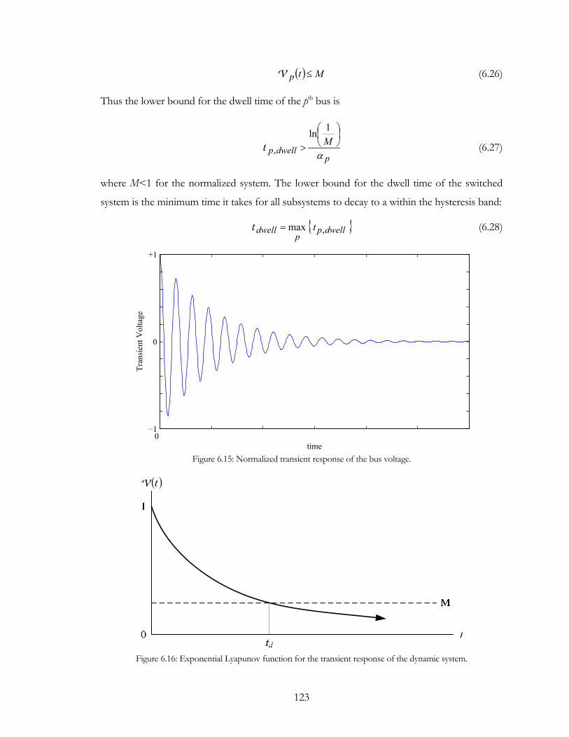
123
( ) Mtp ≤ (6.26)
Thus the lower bound for the dwell time of the pth bus is
p
dwellpM
α
⎟⎠⎞
⎜⎝⎛
>
1ln, (6.27)
where M<1 for the normalized system. The lower bound for the dwell time of the switched
system is the minimum time it takes for all subsystems to decay to a within the hysteresis band:
dwellpp
dwell t ,max= (6.28)
0 −1
0
+1
Tran
sien
t Vol
tage
time Figure 6.15: Normalized transient response of the bus voltage.
( )
Figure 6.16: Exponential Lyapunov function for the transient response of the dynamic system.
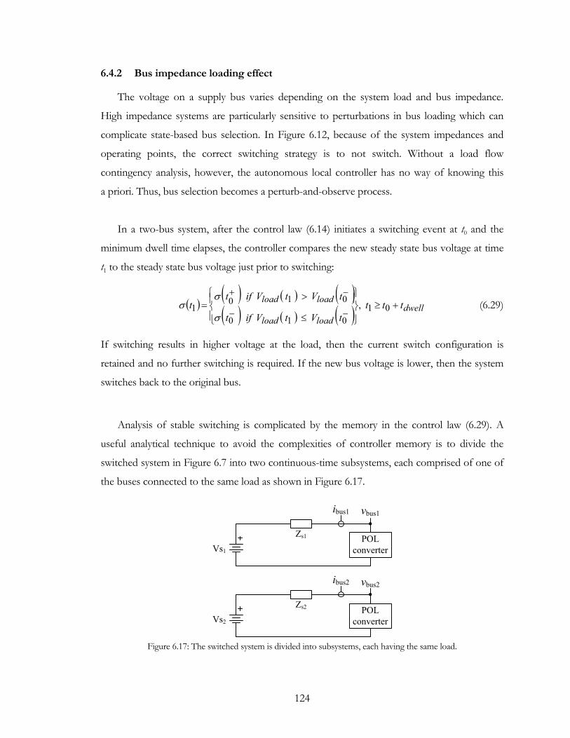
124
6.4.2 Bus impedance loading effect
The voltage on a supply bus varies depending on the system load and bus impedance.
High impedance systems are particularly sensitive to perturbations in bus loading which can
complicate state-based bus selection. In Figure 6.12, because of the system impedances and
operating points, the correct switching strategy is to not switch. Without a load flow
contingency analysis, however, the autonomous local controller has no way of knowing this
a priori. Thus, bus selection becomes a perturb-and-observe process.
In a two-bus system, after the control law (6.14) initiates a switching event at t0 and the
minimum dwell time elapses, the controller compares the new steady state bus voltage at time
t1 to the steady state bus voltage just prior to switching:
( )( ) ( ) ( )( ) ( ) ( ) dwell
loadload
loadload ttttVtVift
tVtViftt +≥
⎪⎭
⎪⎬⎫
⎪⎩
⎪⎨⎧
≤
>=
−−
−+
01010
0101 ,
σ
σσ (6.29)
If switching results in higher voltage at the load, then the current switch configuration is
retained and no further switching is required. If the new bus voltage is lower, then the system
switches back to the original bus.
Analysis of stable switching is complicated by the memory in the control law (6.29). A
useful analytical technique to avoid the complexities of controller memory is to divide the
switched system in Figure 6.7 into two continuous-time subsystems, each comprised of one of
the buses connected to the same load as shown in Figure 6.17.
Vs1
Zs1 POLconverter
vbus1ibus1
Vs2
Zs2 POLconverter
vbus2ibus2
Figure 6.17: The switched system is divided into subsystems, each having the same load.
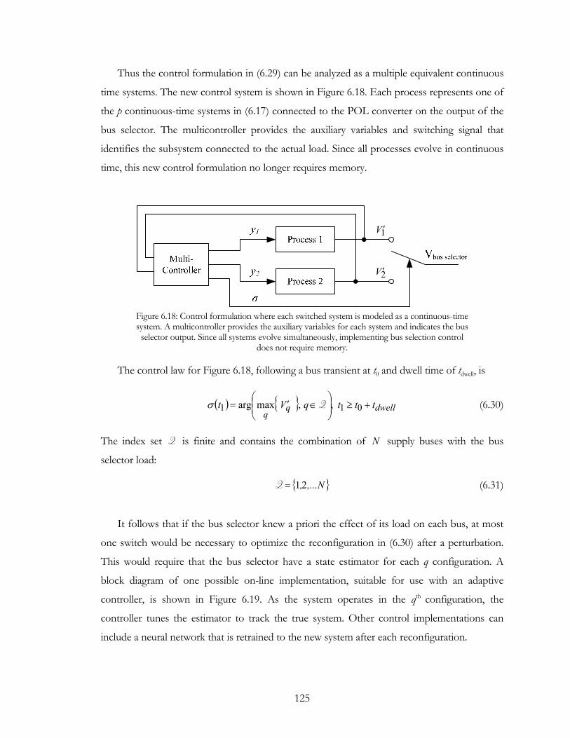
125
Thus the control formulation in (6.29) can be analyzed as a multiple equivalent continuous
time systems. The new control system is shown in Figure 6.18. Each process represents one of
the p continuous-time systems in (6.17) connected to the POL converter on the output of the
bus selector. The multicontroller provides the auxiliary variables and switching signal that
identifies the subsystem connected to the actual load. Since all processes evolve in continuous
time, this new control formulation no longer requires memory.
1V ′
2V ′
Figure 6.18: Control formulation where each switched system is modeled as a continuous-time system. A multicontroller provides the auxiliary variables for each system and indicates the bus
selector output. Since all systems evolve simultaneously, implementing bus selection control does not require memory.
The control law for Figure 6.18, following a bus transient at t0 and dwell time of tdwell, is
( ) dwellqq
tttqVt +≥⎟⎟⎠
⎞⎜⎜⎝
⎛∈′= 011 ,,maxarg Qσ (6.30)
The index set Q is finite and contains the combination of N supply buses with the bus
selector load:
,...N,21=Q (6.31)
It follows that if the bus selector knew a priori the effect of its load on each bus, at most
one switch would be necessary to optimize the reconfiguration in (6.30) after a perturbation.
This would require that the bus selector have a state estimator for each q configuration. A
block diagram of one possible on-line implementation, suitable for use with an adaptive
controller, is shown in Figure 6.19. As the system operates in the qth configuration, the
controller tunes the estimator to track the true system. Other control implementations can
include a neural network that is retrained to the new system after each reconfiguration.
126
Without knowledge of the performance of each subsystem, however, the bus selector is
forced to switch and evaluate. For the dual bus system this translates into at least one switch
shown in Figure 6.11 and at most two switches shown in Figure 6.12. Thus stable bus
switching requires that the maximum number of switches switching is constrained after a
system perturbation.
Figure 6.19: State estimator to implement single switch reconfiguration in a multibus system.
6.5 Conclusions
This chapter examined methods for connecting a point-of-load converter to multiple
supply buses. It was shown that diode OR’ing, a commonly used method, provides smooth
crossover from one bus to another but present an ill-defined operating state when the bus
voltages are similar. Two alternative methods are presented. In the first, controlled switches
replace the diodes and allow carefully orchestrated bus switching. Dwell time, a concept from
hybrid switched-system theory, is used to prevent chattering and ensure stable switching.
This active switching introduces discontinuous current onto the buses that may be
undesirable for critical applications where interference or electromagnetic signature is a
concern. A second solution is proposed that uses auctioneering diodes combined with bus
converters. The diodes ensure continuous current and fail-safe operation and the bus
converter programs the exact profile for bus switching.

127
CHAPTER 7 CONCLUSIONS
Direct current power systems are useful where reliability is of utmost importance.
Traditional applications of dc systems include telephony and spacecraft. Newer applications
include naval shipboard systems, industrial parks, and alternative energy distributed generation
systems. Direct current has even been proposed as a distribution system in future office and
residential buildings. In addition to improved reliability, these newer applications benefit from
greater integration and management of total system resources. Demand-side management, a
paradigm where the load is considered to be an integral partner in system operation and
stability, is important for energy constrained systems such as shipboard power. Traditional
applications can be made more reliable, particularly under emergency conditions, if loads can
be managed to ensure that available energy is allocated for the most critical loads such as life
support and egress systems in buildings.
Fault-tolerant power architectures and control systems prevent faults or failures in a
subsystem component from propagating to the entire system. This dissertation proposed a
demonstration dc system that used dual buses and multiple supplies for redundancy. The focus
for reliability, however, was on the controls. Autonomous locals reside and operate at each
component in the system. They use information obtained locally, from the bus voltage, to
modify the behavior of the component to meet an objective. These controls operate
autonomously and do not rely on communication with a central controller or other peers.
On the supply side, active droop control has been used before for current sharing in
paralleled sources. Droop control was shown to add adjustable damping to the system. In both
applications, whether due to partial loss of generation or the need for more damping, the bus
voltage drops. On the load-side, point-of-load controllers sense this change in the bus voltage
and can infer the health of the system. While they do not know why or how the bus voltage
dropped, they can take steps locally to avert further deterioration. A load-side control strategy
was proposed that integrates a power buffer, dynamic load interruption, and bus selection

128
based on the priority of the load, which provides a structured approach to the decision and
control process.
Details of operation for dynamic load interruption with automatic load restoration and bus
selection were presented. Since these controls use state-dependent switching, chattering is a
concern. Hysteresis and dwell time were used to ensure stable switching. Load interruption
requires voltage set points. In the demonstration system, these were found using a search
algorithm and exhaustive power flow. A general method, suitable for extension to an arbitrary
system, was framed as a bilevel program. For bus selection, principles from hybrid systems
were applied to analyze the system and ensure stable switching.
In conclusion, this dissertation examines a fault-tolerant distributed dc system. Source-side
and load-side techniques were presented that use the system voltage to convey information
about the overall health of the system. Since these controls operate autonomously using locally
obtained information, they enhance the reliability of the power system.
7.1 Future Work
Since this work represented an early effort in this area, the emphasis was on developing the
overall methodology and techniques. The results presented here are encouraging and suggest
that continued work in the area is appropriate. In particular, additional theoretical work is
needed to explore these techniques in larger systems. The issue of existence and uniqueness of
the solution to the bilevel programming problem is paramount to the applicability of these
techniques. In addition, Chapter 5 outlined a method to obtain load-interruption parameters
on-line by monitoring interface impedance. Further work in this area can provide a way for the
autonomous controls to adapt more easily to a changing system, without needing a power flow
program or system-level optimization.
The techniques developed in this dissertation are more broadly applicable beyond the
naval power system. In particular, commercial buildings can benefit from the priority-based
local control for emergency operation. In a disaster scenario, when the building requires
evacuation, critical loads such as emergency lighting and life support systems need preferential
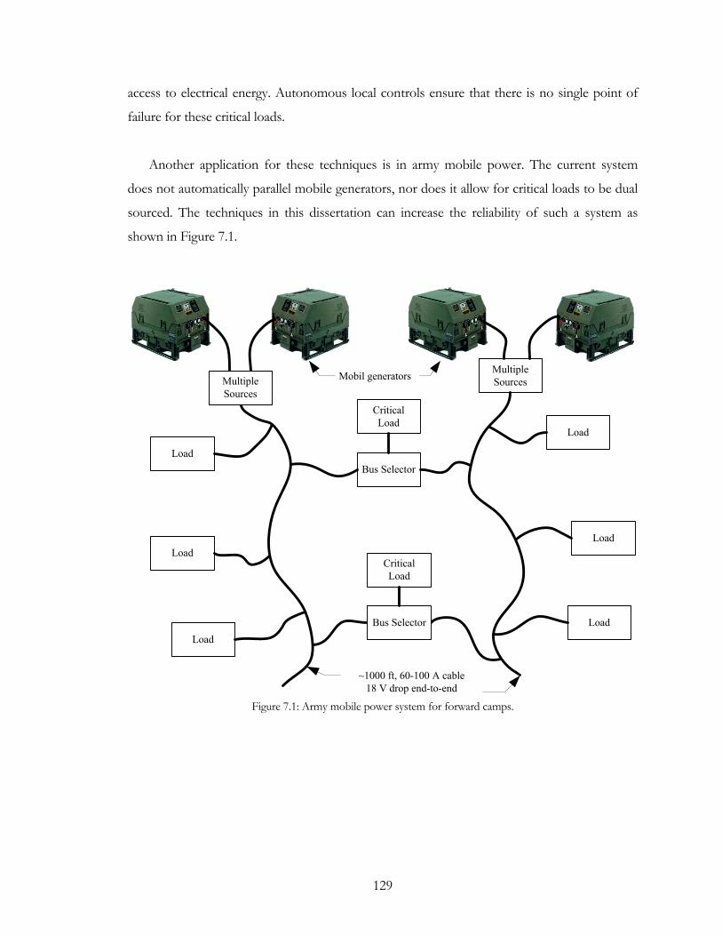
129
access to electrical energy. Autonomous local controls ensure that there is no single point of
failure for these critical loads.
Another application for these techniques is in army mobile power. The current system
does not automatically parallel mobile generators, nor does it allow for critical loads to be dual
sourced. The techniques in this dissertation can increase the reliability of such a system as
shown in Figure 7.1.
MultipleSources
Bus SelectorLoad
Load
Load
CriticalLoad
Bus Selector
CriticalLoad
Load
Load
Load
~1000 ft, 60-100 A cable18 V drop end-to-end
Multiple Sources
Mobil generators
Figure 7.1: Army mobile power system for forward camps.

130
REFERENCES
[1] T. M. Gruzs and J. Hall, "AC, DC or hybrid power solutions for today's telecommunications facilities," in Proceedings, IEEE International Telecommunications Energy Conference (INTELEC), 2000, pp. 361-368.
[2] M. M. Jovanovic, "Dual AC-input power system architectures," in Proceedings, IEEE Applied Power Electronics Conference (APEC), vol. 1, 2002, pp. 584-589.
[3] K. Mistry et al., "Telecommunications power architectures: distributed or centralized," in Proceedings, IEEE International Telecommunications Energy Conference (INTELEC), vol. 1, 1989, p. 10.1.
[4] S. Roy, "Reliability considerations for data centers power architectures," in Proceedings, IEEE International Telecommunications Energy Conference (INTELEC), 2001, pp. 406-411.
[5] "A future naval capability: electric warships & combat vehicles," Office of Naval Research, 2004, http://www.onr.navy.mil/fncs/.
[6] D. H. Clayton, S. D. Sudhoff, and G. F. Grater, "Electric ship drive and power system," in Record, IEEE International Power Modulator Symposium, 2000, pp. 85-88.
[7] H. Hegner and B. Desai, "Integrated fight through power," in Proceedings, IEEE Power Engineering Society Summer Meeting, vol. 1, 2002, pp. 336-339.
[8] E. L. Zivi, "Integrated shipboard power and automation control challenge problem," in Proceedings, IEEE Power Engineering Society Transmission and Distribution Conference, vol. 1, 2002, pp. 325-330.
[9] J. G. Ciezki and R. W. Ashton, "Selection and stability issues associated with a navy shipboard DC zonal electric distribution system," IEEE Transactions on Power Delivery, vol. 15, no. 2, pp. 665-669, Apr. 2000.
[10] B. K. Johnson and R. Lasseter, "An industrial power distribution system featuring UPS properties," in Record, IEEE Power Electronics Specialists Conference (PESC), 1993, pp. 759-765.
[11] W. Tang and R. H. Lasseter, "An LVDC industrial power distribution system without central control unit," in Record, IEEE Power Electronics Specialists Conference, vol. 2, 2000, pp. 979-984.
[12] P. Karlsson, "DC distributed power systems - analysis, design, and control for a renewable energy system," Ph.D. dissertation, Industrial Electrical Engineering, Lund University, 2002.

131
[13] Y. Hu, J. Tatler, and Z. Chen, "A bidirectional DC/DC power electronic converter for an energy storage device in an autonomous power system," in Proceedings, International Power Electronics and Motion Control Conference, vol. 1, 2004, pp. 171-176.
[14] K. Schneider et al., "Real-time control and protection of the NEPTUNE power system," in Oceans Conference Record (IEEE), Institute of Electrical and Electronics Engineers Inc., vol. 3, 2002, pp. 1800-1806.
[15] F. Arteche et al., "EMI filter design and stability assessment of DC voltage distribution based on switching converters," in 7th Workshop on Electronics for LHC Experiments (LEB 2001), 2001, pp. 353-357.
[16] J. A. Weimer, "Electrical power technology for the more electric aircraft," in Proceedings, IEEE/AIAA Digital Avionics Systems Conference, 1993, pp. 445-450.
[17] W. G. Homeyer et al., "Advanced power converters for more electric aircraft applications," in Proceedings, IEEE Intersociety Energy Conversion Engineering Conference, vol. 1, 1996, pp. 137-142.
[18] M. A. Maldonado et al., "Power management and distribution system for a more-electric aircraft (MADMEL): Program status," IEEE Aerospace and Electronic Systems Magazine, vol. 14, no. 12, pp. 3-8, Dec. 1999.
[19] K. P. Louganski, "Modeling and analysis of a DC power distribution system in 21st century airlifters," M.S. thesis, Electrical and Computer Engineering, Virginia Polytechnic Institute and State University, 1999.
[20] E. B. Gietl et al., "The architecture of the electric power system of the International Space Station and its application as a platform for power technology development," in Proceedings, IEEE Energy Conversion Engineering Conference (IECEC), vol. 2, 2000, pp. 855-864.
[21] E. B. Gietl et al., "The electric power system of the International Space Station-a platform for power technology development," in Proceedings, IEEE Aerospace Conference, vol. 4, 2000, pp. 47-54.
[22] A. Emadi, J. P. Johnson, and M. Ehsani, "Stability analysis of large DC solid-state power systems for space," IEEE Aerospace and Electronic Systems Magazine, vol. 15, no. 2, pp. 25-30, 2000.
[23] M. E. Baran and N. R. Mahajan, "DC distribution for industrial systems: Opportunities and challenges," IEEE Transactions on Industry Applications, vol. 39, no. 6, pp. 1596-1601, Nov.-Dec. 2003.
[24] J. Buckley, "Future trends in commercial and military shipboard power systems," in Proceedings, Institute of Electrical and Electronics Engineers Inc. Power Engineering Society Transmission and Distribution Conference, vol. 1, 2002, pp. 340-342.
132
[25] K. Yeager and K. Stahlkoph, "Power for a digital society," in Proceedings, US Department of Energy E-Vision Conference, 2000.
[26] U. Carlsson et al., "Powering the internet - broadband equipment in all facilities - the need for a 300 V DC powering and universal current option," in Proceedings, Institute of Electrical and Electronics Engineers Inc. International Telecommunications Energy Conference (INTELEC), 2003, pp. 164-169.
[27] M. Grossoni et al., "Internet data centres (IDC): Design considerations for mission critical power system performance," in Proceedings, IEEE International Telecommunications Energy Conference (INTELEC), 2001, pp. 353-360.
[28] US Navy ONR/NSF EPNES, "ONR control challenge problem," (white paper), Jan. 19, 2002, http://www.usna.edu/EPNES.
[29] E. L. Zivi and T. J. McCoy, "Control of a shipboard propulsion integrated power system," presented at The 33rd Annual Conference on Information Sciences and Systems (CISS), March 17-19, 1999.
[30] S. Pekarek et al., "Development of a testbed for design and evaluation of power electronic based systems," in Proceedings, Society of Automotive Engineers Power Systems Conference, 2002.
[31] S. D. Pekarek et al., "Overview of a naval combat survivability program," Naval Engineering and Research Consortium (NERC) - Electric Ship Research and Development Consortium (ESRDC), 2004, http://nerc.aticorp.org.
[32] S. D. Sudhoff et al., "Naval combat survivability testbeds for investigation of issues in shipboard power electronics based power and propulsion systems," in IEEE Power Engineering Society Summer Meeting, vol. 1, 2002, pp. 347-350.
[33] G. C. Hua et al., "Development of a DC distributed power system," in Proceedings, IEEE Applied Power Electronics Conference (APEC), 1994, pp. 763-769.
[34] G. S. Thandi et al., "Modeling, control and stability analysis of a PEBB based DC DPS," IEEE Transactions on Power Delivery, vol. 14, no. 2, pp. 497-505, Apr 1999.
[35] W. A. Tabisz, M. M. Jovanovic, and F. C. Lee, "Present and future of distributed power systems," in Proceedings, IEEE Applied Power Electronics Conference (APEC), 1992, pp. 11-18.
[36] S. D. Sudhoff et al., "Stability analysis methodologies for DC power distribution systems," Naval Engineering and Research Consortium (NERC), 2004, http://nerc.aticorp.org/papers/stability.pdf.
[37] S. Glover and S. Sudhoff, "An experimentally validated nonlinear stabilizing control for power electronics-based power systems," in Proceedings, Society of Automotive Engineers Power Systems Conference, 1998.
133
[38] S. Sudhoff and S. Glover, "Modeling techniques, stability analysis, and design criteria for dc power systems with experimental verification," in Proceedings, Society of Automotive Engineers Power Systems Conference, 1998.
[39] S. D. Sudhoff and S. F. Glover, "Three-dimensional stability analysis of dc power electronics based systems," in Record, IEEE Power Electronics Specialist Conference (PESC), vol. 1, 2000, pp. 101-106.
[40] S. D. Sudhoff et al., "Admittance space stability analysis of power electronic systems," IEEE Transactions on Aerospace and Electronic Systems, vol. 36, no. 3 I, pp. 965-973, 2000.
[41] B. M. Howe, H. Kirkham, and V. Vorperian, "Power system considerations for undersea observatories," IEEE Journal of Oceanic Engineering, vol. 27, no. 2, pp. 267-274, April, 2002.
[42] D. W. Harris and F. K. Duennebier, "Powering cabled ocean-bottom observatories," IEEE Journal of Oceanic Engineering, vol. 27, no. 2, pp. 202-211, April 2002.
[43] F. K. Duennebier et al., "HUGO: the Hawaii Undersea Geo-Observatory," IEEE Journal of Oceanic Engineering, vol. 27, no. 2, pp. 218-227, April 2002.
[44] Y. H. Lim and D. C. Hamill, "Nonlinear phenomena in a model spacecraft power system," in Record, IEEE Workshop on Computer in Power Electronics (COMPEL), 1998, pp. 169-175.
[45] E. W. Gholdston et al., "Stability of large DC power systems using switching converters, with application to the International Space Station," in Proceedings, IEEE Energy Conversion Engineering Conference (IECEC), vol. 1, 1996, pp. 166-171.
[46] S. R. Turnquist, M. Twombly, and D. Hoffman, "Space station Freedom power: A reliability, availability, and maintainability assessment of the proposed Space Station Freedom electric power system," in Proceedings, IEEE Intersociety Energy Conversion Engineering Conference, vol. 1, 1989, pp. 271-276.
[47] H. M. Yousef, "Power system management and distribution for future spacecraft," in Digest, IEEE Aerospace Applications Conference, 1991, pp. 4/1-4/10.
[48] J. H. Ly and C. Truong, "Stability analysis of the International Space Station electrical power system," in Proceedings, IEEE International Conference on Control Applications, vol. 1, 1999, pp. 628-633.
[49] I. Lazbin, "Analysis of the stability margins of the space station freedom electric power system," in Record, IEEE Power Electronics Specialist Conference (PESC), 1993, pp. 839-845.
[50] R. C. Lebron, "Load converter interactions with the secondary system in the Space Station Freedom power management and distribution DC test bed," in Proceedings, IEEE Intersociety Energy Conversion Engineering Conference, vol. 6, 1992, pp. 87-92.

134
[51] Y. H. Lim and D. C. Hamill, "Prospects for the application of nonlinear dynamics to spacecraft power systems," in Proceedings of the Fifth European Space Power Conference (ESPC), ESA, vol. 1, 1998, pp. 265-270.
[52] G. M. Masters, Renewable and Efficient Electric Power Systems. Hoboken, NJ: John Wiley & Sons, 2004.
[53] F. Blaabjerg, C. Zhe, and S. B. Kjaer, "Power electronics as efficient interface in dispersed power generation systems," IEEE Transactions on Power Electronics, vol. 19, no. 5, pp. 1184-1194, Sept. 2004.
[54] B. Lasseter, "Microgrids [distributed power generation]," in IEEE Power Engineering Society Winter Meeting, vol. 1, 2001, pp. 146-149.
[55] J. L. Weaver, "Can energy markets be trusted? The effect of the rise and fall of Enron on energy markets," Houston Business and Tax Law Journal, vol. 4, 2004.
[56] K. E. Yeager, "Electricity for the 21st century: Digital electricity for a digital economy," Technology in Society, vol. 26, no. 2-3, pp. 209-221, April/Aug. 2004.
[57] "Electricity technology roadmap - meeting the critical challenges of the 21st century: 2003 summary and synthesis," Electric Power Research Institute (EPRI), Report # 1010929, 2003.
[58] S. Silberman, "The energy web," Wired, no. 9.07, July 2001.
[59] J. Blum, "Bandaged grid still vulnerable: 2003 blackout shed light on weaknesses, but power system fixes fall short of need," Washington Post, Aug. 10, 2004, p. E01.
[60] P. Behr, "Powerless; lights out? The region's fraying electric supply," The Washington Post, sec. Outlook, p. B05.
[61] P. Fairley, "The unruly power grid," IEEE Spectrum, vol. 41, no. 8, pp. 16-21, Aug 2004.
[62] J. Apt et al., "Electrical blackouts: A systemic problem," Issues in Science and Technology, vol. 20, no. 4, pp. 55-61, Summer 2004.
[63] G. B. Sheblé, "Disputing deregulation: Is industrial disorganization on the rise?" IEEE Power and Energy Magazine, vol. 4, no. 1, pp. 16-22, Jan./Feb. 2006.
[64] A. M. Gole et al., "Guidelines for modeling power electronics in electric power engineering applications," IEEE Transactions on Power Delivery, vol. 12, no. 1, pp. 505-514, Jan. 1997.
[65] J. R. Wells et al., "Low-cost single-phase powered induction machine drive for residential applications," in Proceedings, IEEE Applied Power Electronics Conference and Exposition, vol. 3, 2004, pp. 1579-1583.

135
[66] J. Malinowski, "Energy-efficient motors and drives," ASHRAE Journal, vol. 46, no. 1, pp. 30-32, Jan 2004.
[67] M. S. Shur and A. Zukauskas, "Solid-state lighting: toward superior illumination," Proceedings of the IEEE, vol. 93, no. 10, pp. 1691-1703, Oct. 2005.
[68] M. H. J. Bollen, "Voltage sags: effects, mitigation and prediction," Power Engineering Journal, vol. 10, no. 3, pp. 129-135, Jun 1996.
[69] J. Douglas, "Power for a digital society," EPRI Journal, vol. 25, no. 4, pp. 18-25, Winter 2000.
[70] M. Fontela et al., "On the use of distributed generation to increase EPS robustness," in IEEE Power Engineering Society General Meeting, vol. 3, 2005, pp. 2991-2998.
[71] R. Walawalkar and V. Iyer, "Distributed generation for power quality and reliability," in Proceedings, Oklahoma State University Frontiers of Power Conference, 2003, pp. 1-7.
[72] N. D. Hatziargyriou and A. P. S. Meliopoulos, "Distributed energy sources: Technical challenges," in Proceedings, IEEE Power Engineering Society Transmission and Distribution Conference, vol. 2, 2002, pp. 1017-1022.
[73] R. C. Dugan, "Distributed resources and reliability of distribution systems," in Proceedings, IEEE Power Engineering Society Transmission and Distribution Conference, vol. 1, 2002, pp. 106-108.
[74] D. Nilsson and A. Sannino, "Load modelling for steady-state and transient analysis of low-voltage dc systems," in Record, IEEE Industry Applications Conference, vol. 2, 2004, pp. 774-780.
[75] T. E. McDermott and R. C. Dugan, "Distributed generation impact on reliability and power quality indices," in IEEE Rural Electric Power Conference, 2002, pp. D3-1-7.
[76] R. H. Lasseter and P. Paigi, "Microgrid: A conceptual solution," in Record, IEEE Power Electronics Specialists Conference (PESC), vol. 6, 2004, pp. 4285-4290.
[77] T. Blalock, "Powering the New Yorker: A hotel's unique direct current (dc) system," IEEE Power and Energy Magazine, vol. 4, no. 1, pp. 70-75, Jan./Feb. 2006.
[78] A. B. Morton and I. M. Y. Mareels, "The prospects for DC power distribution in buildings," Institution of Engineers (Australia), Journal of Electrical and Electronics Engineering, vol. 20, no. 1, pp. 49-55, 2000.
[79] P. Vaessen, "Direct-current voltage (DC) in households," Leonardo Energy Initiative, 2005, http://digest.copperwire.org/Files/DCHomes.pdf.
[80] A. Sannino, G. Postiglione, and M. H. J. Bollen, "Feasibility of a DC network for commercial facilities," IEEE Transactions on Industry Applications, vol. 39, no. 5, pp. 1499-1507, Sep /Oct 2003.

136
[81] K. Kawamoto et al., "Electricity used by office equipment and network equipment in the US," Energy, vol. 27, no. 3, pp. 255-269, March 2002.
[82] 2004 ASHRAE Handbook: HVAC Systems and Equipment. Atlanta, GA: American Society of Heating Refrigeration and Air-Conditioning Engineers, 2004, p. 46.2-46.3.
[83] W. M. Grady and S. Santoso, "Understanding power system harmonics," IEEE Power Engineering Review, vol. 21, no. 11, pp. 8-11, Nov. 2001.
[84] T. S. Key and J.-S. Lai, "Costs and benefits of harmonic current reduction for switch-mode power supplies in a commercial office building," IEEE Transactions on Industry Applications, vol. 32, no. 5, pp. 1017-1024, Sep.-Oct. 1996.
[85] J.-S. Lai and T. S. Key, "Effectiveness of harmonic mitigation equipment for commercial office buildings," IEEE Transactions on Industry Applications, vol. 33, no. 4, pp. 1104-1110, Jul-Aug 1997.
[86] National Fire Protection Association, National Electric Code, 2002 ed. Batterymarch Park, Quincy: MA: National Fire Protection Association, 2002.
[87] O. Garcia et al., "Power factor correction: A survey," in Record, IEEE Power Electronics Specialists Conference, vol. 1, 2001, pp. 8-13.
[88] O. Garcia et al., "Single phase power factor correction: A survey," IEEE Transactions on Power Electronics, vol. 18, no. 3, pp. 749-755, May 2003.
[89] F. Casamatta et al., "Management of interruptible loads for power system security and operation," in 2002 IEEE Power Engineering Society Summer Meeting, vol. 2, 2002, pp. 880-885.
[90] J. Eto et al., "Innovative developments in load as a reliability resource," in Proceedings, IEEE Power Engineering Society Winter Meeting, vol. 2, 2002, pp. 1002-1004.
[91] S. R. Harper, D. L. Thurston, and P. T. Krein, "The effects of dynamic residential load participation: Penetration levels for operational impact on reliability," International Journal of Critical Infrastructure, submitted for publication.
[92] K. Yeager, S. Gehl, and B. Barker, "The role of smart power technologies in global electrification," Energy and Environment, vol. 16, no. 5, pp. 845-870, 2005.
[93] M. Blanke, "Fault Tolerant Control - an Engineering Approach," Lecture Notes, Department of Control Engineering, Aalborg University, Denmark, 1996.
[94] K. Moslehi et al., "Framework for a self-healing power grid," in Proceedings, IEEE Power Engineering Society General Meeting, vol. 3, 2005, pp. 3027-3034.
[95] M. Amin, "Toward self-healing energy infrastructure systems," IEEE Computer Applications in Power, vol. 14, no. 1, pp. 20-28, Jan 2001.

137
[96] K. Butler-Purry and N. D. R. Sarma, "Preventive self-healing shipboard power distribution systems," in Procedings, IEEE Power Engineering Society General Meeting, vol. 3, 2005, pp. 2443-2444.
[97] Z. Moussaoui et al., "An overview of the control scheme for distributed power systems," in Record, IEEE Southcon/96, 1996, pp. 584-591.
[98] P. Karlsson and J. Svensson, "DC bus voltage control for a distributed power system," IEEE Transactions on Power Electronics, vol. 18, no. 6, pp. 1405-1412, Nov. 2003.
[99] B. K. Johnson et al., "Expandable multiterminal DC systems based on voltage droop," IEEE Transactions on Power Delivery, vol. 8, no. 4, pp. 1926-1932, Oct. 1993.
[100] S. Luo et al., "A classification and evaluation of paralleling methods for power supply modules," in Record, IEEE Power Electronics Specialists Conference (PESC), vol. 2, 1999, pp. 901-908.
[101] T. Van Cutsem and C. Vournas, Voltage Stability of Electric Power Systems. Boston: Kluwer Academic Publishers, 1998, p. xi, 378.
[102] M. Larsson, "Coordinated voltage control in electric power systems," Ph.D. dissertation, Department of Industrial Electrical Engineering, Lund University, 2000.
[103] C. D. Vournas, "Interruptible load as a competitor to local generation for preserving voltage security," in Proceedings, IEEE Power Engineering Society Transmission and Distribution Conference, vol. 1, 2001, pp. 236-240.
[104] O. Samuelsson and B. Eliasson, "Damping of electro-mechanical oscillations in a multimachine system by direct load control," IEEE Transactions on Power Systems, vol. 12, no. 4, pp. 1604-1609, Nov. 1997.
[105] K.-Y. Huang and Y.-C. Huang, "Integrating direct load control with interruptible load management to provide instantaneous reserves for ancillary services," IEEE Transactions on Power Systems, vol. 19, no. 3, pp. 1626-1634, Aug. 2004.
[106] S. Talukdar, C. W. Gellings, and IEEE, Load Management. New York: IEEE Press, 1987.
[107] O. Samuelsson, "Power system damping: Structural aspects of controlling active power," Ph.D. dissertation, Department of Industrial Electrical Engineering and Automation, Lund Institute of Technology, 1997.
[108] "Grid friendly controller helps balance energy supply and demand," Pacific Northwest National Laboratory, 2005, http://gridwise.pnl.gov/docs/pnnlsa36565.pdf.
[109] P. Mazza, "The smart energy network: electricity's third great revolution," Pacific Northwest National Laboratory, Washington, 2003, http://climatesolutions.org/pubs/pdfs/SmartEnergy.pdf.

138
[110] S. Khushalani and N. N. Schulz, "Restoration optimization with distributed generation considering islanding," in Proceedings, IEEE Power Engineering Society General Meeting, vol. 3, 2005, pp. 2445-1449.
[111] C. Moors, D. Lefebvre, and T. Van Cutsem, "Design of load shedding schemes against voltage instability," in Proceedings, IEEE Power Engineering Society Winter Meeting, vol. 2, 2000, pp. 1495-1500.
[112] A. Maiorano et al., "Intelligent load shedding schemes for industrial customers with cogeneration facilities," in Proceedings, IEEE Power Engineering Society Winter Meeting, vol. 2, 1999, pp. 925-930.
[113] M. Woodridge and N. R. Jennings, "Intelligent agents: theory and practice," Knowledge Engineering Review, vol. 10, no. 2, pp. 115-152, 1995.
[114] A. M. Wildberger, "Autonomous adaptive agents for distributed control of the electric power grid in a competitive electric power industry," in Proceedings, IEEE International Conference on Knowledge-Based Intelligent Electronic Systems, vol. 1, 1997, pp. 2-11.
[115] T. Nagata et al., "A multi-agent approach to unit commitment problems," in Proceedings, IEEE Power Engineering Society Transmission and Distribution Conference, vol. 1, 2002, pp. 64-69.
[116] M. Utatani et al., "A multi-agent approach to outage work scheduling for electric power system," in Proceedings, IEEE Power Engineering Society Transmission and Distribution Conference, vol. 3, 2002, pp. 1617-1621.
[117] T. Nagata et al., "A multi-agent approach to power system normal state operations," in Proceedings, IEEE Power Engineering Society Transmission and Distribution Conference, vol. 3, 2002, pp. 1582-1586.
[118] T. Nagata and H. Sasaki, "A multi-agent approach to power system restoration," IEEE Transactions on Power Systems, vol. 17, no. 2, pp. 457-462, May 2002.
[119] L. Li, K. P. Logan, and D. A. Cartes, "Fault detection, diagnostics, and prognostics: Software agent solutions," in IEEE Electric Ship Technologies Symposium, 2005, pp. 425-431.
[120] M. E. Baran and N. Mahajan, "System reconfiguration on shipboard DC zonal electrical system," in IEEE Electric Ship Technologies Symposium, 2005, pp. 86-92.
[121] N. N. Schulz, H. L. Ginn, and S. M. Halpin, "Electric ship research activities and capabilities at Mississippi State University and its partners," in IEEE Electric Ship Technologies Symposium, 2005, pp. 20-27.
[122] A. Emadi and A. Ehsani, "Dynamics and control of multi-converter DC power electronic systems," in Record, IEEE Power Electronics Specialists Conference, vol. 1, 2001, pp. 248-253.

139
[123] N. O. Sokal, "System oscillations caused by negative input resistance at the power input port of a switching mode regulator, amplifier, DC/DC converter, or DC/AC inverter," in Record, IEEE Power Electronics Specialist Conference (PESC), 1973, pp. 138-140.
[124] R. S. Balog, W. W. Weaver, and P. T. Krein, "The load as an energy asset in a distributed architecture," in IEEE Electric Ship Technologies Symposium, 2005, pp. 261-267.
[125] R. S. Balog, W. W. Weaver, and P. T. Krein, "Control strategies to use the load as a dynamic energy asset in a distributed architecture," presented at NSF Electric Power Network Efficiency and Security (EPNES) Workshop, Dec. 4-6, 2005.
[126] R. Erickson and D. Maksimovic, Fundamental of Power Electronics, 2nd ed. Norwell, MA: Kluwer Academic Publishers, 2001.
[127] P. T. Krein, Elements of Power Electronics. New York: Oxford University Press, 1998.
[128] D. M. Mitchell, DC-DC Switching Regulator Analysis. New York: McGraw-Hill, 1988.
[129] B. Andreycak, "Active clamp and reset technique enhances forward converter performance," Texas Instruments, Unitrode Design Seminar SEM1000, slup108, 1994.
[130] D. Dalai, "Design considerations for active clamp and reset technique," Texas Instruments, Unitrode Design Seminar SEM1100, slup112, 1996, http://focus.ti.com/lit/ml/slup112/slup112.pdf.
[131] F. D. Tan, "The forward converter: from the classic to the contemporary," in Proceedings, IEEE Applied Power Electronics Conference (APEC), vol. 2, 2002, pp. 857-863.
[132] Q. M. Li, F. C. Lee, and M. M. Jovanovic, "Large-signal transient analysis of forward converter with active-clamp reset," IEEE Transactions on Power Electronics, vol. 17, no. 1, pp. 15-24, Jan. 2002.
[133] "Power supply topologies," Texas Instruments, Application note sluw001, 2004.
[134] R. D. Middlebrook, "Low-entropy expressions: The key to design-oriented analysis," in IEEE Frontiers in Education Conference, 1991, pp. 399-403.
[135] D. Chen and L. Li, "Novel static inverters with high frequency pulse DC link," IEEE Transactions on Power Electronics, vol. 19, no. 4, pp. 971-978, July 2004.
[136] B. J. Leon and P. A. Wintz, Basic Linear Networks for Electrical and Electronics Engineers. New York: Holt Rinehart and Winston, 1970.
[137] T. Curatolo and S. Cogger, "Enhancing a power supply to ensure EMI compliance," EDN, vol. 50, no. 4, pp. 67-74, Feb. 17, 2005.
[138] D. M. Mitchell, "Power line filter design considerations for DC-DC converters," IEEE Industrial Applications Magazine, vol. 5, no. 6, pp. 16-26, Nov./Dec. 1999.

140
[139] R. D. Middlebrook, "Input filter considerations in design and application of switching regulators," in Record, IEEE Industry Applications Society Annual Meeting, 1976, pp. 366-382.
[140] P. Kundur, N. J. Balu, and M. G. Lauby, Power System Stability and Control. New York: McGraw-Hill, 1994, p. xxiii, 1176.
[141] P. W. Sauer and M. A. Pai, Power System Dynamics and Stability. Upper Saddle River, N.J.: Prentice Hall, 1998, p. x, 357.
[142] C. W. Taylor, D. Maratukulam, and N. J. Balu, Power System Voltage Stability. New York: McGraw-Hill, 1994, p. xiii, 273.
[143] K. T. Vu et al., "Voltage instability: Mechanisms and control strategies," Proceedings of the IEEE, vol. 83, no. 11, pp. 1442-1455, Nov. 1995.
[144] J. W. Nilsson, Electric Circuits, 4th ed. Reading, Mass.: Addison-Wesley Pub. Co., 1993.
[145] P. Zumel et al., "EMI reduction by interleaving of power converters," in Proceedings, IEEE Applied Power Electronics Conference (APEC), vol. 2, 2004, pp. 688-694.
[146] K. Xing et al., "An active bus conditioner for a distributed power system," in Record, IEEE Power Electronics Specialist Conference (PESC), vol. 2, 1999, pp. 895-900.
[147] R. Balog and P. T. Krein, "Automatic tuning of coupled inductor filters," in Record, IEEE Power Electronics Specialists Conference (PESC), vol. 2, 2002, pp. 591-596.
[148] R. S. Balog, "Coupled inductor: A basic filter building block - analysis, simulation, and examples," M.S. thesis, Department of Electrical and Computer Engineering, University of Illinois at Urbana-Champaign, 2002.
[149] J. Phinney and D. J. Perreault, "Filters with active tuning for power applications," IEEE Transactions on Power Electronics, vol. 18, no. 2, pp. 636-647, March 2003.
[150] R. D. Middlebrook, "Null double injection and the extra element theorem," IEEE Transactions on Education, vol. 32, no. 3, pp. 167-180, Aug 1990.
[151] M. Florez-Lizarraga and A. F. Witulski, "Input filter design for multiple-module DC power systems," IEEE Transactions on Power Electronics, vol. 11, no. 3, pp. 472-479, May 1996.
[152] C. M. Wildrick et al., "A method of defining the load impedance specification for a stable distributed power system," IEEE Transactions on Power Electronics, vol. 10, no. 3, pp. 280-285, May 2005.
[153] X. Feng, J. Liu, and F. C. Lee, "Impedance specifications for stable DC distributed power systems," IEEE Transactions on Power Electronics, vol. 17, no. 2, pp. 157-162, Mar 2002.

141
[154] D. L. Logue and P. T. Krein, "Preventing instability in DC distribution systems by using power buffering," in Record, IEEE Power Electronics Specialist Conference, vol. 1, 2001, pp. 33-37.
[155] W. W. Weaver and P. T. Krein, "Mitigation of power system collapse through active dyanamic buffers," in Record, IEEE Power Electronics Specialists Conference, vol. 2, 2004, pp. 1080-1084.
[156] A. von Jouanne, P. N. Enjeti, and B. Banerjee, "Assessment of ride-through alternatives for adjustable-speed drives," IEEE Transactions on Industry Applications, vol. 35, no. 4, pp. 908-916, July-Aug. 1999.
[157] A. Van Zyl et al., "Voltage sag ride-through for adjustable-speed drives with active rectifiers," IEEE Transactions on Industry Applications, vol. 34, no. 6, pp. 1270-1277, Nov.-Dec. 1998.
[158] Y. Akashi, J. Neches, and A. Beierman, "Energy savings for load-shedding ballast for fluorescent lighting systems: Occupant's dimming requirements," Lighting Research Center, Rensselaer Polytechnic Institute, 2002.
[159] Y. Akashi and J. Neches, "Potential recommendations for illuminance reductions by load-shedding," Lighting Research and Technology, vol. 37, no. 2, pp. 133-153, June 2005.
[160] J. A. Momoh, S. S. Kaddah, and W. Salawu, "Security assessment of DC zonal naval-ship power system," in Proceedings, IEEE Large Engineering Systems Conference on Power Engineering, 2001, pp. 206-212.
[161] Z. Ye et al., "Design of parallel sources in DC distributed power systems by using gain-scheduling technique," in Record, IEEE Power Electronics Specialist Conference, vol. 1, 1999, pp. 161-165.
[162] X. Zhou et al., "Investigation of candidate VRM topologies for future microprocessors," IEEE Transactions on Power Electronics, vol. 15, no. 6, pp. 1172-1182, Nov. 2000.
[163] Cherry Tree Scientific Software, Power System Toolbox, ver. 2.0, http://www.eagle.ca/~cherry/pst.htm.
[164] B. Colson, P. Marcotte, and G. Savard, "Bilevel programming: A survey," 4OR: A Quarterly Journal of Operations Research, vol. 3, no. 2, pp. 87-107, June 2005.
[165] L. N. Vicente and P. H. Calamai, "Bilevel and multilevel programming. A bibliography review," Journal of Global Optimization, vol. 5, no. 3, pp. 291-306, Oct. 1994.
[166] J. Salmeron, K. Wood, and R. Baldick, "Analysis of electric grid security under terrorist threat," IEEE Transactions on Power Systems, vol. 19, no. 2, pp. 905-912, May 2004.
[167] J. M. Arroyo and F. D. Galiana, "On the solution of the bilevel programming formulation of the terrorist threat problem," IEEE Transactions on Power Systems, vol. 20, no. 2, pp. 789-797, May 2005.

142
[168] G. Brown, M. Carlyle, and J. Salmeron, "Defending critical infrastructure," Operations Research Department, Naval Postgraduate School, Monterey, Ca, 2005, http://www.nps.navy.mil/orfacpag/resumePages/papers/BrownEtAlCIP05.pdf.
[169] X. Feng and F. C. Lee, "On-line measurement on stability margin of DC distributed power system," in Proceedings, IEEE Applied Power Electronics Conference (APEC), vol. 2, 2000, pp. 1190-1196.
[170] X. Feng et al., "Fault detection in DC distributed power systems based on impedance characteristics of modules," in Record, IEEE Industry Applications Conference, vol. 4, 2000, pp. 2455-2462.
[171] N. D. Benavides and P. L. Chapman, "Power budgeting of a multiple-input buck-boost converter," IEEE Transactions on Power Electronics, vol. 20, no. 6, pp. 1303-1309, Nov. 2005.
[172] B. G. Dobbs and P. L. Chapman, "A multiple-input DC-DC converter topology," IEEE Power Electronics Letters, vol. 1, no. 1, pp. 6-9, Mar. 2003.
[173] D. Liberzon, "Hybrid Systems and Control," University of Illinois at Urbana-Champaign, ECE 497 Class Notes, Fall 2002.
[174] "MUR3020PT Ultrafast Rectifier," Jan. 2002, Rev. 6, On Semiconductor, 2004, www.onsemi.com.
[175] D. Liberzon, Switching in Systems and Control. Boston: Birkhäuser, 2003.

143
APPENDIX A EXPERIMENTAL HARDWARE DETAILS
Extensive custom-designed hardware and firmware were developed for experimental
verification of the control algorithms in this dissertation. It is expected that this design effort
can be leveraged by subsequent investigation. The important design components listed in
Table A.1 have been documented and deposited in the in the UIUC Power Electronics Design
Archives.
Table A.1: UIUC Power Electronics Design Archive part numbers for custom hardware and firmware.
System Part Number Buck dc-dc converter schematic SK0019 Buck dc-dc converter PCB PB0019 POL controller schematic SK0023 POL controller PCB PB0023 Firmware for POL controller SW0027 Heatsink assembly with fan PJ0018
This appendix is organized into sections providing details for the buck converter and POL
controller listed in Table A.1. Section A.1 provides the design details for the buck dc-dc
converter hardware. Section A.2 provides the design details for the point-of-load controller
hardware. Section A.3 contains the listing of the firmware code for the point-of-load
controller.
A.1 Point-of-Load Buck Converter
The design of the buck converter is deliberately simple to allow flexibility. The power stage
uses a high-side MOSFET as the main switch and supports either diode or synchronous
rectification. A high and low side boot-strapped gate drive provides independent control for
the main switch and synchronous rectification, if used. The output filter is designed for board
mounting of two different sized ferrite pot cores. Extra pads are provided for other inductor
form-factors. Multiple pads are provided for ceramic and electrolytic filter capacitors on both
the output and input side. Output load can be connected on-board with pads spaced for 5 W
Ohmite resistors or externally via banana jacks. A MOSFET allows a second on-board or
external load to be switched in parallel with the primary load to support load-step operation.

144
Instrumentation is facilitated via a wire loop to allow a current probe to monitor the inductor
current and test points to monitor important voltages.
The voltage-mode control is implemented in discrete analog circuitry to allow direct
observation or modification to all aspects of the PWM process. Extra op-amps are provided to
support modification to current-mode control. Jumpers select between closed-loop and open-
loop operation. The PWM control signal is modified by a dead-time circuit to provide
complementary signals with dead-time to support synchronous rectification. Test points are
provided for each important control signal.
The buck converter hardware was designed to work with a digital supervisory controller
via a SPI interface. Four successive approximation 12 bit analog-to-digital converters monitor
the input voltage, the output voltage, and the inductor current. The last channel is
uncommitted. A dual channel digital potentiometer is jumper selectable to control the
frequency of the voltage-controlled oscillator that generates the PWM ramp. The second
channel is uncommitted and can be used with the extra op-amps to tune the performance of
the feedback control. Extra digital signals enable the gate drive signal and load-step resistor.
This section provides complete design and performance details for the buck converter.
Figure A.1 shows the silkscreen later for the PCB and Figures A.2 – A.8 contain the
electrical schematic. Figure A.9 show the design details for the custom filter inductor. Figure
A.10 – A.15 provides experimental performance data for the voltage-mode buck converter.
Figure A.16 – A.19 provide the theoretical analysis of the small-signal transfer functions for
the open-loop and closed-loop buck converters.
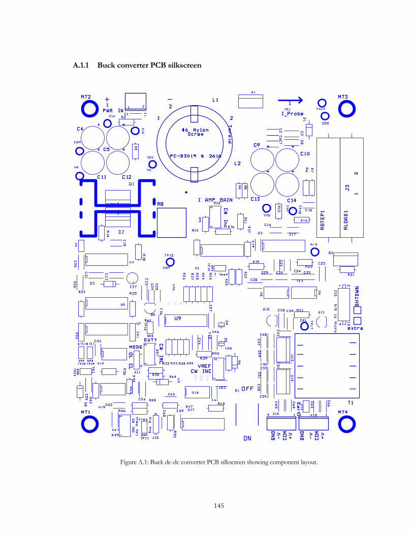
145
A.1.1 Buck converter PCB silkscreen
Figure A.1: Buck dc-dc converter PCB silkscreen showing component layout.
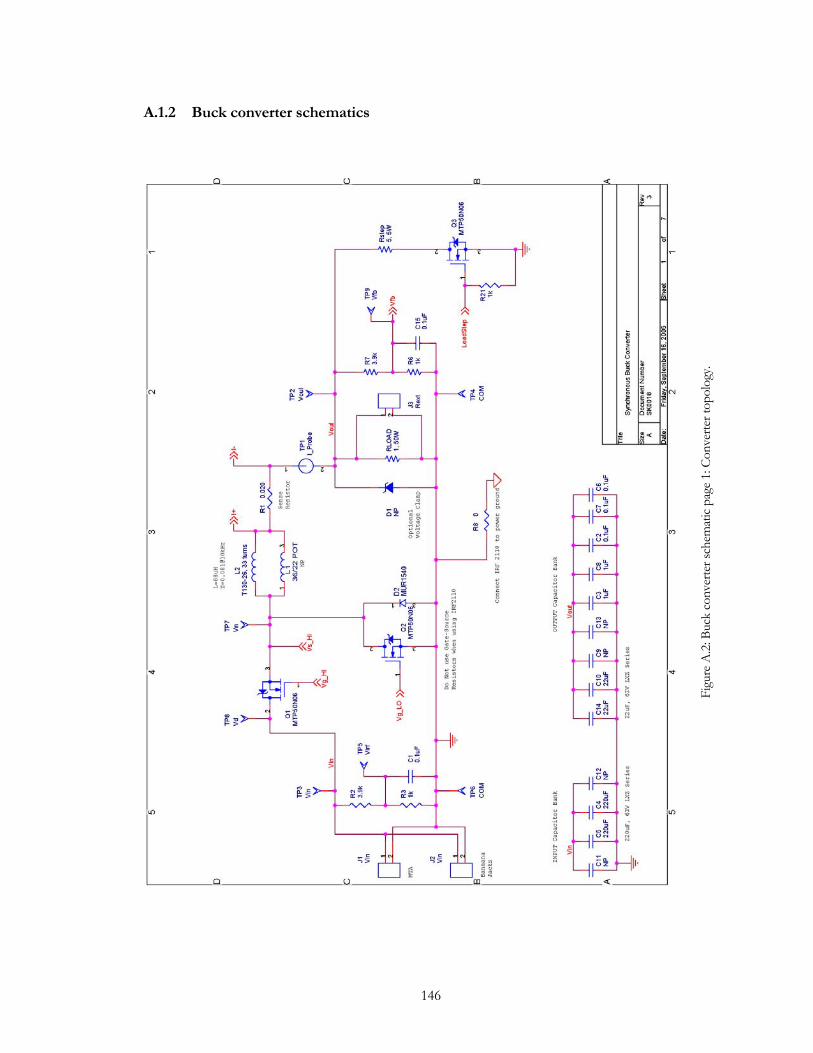
146
A.1.2 Buck converter schematics
Figu
re A
.2: B
uck
conv
erte
r sch
emat
ic pa
ge 1
: Con
verte
r top
olog
y.
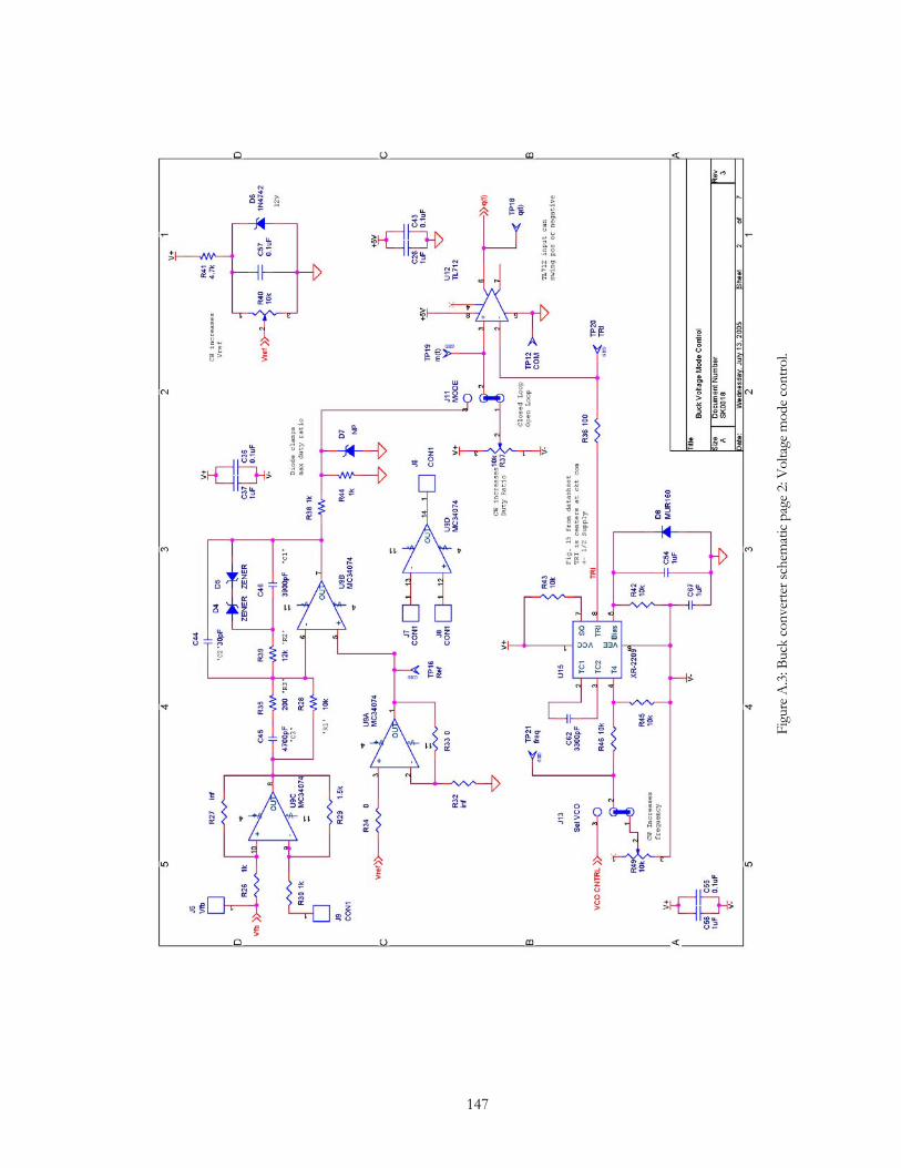
147
Figu
re A
.3: B
uck
conv
erte
r sch
emat
ic pa
ge 2
: Vol
tage
mod
e con
trol.
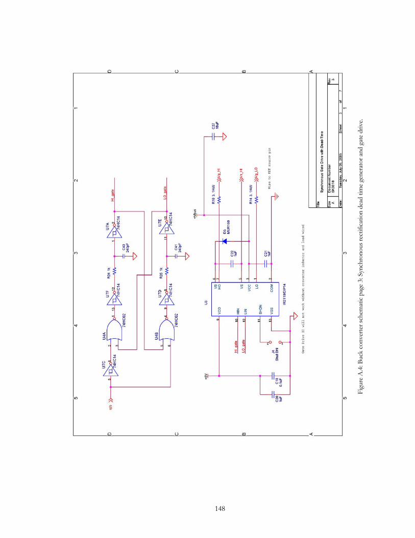
148
Figu
re A
.4: B
uck
conv
erte
r sch
emat
ic pa
ge 3
: Syn
chro
nous
rect
ifica
tion
dead
tim
e gen
erat
or an
d ga
te d
rive.
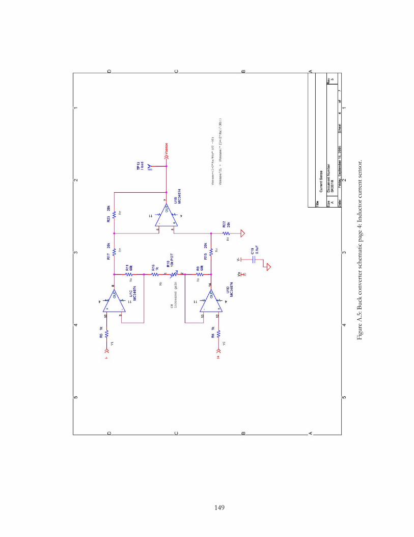
149
Figu
re A
.5: B
uck
conv
erte
r sch
emat
ic pa
ge 4
: Ind
ucto
r cur
rent
sens
or.
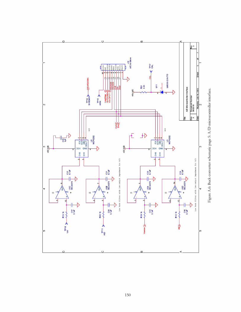
150
Figu
re A
.6: B
uck
conv
erte
r sch
emat
ic pa
ge 5
: A/D
micr
ocon
trolle
r int
erfa
ce.
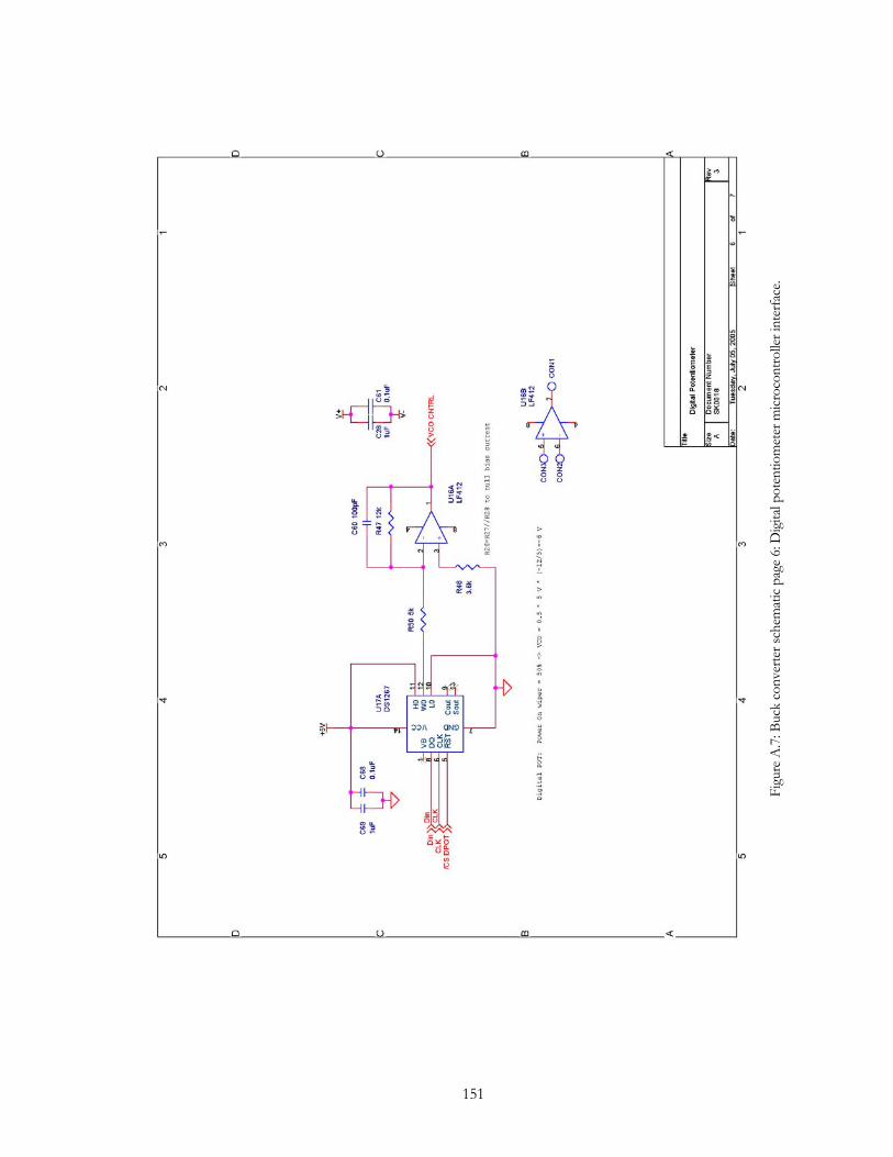
151
Figu
re A
.7: B
uck
conv
erte
r sch
emat
ic pa
ge 6
: Dig
ital p
oten
tiom
eter
micr
ocon
trolle
r int
erfa
ce.
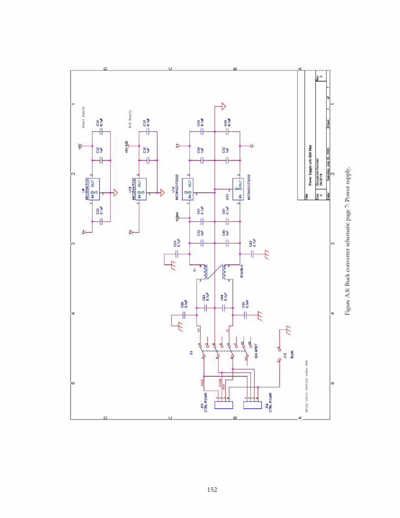
152
Figu
re A
.8: B
uck
conv
erte
r sch
emat
ic pa
ge 7
: Pow
er su
pply.

153
A.1.3 Buck converter filter inductor design
Torroid Inductor designC opyright 2004 by R obert S .Balog, all rights reserved.
Objective: To design a powdered iron toroidal inductor. Design parameters are entered in highlighted regions.
Database parts are all 26 type material powdered iron - yellow with white strip: (Data taken from Micrometals)
Inductor S pecifications:
T130 T200 T200-D T300-D T400-D Other C ore size available
14AW G 16AW G 18AW G 20AW G 22AW G W ire size available
V max 40 V:= Maximum voltage across the inductor
L 88mH:= Desired inductance
f 50kHz:= S witching frequency
D 30%:= Duty ratio
p 1:= Number of parallel wires
Inductor design:C ore parameters:
A L 81 nH= mr 75= OD 1.299 in= Ht 0.437 in=
Number of turns:
N ceilL
A L:=
N 33=
S aturation Limitation:
ImaxBsat A core
A L N:= Imax 7.83 A= Maximum dc current to avoid saturation
NminV max D
Bsat A core f:= Nmin 11.5= Minimum number of turns to avoid ac flux saturation
Maximum energy storage:
W max Bsat2 lcore A core
2 mcore:= W max 2.759 10
3-· J=
Length of wire for each turn:
wirelengthturn 2 Ht 2 OD ID-( )+:= wirelengthturn 3.411 in=
Total length of wire needed (assumes close winding packing):
wirelength N wirelengthturn:= wirelength 112.564 in=
DC S eries R esistances (copper resistance):
P rint All R ecalculateR S
R wire
pwirelength:= R S 37.17 mW=
Figure A.9: Buck converter inductor design.
A.1.4 Buck converter ripple
The prototype converter was built using a MOSFET high-side switch and an ultrafast
rectifier. The efficiency of the buck converter is greatest at high output voltage and low input
voltage as shown in Figure A.10. High output voltage requires a high duty ratio for a given
input voltage show in Figure A.11. Similarly, low input voltage requires a high duty ratio for a
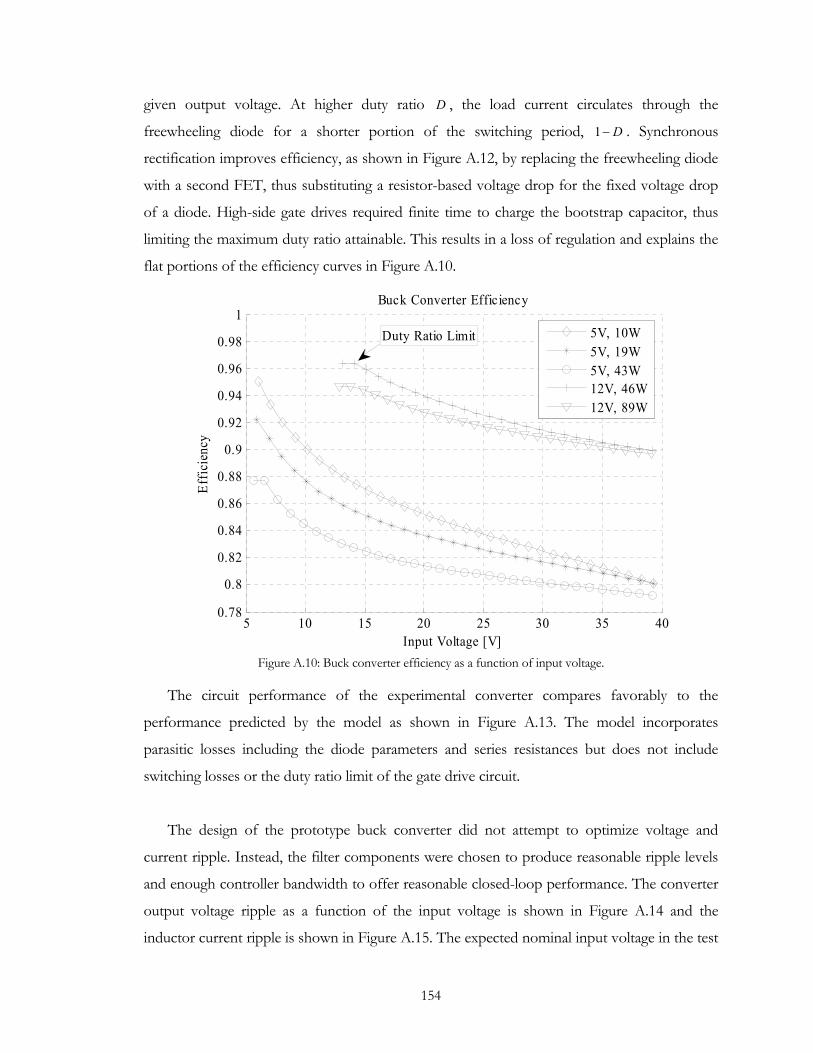
154
given output voltage. At higher duty ratio D , the load current circulates through the
freewheeling diode for a shorter portion of the switching period, D−1 . Synchronous
rectification improves efficiency, as shown in Figure A.12, by replacing the freewheeling diode
with a second FET, thus substituting a resistor-based voltage drop for the fixed voltage drop
of a diode. High-side gate drives required finite time to charge the bootstrap capacitor, thus
limiting the maximum duty ratio attainable. This results in a loss of regulation and explains the
flat portions of the efficiency curves in Figure A.10.
5 10 15 20 25 30 35 400.78
0.8
0.82
0.84
0.86
0.88
0.9
0.92
0.94
0.96
0.98
1
Input Voltage [V]
Effic
ienc
y
Buck Converter Efficiency
5V, 10W5V, 19W5V, 43W12V, 46W12V, 89W
Duty Ratio Limit
Figure A.10: Buck converter efficiency as a function of input voltage.
The circuit performance of the experimental converter compares favorably to the
performance predicted by the model as shown in Figure A.13. The model incorporates
parasitic losses including the diode parameters and series resistances but does not include
switching losses or the duty ratio limit of the gate drive circuit.
The design of the prototype buck converter did not attempt to optimize voltage and
current ripple. Instead, the filter components were chosen to produce reasonable ripple levels
and enough controller bandwidth to offer reasonable closed-loop performance. The converter
output voltage ripple as a function of the input voltage is shown in Figure A.14 and the
inductor current ripple is shown in Figure A.15. The expected nominal input voltage in the test
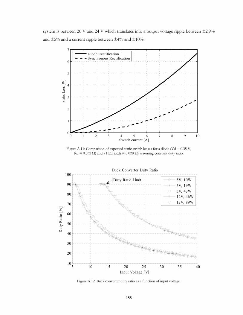
155
system is between 20 V and 24 V which translates into a output voltage ripple between ±2.9%
and ±5% and a current ripple between ±4% and ±10%.
0 1 2 3 4 5 6 7 8 9 100
1
2
3
4
5
6
7
Switch current [A]
Stat
ic L
oss [
W]
Diode RectificationSynchronous Rectification
Figure A.11: Comparison of expected static switch losses for a diode (Vd = 0.35 V,
Rd = 0.032 Ω) and a FET (Rds = 0.028 Ω) assuming constant duty ratio.
Figure A.12: Buck converter duty ratio as a function of input voltage.
5 10 15 20 25 30 35 4010
20
30
40
50
60
70
80
90
100
Input Voltage [V]
Dut
y Ra
tio [%
]
Buck Converter Duty Ratio
5V, 10W5V, 19W5V, 43W12V, 46W12V, 89W
Duty Ratio Limit
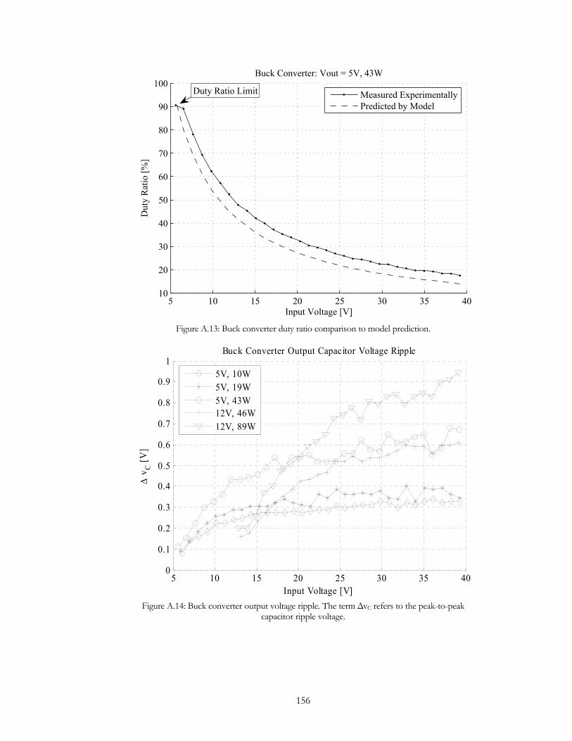
156
5 10 15 20 25 30 35 4010
20
30
40
50
60
70
80
90
100
Input Voltage [V]
Dut
y R
atio
[%]
Buck Converter: Vout = 5V, 43W
Measured ExperimentallyPredicted by Model
Duty Ratio Limit
Figure A.13: Buck converter duty ratio comparison to model prediction.
5 10 15 20 25 30 35 400
0.1
0.2
0.3
0.4
0.5
0.6
0.7
0.8
0.9
1
Input Voltage [V]
∆ v
C [V]
Buck Converter Output Capacitor Voltage Ripple
5V, 10W5V, 19W5V, 43W12V, 46W12V, 89W
Figure A.14: Buck converter output voltage ripple. The term ∆vC refers to the peak-to-peak
capacitor ripple voltage.
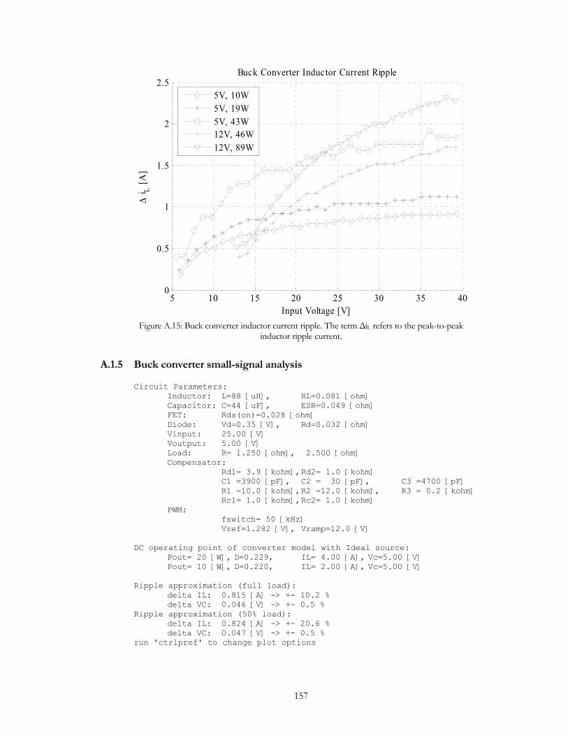
157
5 10 15 20 25 30 35 400
0.5
1
1.5
2
2.5
Input Voltage [V]
∆ i L [A
]
Buck Converter Inductor Current Ripple
5V, 10W5V, 19W5V, 43W12V, 46W12V, 89W
Figure A.15: Buck converter inductor current ripple. The term ∆iL refers to the peak-to-peak
inductor ripple current.
A.1.5 Buck converter small-signal analysis
Circuit Parameters: Inductor: L=88 [uH], RL=0.081 [ohm] Capacitor: C=44 [uF], ESR=0.049 [ohm] FET: Rds(on)=0.028 [ohm] Diode: Vd=0.35 [V], Rd=0.032 [ohm] Vinput: 25.00 [V] Voutput: 5.00 [V] Load: R= 1.250 [ohm], 2.500 [ohm] Compensator: Rd1= 3.9 [kohm], Rd2= 1.0 [kohm] C1 =3900 [pF], C2 = 30 [pF], C3 =4700 [pF] R1 =10.0 [kohm], R2 =12.0 [kohm], R3 = 0.2 [kohm] Rc1= 1.0 [kohm], Rc2= 1.0 [kohm] PWM: fswitch= 50 [kHz] Vref=1.282 [V], Vramp=12.0 [V] DC operating point of converter model with Ideal source: Pout= 20 [W], D=0.229, IL= 4.00 [A], Vc=5.00 [V] Pout= 10 [W], D=0.220, IL= 2.00 [A], Vc=5.00 [V] Ripple approximation (full load): delta IL: 0.815 [A] -> +- 10.2 % delta VC: 0.046 [V] -> +- 0.5 % Ripple approximation (50% load): delta IL: 0.824 [A] -> +- 20.6 % delta VC: 0.047 [V] -> +- 0.5 % run 'ctrlpref' to change plot options

158
Buck Converter control to output Gvd(s): Transfer function: 6.766e-005 s + 31.71 ------------------------------------- 5.028e-009 s^2 + 9.707e-005 s + 1.362
Buck Converter control to output Gvd(s) 50% loaded: Transfer function: 0.0001353 s + 63.41 ------------------------------------ 9.868e-009 s^2 + 0.0001059 s + 2.612 Zero frequencies [kHz]: full load: 74.58 light load: 74.58 Pole frequencies [kHz]: full load: 2.62 2.62 light load: 2.59 2.59 Gain Margin (full load): Gm=Inf dB @ NaN rad/s (NaN kHz) Phase Margin (full load): Pm=23.80 Deg @ 8.05e+004 rad/s (12.81 kHz) DC gain: 27.3392 [db] Rated Load 27.7041 [db] 50% load
The bode plot of the transfer functions above were used to generate Figure A.16.
Buck Converter input to output Gvg(s): Transfer function: 6.101e-007 s + 0.2859 ------------------------------------- 5.028e-009 s^2 + 9.707e-005 s + 1.362 Buck Converter input to output Gvg(s) 50% loaded: Transfer function: 1.22e-006 s + 0.5718 ------------------------------------ 9.868e-009 s^2 + 0.0001059 s + 2.612 Zero frequencies [kHz]: full load: 74.58 light load: 74.58 Pole frequencies [kHz]: full load: 2.62 2.62 light load:

159
2.59 2.59 Gain Margin (full load): Gm=Inf dB @ NaN rad/s (NaN kHz) Phase Margin (full load): Pm=Inf Deg @ NaN rad/s (NaN kHz) DC gain: -13.5594 [db] Rated Load -13.1944 [db] 50% load
The bode plot of the transfer functions above were used to generate Figure A.17.
Buck Converter output impedance Zo(s): Transfer function: -2.347e-010 s^2 - 0.0001103 s - 0.1401 -------------------------------------- 5.028e-009 s^2 + 9.707e-005 s + 1.362 Buck Converter output impedance Zo(s) 50% loaded: Transfer function: -4.695e-010 s^2 - 0.0002206 s - 0.2802 -------------------------------------- 9.868e-009 s^2 + 0.0001059 s + 2.612 Zero frequencies [kHz]: full load: 74.58 0.20 50%t load: 74.58 0.20 Pole frequencies [kHz]: full load: 2.62 2.62 50%t load: 2.59 2.59 Gain Margin (full load): Gm=0.880077 dB @ 1.60e+004 rad/s (2.55 kHz) Phase Margin (full load): Pm=24.07 Deg @ 1.20e+004 rad/s (1.91 kHz) Compensator: H(s) Transfer function: 2.244e-009 s^2 + 9.474e-005 s + 1 -------------------------------------------- 1.32e-017 s^3 + 5.098e-011 s^2 + 3.93e-005 s Zero frequencies [kHz]: 3.40 3.32 Pole frequencies [kHz]: 0.00 445.50 169.31 Gain Margin: Gm=Inf dB @ NaN rad/s (NaN kHz) Phase Margin: Pm=91.29 Deg @ 1.70e+008 rad/s (27051.38 kHz) Feedback divider (sensor) scalar gain: Ho

160
Transfer function: 0.2041 Compensator actuator scalar gain: Ha Transfer function: 0.5 Modulator scalar gain: M Transfer function: 0.08333
The bode plot of the transfer functions above is shown in Figure A.18. Open Loop Gain: T(s)=Ho*H(s)Ha*M*Gvd(S) (at rated load): Transfer function: 1.518e-007 s^3 + 0.07755 s^2 + 3072 s + 3.171e007 ---------------------------------------------------------------------- 7.803e-018 s^5 + 3.029e-011 s^4 + 2.382e-005 s^3 + 0.4568 s^2 + 6295 s Zero frequencies [kHz] (full load): 74.58 3.40 3.32 Pole frequencies [kHz] (full load): 0.00 445.50 169.31 2.62 2.62 Gain Margin (full load): Gm=Inf dB @ Inf rad/s (Inf kHz) Phase Margin (full load): Pm=95.68 Deg @ 5.55e+003 rad/s (0.88 kHz)
The bode plot of the transfer function above is shown in Figure A.19
Open Loop Gain: T(s)=Ho*H(s)Ha*M*Gvd(S) (at 50% load): Transfer function: 3.036e-007 s^3 + 0.1551 s^2 + 6143 s + 6.342e007 --------------------------------------------------------------------------- 1.532e-017 s^5 + 5.933e-011 s^4 + 4.624e-005 s^3 + 0.5051 s^2 + 1.207e004 s Zero frequencies [kHz] (50% load): 74.58 3.40 3.32 Pole frequencies [kHz] (50% load): 0.00 445.50 169.31 2.59 2.59 Gain Margin (50% load): Gm=Inf dB @ Inf rad/s (Inf kHz) Phase Margin (50% load): Pm=107.21 Deg @ 6.55e+003 rad/s (1.04 kHz)
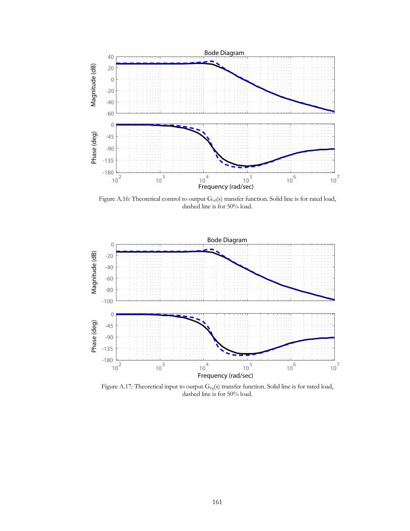
161
-60
-40
-20
0
20
40
Mag
nit
ud
e (d
B)
102
103
104
105
106
107
-180
-135
-90
-45
0
Phas
e (d
eg)
Frequency (rad/sec)
Bode Diagram
Figure A.16: Theoretical control to output Gvd(s) transfer function. Solid line is for rated load,
dashed line is for 50% load.
-100
-80
-60
-40
-20
0
Mag
nit
ud
e (d
B)
Frequency (rad/sec)
102
103
104
105
106
107
-180
-135
-90
-45
0
Phas
e (d
eg)
Frequency (rad/sec)
Bode Diagram
Figure A.17: Theoretical input to output Gvg(s) transfer function. Solid line is for rated load,
dashed line is for 50% load.
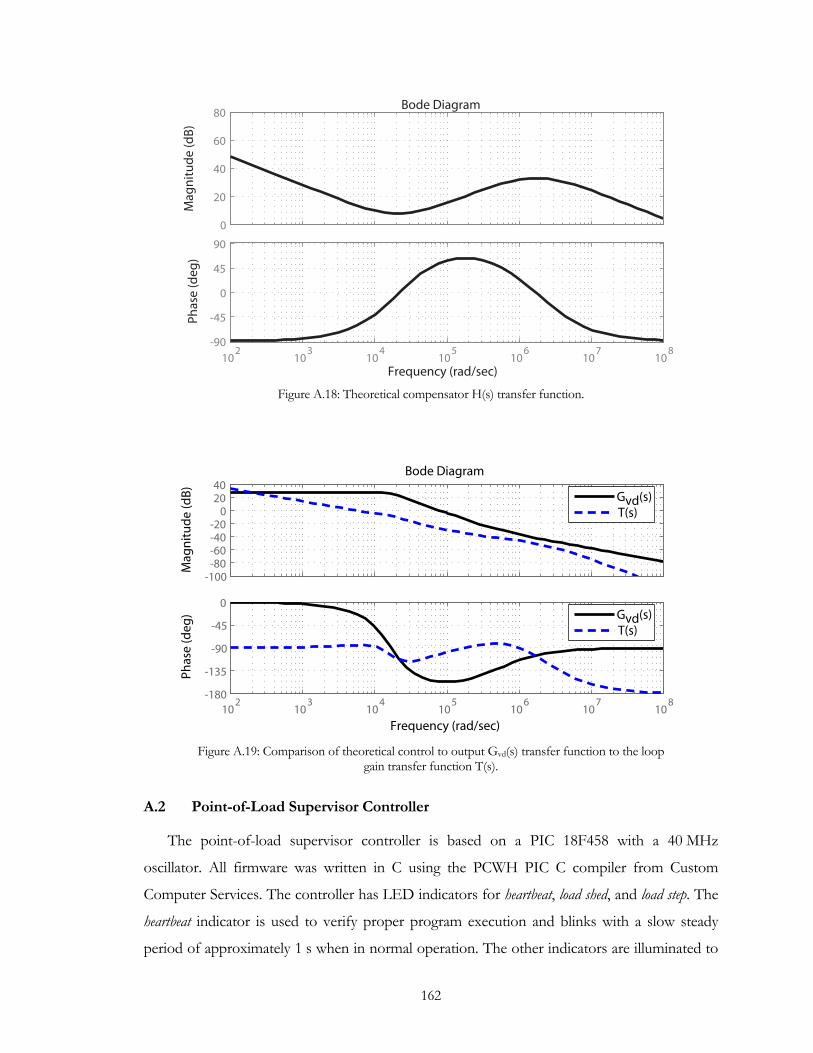
162
0
20
40
60
80
Mag
nit
ud
e (d
B)
102
103
104
105
106
107
108
-90
-45
0
45
90
Phas
e (d
eg)
Frequency (rad/sec)
Bode Diagram
Figure A.18: Theoretical compensator H(s) transfer function.
-100-80-60-40-20
02040
Mag
nit
ud
e (d
B)
Frequency (rad/sec)Frequency (rad/sec)
102
103
104
105
106
107
108
-180
-135
-90
-45
0
Phas
e (d
eg)
Frequency (rad/sec)
Bode Diagram
Gvd(s)T(s)
Gvd(s)T(s)
Figure A.19: Comparison of theoretical control to output Gvd(s) transfer function to the loop
gain transfer function T(s).
A.2 Point-of-Load Supervisor Controller
The point-of-load supervisor controller is based on a PIC 18F458 with a 40 MHz
oscillator. All firmware was written in C using the PCWH PIC C compiler from Custom
Computer Services. The controller has LED indicators for heartbeat, load shed, and load step. The
heartbeat indicator is used to verify proper program execution and blinks with a slow steady
period of approximately 1 s when in normal operation. The other indicators are illuminated to
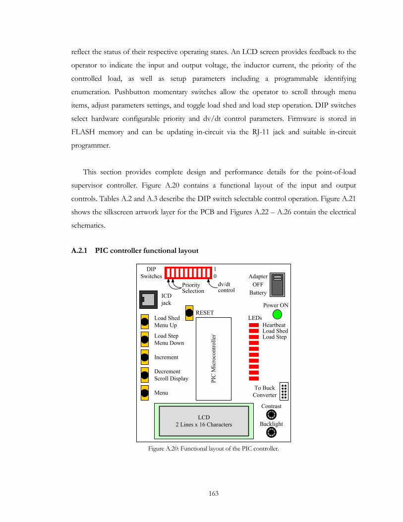
163
reflect the status of their respective operating states. An LCD screen provides feedback to the
operator to indicate the input and output voltage, the inductor current, the priority of the
controlled load, as well as setup parameters including a programmable identifying
enumeration. Pushbutton momentary switches allow the operator to scroll through menu
items, adjust parameters settings, and toggle load shed and load step operation. DIP switches
select hardware configurable priority and dv/dt control parameters. Firmware is stored in
FLASH memory and can be updating in-circuit via the RJ-11 jack and suitable in-circuit
programmer.
This section provides complete design and performance details for the point-of-load
supervisor controller. Figure A.20 contains a functional layout of the input and output
controls. Tables A.2 and A.3 describe the DIP switch selectable control operation. Figure A.21
shows the silkscreen artwork layer for the PCB and Figures A.22 – A.26 contain the electrical
schematics.
A.2.1 PIC controller functional layout
PIC
Mic
roco
ntro
ller
Load ShedMenu Up
Load StepMenu Down
Increment
DecrementScroll Display
Menu
HeartbeatLoad ShedLoad Step
Power ON
OFFAdapter
Battery
Contrast
Backlight
To Buck Converter
ICDjack
DIP Switches
dv/dtcontrol
LEDs
LCD2 Lines x 16 Characters
LCD2 Lines x 16 Characters
RESET
PrioritySelection
10
Figure A.20: Functional layout of the PIC controller.

164
Table A.2: Priority configuration.
Switch 1 2 Priority
0 0 Essential (High) 1 0 Semi-Essential (Med) 0 1 NonEssential (Low) 1 1 No Control
Table A.3: dv/dt control configuration.
Switch 8
dv/dt mode
0 Disable 1 Enable
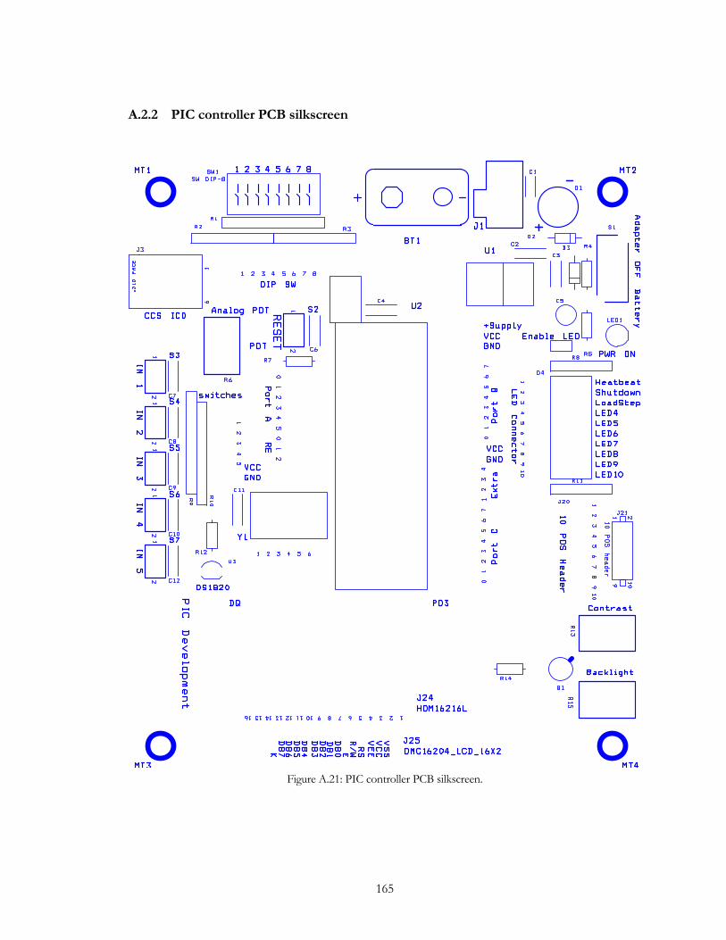
165
A.2.2 PIC controller PCB silkscreen
Figure A.21: PIC controller PCB silkscreen.
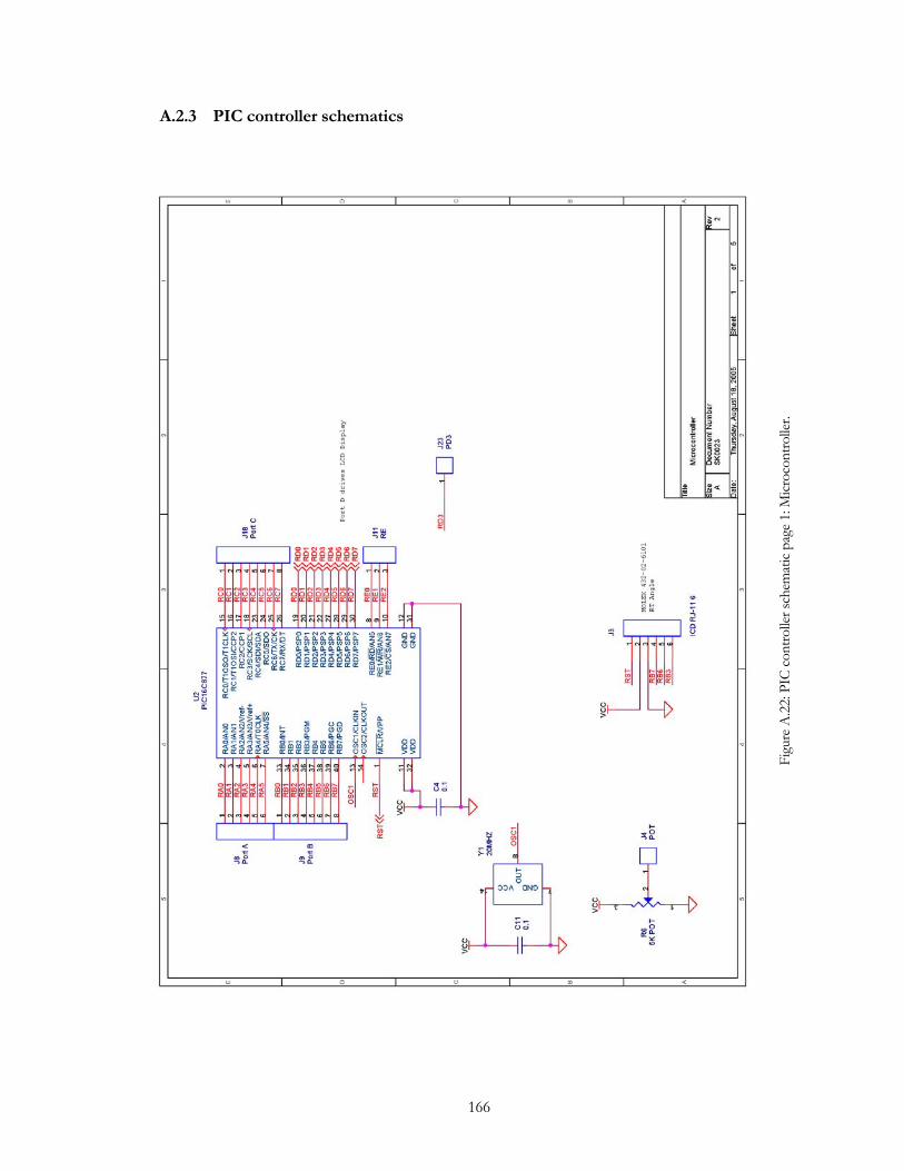
166
A.2.3 PIC controller schematics
Figu
re A
.22:
PIC
cont
rolle
r sch
emat
ic pa
ge 1
: Micr
ocon
trolle
r.
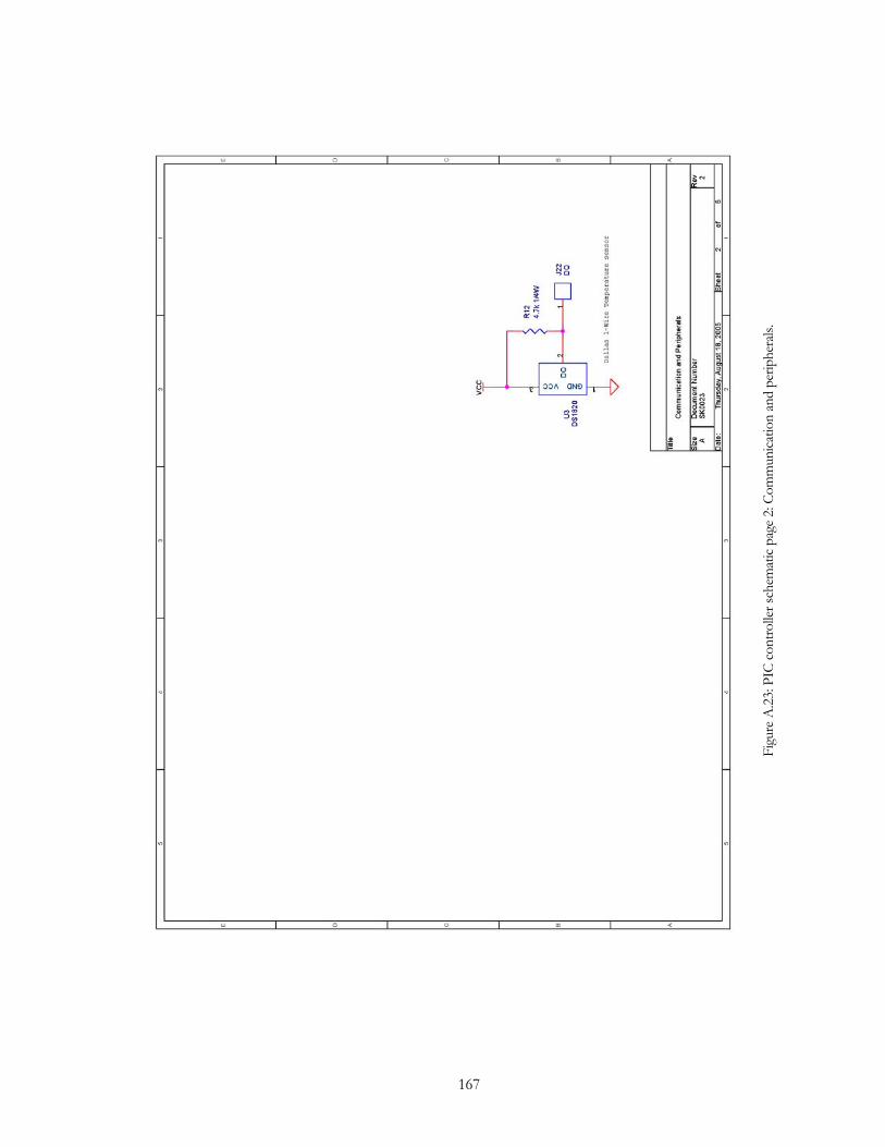
167
Figu
re A
.23:
PIC
cont
rolle
r sch
emat
ic pa
ge 2
: Com
mun
icatio
n an
d pe
riphe
rals.
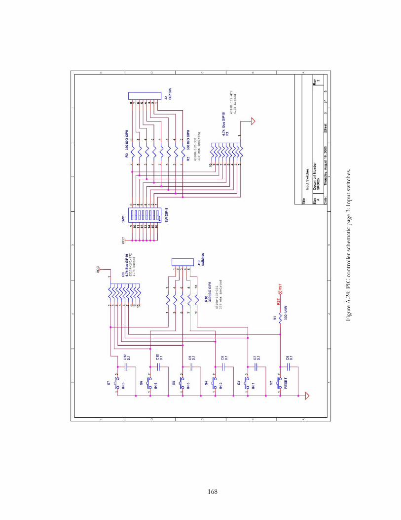
168
Figu
re A
.24:
PIC
cont
rolle
r sch
emat
ic pa
ge 3
: Inp
ut sw
itche
s.
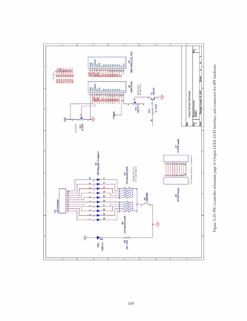
169
Figu
re A
.25:
PIC
cont
rolle
r sch
emat
ic pa
ge 4
: Out
put L
EDs,
LCD
inte
rface
, and
conn
ecto
r for
SPI
har
dwar
e.
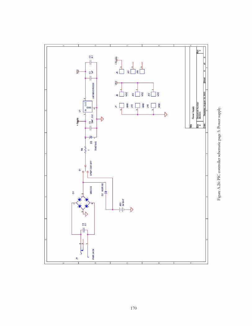
170
Figu
re A
.26:
PIC
cont
rolle
r sch
emat
ic pa
ge 5
: Pow
er su
pply.
171
A.3 Supervisor Control Firmware
This section contains the code listing for the firmware in the point-of-load supervisor
controller. Section A.3.1 is the main program. Section A.3.2 is the hardware driver for the
LCD display.
A.3.1 Main program
////////////////////////////////////////////////////////////////////////// ////////////////////////////////////////////////////////////////////////// //// EPNES DC SMPS Ver 1.00 //// //// Distributed Load-Side Controller //// //// //// //// Uses PB0023 Rev B PIC Controller PCB //// //// PB0019 Rev C Buck Converter PCB //// //// //// //// (2) MCP3202 12 bit dual channel A/D via Hardware SPI //// //// CH0 = (ADC0 CH0) Vin //// //// CH1 = (ADC0 CH1) N/A //// //// CH2 = (ADC1 CH0) I inductor //// //// CH3 = (ADC1 CH1) Vout //// //// //// //// Interrupt driven sampling, 926.4 us period //// //// Scrollable Menu via 2x16 char LCD display //// //// Calibration parameters setup via startup menu //// //// main loop xxxxx ms //// //// //// //// PORTA pinout //// //// A0 Button 3 A4 n/c //// //// A1 Button 4 A5 n/c //// //// A2 Button 5 //// //// A3 dV/dt control //// //// PORTB pinout //// //// B0 LoadStep LED B4 Load Step (button 2) //// //// B1 Shutdown LED B5 Load Shed (button 1) //// //// B2 Heartbeat LED B6 RESERVED (ICD) //// //// B3 RESERVED (ICD) B7 Enable Loadshed (ICD) //// //// PORTC pinout //// //// C0 CS~ DPOT C4 DIN //// //// C1 CS~ ADO C5 DOUT //// //// C2 CS~ AD1 C6 LOADSTEP //// //// C3 CLK C7 SHUTDOWN //// //// PORTD pinout //// //// See LCD subroutine //// //// //// //// EE Memory Map (LSByte, MSByte) //// //// Converter Parameters //// //// Bytes 000 - 000 Converter Name //// //// //// //// Calibration Parameters //// //// Bytes 010 - 011 Vin Scale //// //// Bytes 012 - 013 Vin Offset //// //// Bytes 014 - 015 Vout Scale //// //// Bytes 016 - 017 Vout Offset //// //// Bytes 018 - 019 Iout Scale //// //// Bytes 01A - 01B Iout Offset //// //// //// //// Controller Parameters ////

172
//// Bytes 040 - 041 Vmin limit Low Priority //// //// Bytes 042 - 043 Vmax limit Low Priority //// //// Bytes 044 - 045 neg dV/dt Low Priority //// //// Bytes 050 - 051 Vmin limit Med Priority //// //// Bytes 052 - 053 Vmax limit Med Priority //// //// Bytes 054 - 055 neg dV/dt Med Priority //// //// Bytes 060 - 061 Vmin limit High Priority //// //// Bytes 062 - 063 Vmax limit High Priority //// //// Bytes 064 - 065 neg dV/dt High Prioroty //// //// //// ////////////////////////////////////////////////////////////////////////// //// (C) Copyright 2005 Robert S. Balog Jr. //// //// and David H. Schmitz //// ////////////////////////////////////////////////////////////////////////// #include <18F458.h> #define version "1.00" //Firmware version #device *=16 //16 bit pointers #device ICD=TRUE //ALLOW ICD #use delay(clock=40000000,RESTART_WDT) //40 MHz clock #FUSES WDT //Watch Dog Timer #FUSES HS //High speed Osc (> 4mhz) #FUSES PUT //Power Up Timer #FUSES NOPROTECT //Code not protected from reading #FUSES BROWNOUT //Reset when brownout detected #FUSES STVREN //Stack full/underflow reset #FUSES LVP //Low Volt Prog on B3(PIC16) #FUSES NOCPD //No EE protection #FUSES NOWRT //Prog memory not write protected #FUSES DEBUG //Debug mode for use with ICD #include <LCD_RSB.c> //LCD routines #include <STDLIB.H> //Standard IO library // LCD Port definition #if defined(__PCH__) //Port memory addresses #byte portb = 0xF81 //port B for 18F series #else #byte portb=0x06 //port B for 16F series #endif //#bit MLT = portb.3 //Main Loop Timer LED #bit HB_LED = portb.2 //Heartbeat LED int16 loopcnt=0; //Heartbeat counter #define LS_LED PIN_B0 //Loadstep LED #define SHTDN_LED PIN_B1 //Shutdown LED #define LS_BUT PIN_B4 //Enable loadshed button #define SHTDN_BUT PIN_B5 //Shutdown gate signal button #define P1 PIN_B7 //Controller enable #define P2 PIN_B6 //Controller enable #define DVDT PIN_A3 //dV/dt control enable #define ADC0 PIN_C1 //CS ADC0 #define ADC1 PIN_C2 //CS ADC1 #define LS PIN_C6 //Load Step #define SHTDN PIN_C7 //Gate Driver SHUTDOWN int1 LOADSTEP = 0; //toggle switch action to step int1 SHUTDOWN = 0; //toggle switch action to shed // Define pushbutton pin mappings #define BTN1 PIN_B5 #define BTN2 PIN_B4 #define BTN3 PIN_A0 #define BTN4 PIN_A1

173
#define BTN5 PIN_A2 // Button variables int1 button1_old, button2_old; //registers for button debouce int1 button3_old, button4_old; //registers for button debouce int1 button5_old; //registers for button debouce int1 button1_state, button2_state; //state of button - 0 when pressed int1 button3_state, button4_state; //state of button - 0 when pressed int1 button5_state; //state of button - 0 when pressed int1 b1_toggle, b2_toggle, b3_toggle; //Toggle buttons int1 b4_toggle, b5_toggle; //Toggle buttons int8 inc_but, inc_cnt; //Adjustable button increment speed int16 button_slow = 0; //counter to make sure updates on //buttons only occur at set interval #define BUTTON_LIM 500 //reset value for button_slow // Define Priority Names #define PRIORITY0 "None " #define PRIORITY1 "Low " #define PRIORITY2 "Med " #define PRIORITY3 "High " const char priority_title[4][17] = PRIORITY0, PRIORITY1, PRIORITY2, PRIORITY3; // EEPROM Data info #define NUMSETPARAM 6 //num of Setup parameters #define NUMPRIPARAM 3 //num of Priority parameters #define NUMPRI 3 //num of Priorities #define NUMCONPARAM 1 //num of Converter Parameters #define CONINFOFF 0x00 //Offset of Converter Info Param #define SETPAROFF 0x10 //Offset of Setup parameters #define PRIOFF1 0x40 //Offset of Priority 1 parameters #define PRIOFF2 0x50 //Offset of Priority 2 parameters #define PRIOFF3 0x60 //Offset of Priority 3 parameters const int PRIOFFS[] = PRIOFF1, PRIOFF2, PRIOFF3; //Array of Priority offsets //#define DPAROFF //Offset of Dynamic parameters // Variables for the ADC process #define CH0len 240 //length of averaging array #define CH2len 32 //length of averaging array #define CH3len 24 //length of averaging array #define NEGMAX -20 //Max neg dvdt for load shed // Dwell Time Counters - # of interupt periods #define T_THRES 100 //CH0 > Vmax and load EN #define Toff_THRES 500 //CH0 < Vmin and load Shed unsigned int16 value_ch0[CH0len], ch0, ch0_ave, ch0_noave; int16 deriv_ch0[CH0len]; //ch0 d/dt values int16 max_deriv, min_deriv; int16 deriv0_avg; //ave of ch0 d/dt values int16 milsecs1 = 0, milsecs2 = 0; //ellapsed mS cntr - reset manually int16 milsecs_off; //dwell before off int1 counten1 = 0, counten2 = 0; //flag for dwell ON mS counter int1 counten_off = 0; //flag for dwell OFF mS counter unsigned int16 value_ch2[CH2len], ch2, ch2_ave; unsigned int16 value_ch3[CH3len], ch3, ch3_ave; int32 A1 = 0, B1 = 0, C1 = 0; //Filter parameters int1 ch0_update=1; //update flag for Display int1 ch2_update=1; //update flag for Display int1 ch3_update=1; //update flag for Display

174
int16 ADC00, ADC10, ADC11; //ADC 1 CH 0 &1 int upper, lower; //temp bytes for ADC int8 pntr_ch0=0, pntr_ch2=0; //pointer into arrays int8 pntr_ch3=0, dindex_ch0=0; ldiv_t vch0fmt; //*.quot & *.rem structure ldiv_t vch2fmt; //*.quot & *.rem structure ldiv_t vch3fmt; //*.quot & *.rem structure // MENU Control int8 menutime= 0; //Time in a menu int1 scrollmenu = 0; //toggle switch to scroll menu down int8 topline = 0;
//LCD top line int8 botline = 1; //LCD bottom line int1 run_setpointmenu =0; //flag for setpoint menu - 0 in menu int1 run_update=1; //flag to update runtime menu int1 menu_update = 1; //General menu update flag #define MENUSIZE 4 #define DCHAN0 4 //Difference between displayed and #define DCHAN2 15 //current values for update to occur #define DCHAN3 4 // Define Menu Titles #define MENU0 "Vin " #define MENU1 "Iout " #define MENU2 "Vout " #define MENU3 "Priority " // Define array of Menu titles const char menu_titles[MENUSIZE][17] = MENU0, MENU1, MENU2, MENU3; ////////////////////////////////////////////////////////////////////////// // Function Prototypes ////////////////////////////// ////////////////////////////////////////////////////////////////////////// //LED & LCD initialiation void LED_init(); void lcd_splash(); void lcd_menu0(); void lcd_menu1_setup(); //power on setup menu void setup_menu(); //runtime setup menu void setpointmenu(int &menu_state, int16 iv_param[]); //Low Pass filter for measured inputs, stores intermediate values to A1,B1,C1 unsigned int16 filter(unsigned int16 input); ////////////////////////////////////////////////////////////////////////// // Timer Interrupt, interrupt period controlled w/in main loop ///////// ////////////////////////////////////////////////////////////////////////// #INT_TIMER2 void sample() // Capture data from A/D chip via SPI // Read ADC 0 Ch 0 ////////////////////////////////// output_low(ADC0); //enable CS spi_write( 12 ); //Start Conversion upper=spi_read( 0 ); //Read upper byte lower=spi_read( 0 ); //Read lower byte output_high(ADC0); //disable CS ADC00 = make16(upper,lower)>>3; //Make 12 bit result // Read ADC 1 Ch 0 ////////////////////////////////// output_low(ADC1); //enable CS

175
spi_write( 12 ); //Start Conversion upper=spi_read( 0 ); //Read upper byte lower=spi_read( 0 ); //Read lower byte output_high(ADC1); //disable CS ADC10 = make16(upper,lower)>>3; //Make 12 bit result // Read ADC 1 Ch 1 ////////////////////////////////// output_low(ADC1); //enable CS spi_write( 14 ); //Start Conversion upper=spi_read( 0 ); //Read upper byte lower=spi_read( 0 ); //Read lower byte output_high(ADC1); //disable CS ADC11 = make16(upper,lower)>>3; //Make 12 bit result // Read & filter data on ADC 0 Ch 1 ////////////////////////////////// pntr_ch0++; if (pntr_ch0==CH0len) pntr_ch0=0; //when pntr=end+1 reset to 0 value_ch0[pntr_ch0] = ADC00; //store to circular buffer ch0_ave = filter(ADC00); //low pass filter present sample // Increment inturrupt counters ////////////////////////////////// if(counten1) milsecs1++; if(counten2) milsecs2++; if(counten_off) milsecs_off++; ////////////////////////////////////////////////////////////////////////// ////////////////////////////////////////////////////////////////////////// //////////////////// MAIN PROGRAM //////////////////// ////////////////////////////////////////////////////////////////////////// ////////////////////////////////////////////////////////////////////////// void main() unsigned int32 sum; //summation for A/D averaging unsigned int16 last_ch0; //temp variable for channel unsigned int16 last_ch2; // average being displayed unsigned int16 last_ch3; int16 stat_iv_param[NUMPRIPARAM*NUMPRI]; //local copy of Priority EE param int16 set_iv_param[NUMSETPARAM]; //local copy of setup EE param int1 pinstat; int8 i,n; //general variable int1 der; //derivative flag int8 priority, last_priority; //Priority variable int menu_state = 0; //State for tracking menu lcd_init(); //LCD initialization routine lcd_splash(); //Startup LCD splash screen led_init(); //call cycle led routine // Initialize SPI ////////////////////////////// //DIV_16 -> 1.25MHz @ 20MHz crystal //Clock idle is low //clock is low to high transition setup_spi(SPI_MASTER | SPI_L_TO_H | SPI_CLK_DIV_16 |SPI_XMIT_L_TO_H); output_high(ADC0); //Initialization output_high(ADC1); //Initialization delay_ms(1000); lcd_menu0(); //Splash Screen with code VER delay_ms(1000); lcd_menu1_setup(); // Initialize Timer ////////////////////////////// //Timer pulses every 1.6us (DIV16), overflow every 308.8us (0xC0) //and triggers interrupt every 926.4us (3*0xC0) setup_timer_2(T2_DIV_BY_16, 0xC0, 3); enable_interrupts(GLOBAL); //enable interrupts

176
enable_interrupts(INT_TIMER2); //enable timer interrupt // Enter Power-On SETUP menu ////////////////////////////// //Set Tristate to detect button inputs set_tris_b(0b11110000); set_tris_a(0xFF); pinstat = input( BTN5 ); //Test for button press delay_us(150); pinstat = (pinstat || input(BTN5)); //Debounce if (pinstat==0) setup_menu(); // Read Parameters from EEPROM ////////////////////////////// //Read Priority Parameters for (i = 0; i < NUMPRI; i++) for (loopcnt = 0; loopcnt < (NUMPRIPARAM*2); loopcnt++) *(&stat_iv_param[NUMPRIPARAM*i]+loopcnt)=read_eeprom(loopcnt+PRIOFFS[i]); //Read Setup Parameters for (loopcnt = 0; loopcnt < (NUMSETPARAM*2); loopcnt++) *(&set_iv_param[0] + loopcnt) = read_eeprom(loopcnt+SETPAROFF); // Turn on converter ////////////////////////////// output_low(SHTDN_LED); //turn on converter LED output_low(SHTDN); //turn on converter ////////////////////////////////////////////////////////////////////////// ////////////////////// MAIN LOOP ////////////////////// ////////////////////////////////////////////////////////////////////////// while (true) // MLT=!MLT; //main loop timer IF (loopcnt==1024) HB_LED=!HB_LED; //Heartbeat LED loopcnt=0; menutime++; loopcnt++; //Increment heartbeat counter ////////////////////////////////////////////////////////////////////////// // Debounce Buttons ////////////////////////////// button1_state = (button1_old || input(BTN1)); // 0 = btn pressed button2_state = (button2_old || input(BTN2)); button3_state = (button3_old || input(BTN3)); button4_state = (button4_old || input(BTN4)); button5_state = (button5_old || input(BTN5)); button1_old = input(BTN1); button2_old = input(BTN2); button3_old = input(BTN3); button4_old = input(BTN4); button5_old = input(BTN5); // Act on button press, not depress if(!button1_state && b1_toggle) //Load SHED b1_toggle = 0; if(!run_setpointmenu) SHUTDOWN=!SHUTDOWN;
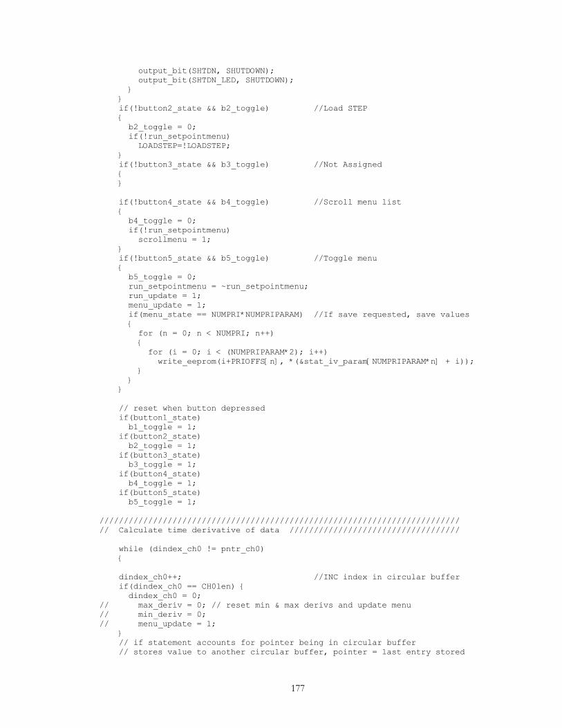
177
output_bit(SHTDN, SHUTDOWN); output_bit(SHTDN_LED, SHUTDOWN); if(!button2_state && b2_toggle) //Load STEP b2_toggle = 0; if(!run_setpointmenu) LOADSTEP=!LOADSTEP; if(!button3_state && b3_toggle) //Not Assigned if(!button4_state && b4_toggle) //Scroll menu list b4_toggle = 0; if(!run_setpointmenu) scrollmenu = 1; if(!button5_state && b5_toggle) //Toggle menu b5_toggle = 0; run_setpointmenu = ~run_setpointmenu; run_update = 1; menu_update = 1; if(menu_state == NUMPRI*NUMPRIPARAM) //If save requested, save values for (n = 0; n < NUMPRI; n++) for (i = 0; i < (NUMPRIPARAM*2); i++) write_eeprom(i+PRIOFFS[n], *(&stat_iv_param[NUMPRIPARAM*n] + i)); // reset when button depressed if(button1_state) b1_toggle = 1; if(button2_state) b2_toggle = 1; if(button3_state) b3_toggle = 1; if(button4_state) b4_toggle = 1; if(button5_state) b5_toggle = 1; ////////////////////////////////////////////////////////////////////////// // Calculate time derivative of data /////////////////////////////////// while (dindex_ch0 != pntr_ch0) dindex_ch0++; //INC index in circular buffer if(dindex_ch0 == CH0len) dindex_ch0 = 0; // max_deriv = 0; // reset min & max derivs and update menu // min_deriv = 0; // menu_update = 1; // if statement accounts for pointer being in circular buffer // stores value to another circular buffer, pointer = last entry stored

178
// 1079 multiplier based on dt value of 926.4 us if(pntr_ch0 == 0) // deriv_ch0[dindex_ch0] = (value_ch0[0] - value_ch0[CH0len-1]) * // (int32)5395 * set_iv_param[0] / (int32)4095; deriv_ch0[dindex_ch0] = (value_ch0[0] - value_ch0[CH0len-4]); else if(pntr_ch0 == 1) deriv_ch0[dindex_ch0] = (value_ch0[1] - value_ch0[CH0len-3]); else if(pntr_ch0 == 2) deriv_ch0[dindex_ch0] = (value_ch0[2] - value_ch0[CH0len-2]); else if(pntr_ch0 == 3) deriv_ch0[dindex_ch0] = (value_ch0[3] - value_ch0[CH0len-1]); else // attempt at scaling to real values // deriv_ch0[dindex_ch0] = (value_ch0[pntr_ch0] - value_ch0[pntr_ch0-1]) // * (int32)5395 * set_iv_param[0] / (int32)4095; deriv_ch0[dindex_ch0] = (value_ch0[pntr_ch0] - value_ch0[pntr_ch0-4]); // Throw out entries under negative threshold - voltage spikes if ((signed int16)deriv_ch0[dindex_ch0] < (signed int16)NEGMAX) deriv_ch0[dindex_ch0] = 0; // Track maximum and minimum derivative values // if((signed int16)deriv_ch0[dindex_ch0] > (signed int16)max_deriv) // max_deriv = deriv_ch0[dindex_ch0]; // if((signed int16)deriv_ch0[dindex_ch0] < (signed int16)min_deriv) // min_deriv = ((signed int16)deriv_ch0[dindex_ch0]); //perform 4 entry windowed average on derivative if (dindex_ch0 == 0) deriv0_avg = (signed int16)(deriv_ch0[0] + deriv_ch0[CH0len-1] + deriv_ch0[CH0len-2] + deriv_ch0[CH0len-3])/4; else if (dindex_ch0 == 1) deriv0_avg = (signed int16)(deriv_ch0[0] + deriv_ch0[CH0len-1] + deriv_ch0[CH0len-2] + deriv_ch0[1])/4; else if (dindex_ch0 == 2) deriv0_avg = (signed int16)(deriv_ch0[0] + deriv_ch0[CH0len-1] + deriv_ch0[1] + deriv_ch0[2])/4; else deriv0_avg = (signed int16)(deriv_ch0[dindex_ch0] + deriv_ch0[dindex_ch0-1] + deriv_ch0[dindex_ch0-2] + deriv_ch0[dindex_ch0-3])/4; // determine when to update display if (abs(ch0_ave - last_ch0)>DCHAN0) ch0_update = 1; //update display flag ch0 = (set_iv_param[0] * 5 * (int32)ch0_ave) / (int32)4095; ch0_noave = ch0; vch0fmt = ldiv(ch0,1000); ////////////////////////////////////////////////////////////////////////// // Average A/D conversions on AD1 CH0 ->ch2 //////////////////////////// value_ch2[pntr_ch2++] = ADC10<<2; //use a circular pointer if (pntr_ch2==CH2len) pntr_ch2=0; //when pntr=end+1 reset to 0 sum=0; for (i=0; i<CH2len; i++) sum+=(int32)value_ch2[i]; ch2_ave=(sum/(int32)CH2len)>>2; if (abs(ch2_ave - last_ch2)>DCHAN2) ch2_update = 1; //update display flag ch2 = (set_iv_param[4]*5*(int32)(ch2_ave-set_iv_param[5]))
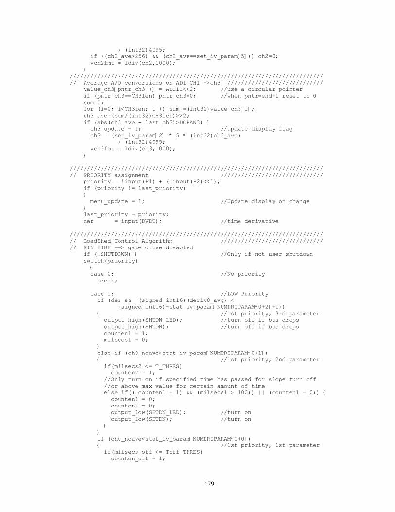
179
/ (int32)4095; if ((ch2_ave>256) && (ch2_ave==set_iv_param[5])) ch2=0; vch2fmt = ldiv(ch2,1000); ////////////////////////////////////////////////////////////////////////// // Average A/D conversions on AD1 CH1 ->ch3 //////////////////////////// value_ch3[pntr_ch3++] = ADC11<<2; //use a circular pointer if (pntr_ch3==CH3len) pntr_ch3=0; //when pntr=end+1 reset to 0 sum=0; for (i=0; i<CH3len; i++) sum+=(int32)value_ch3[i]; ch3_ave=(sum/(int32)CH3len)>>2; if (abs(ch3_ave - last_ch3)>DCHAN3) ch3_update = 1; //update display flag ch3 = (set_iv_param[2] * 5 * (int32)ch3_ave) / (int32)4095; vch3fmt = ldiv(ch3,1000); ////////////////////////////////////////////////////////////////////////// // PRIORITY assignment ////////////////////////////// priority = !input(P1) + (!input(P2)<<1); if (priority != last_priority) menu_update = 1; //Update display on change last_priority = priority; der = input(DVDT); //time derivative ////////////////////////////////////////////////////////////////////////// // LoadShed Control Algorithm ////////////////////////////// // PIN HIGH ==> gate drive disabled if (!SHUTDOWN) //Only if not user shutdown switch(priority) case 0: //No priority break; case 1: //LOW Priority if (der && ((signed int16)(deriv0_avg) < (signed int16)~stat_iv_param[NUMPRIPARAM*0+2]+1)) //1st priority, 3rd parameter output_high(SHTDN_LED); //turn off if bus drops output_high(SHTDN); //turn off if bus drops counten1 = 1; milsecs1 = 0; else if (ch0_noave>stat_iv_param[NUMPRIPARAM*0+1]) //1st priority, 2nd parameter if(milsecs2 <= T_THRES) counten2 = 1; //Only turn on if specified time has passed for slope turn off //or above max value for certain amount of time else if(((counten1 = 1) && (milsecs1 > 100)) || (counten1 = 0)) counten1 = 0; counten2 = 0; output_low(SHTDN_LED); //turn on output_low(SHTDN); //turn on if (ch0_noave<stat_iv_param[NUMPRIPARAM*0+0]) //1st priority, 1st parameter if(milsecs_off <= Toff_THRES) counten_off = 1;
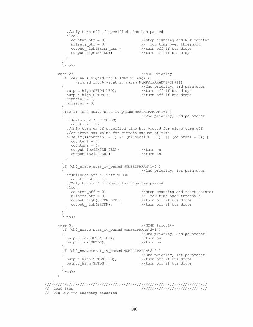
180
//Only turn off if specified time has passed else counten_off = 0; //stop counting and RST counter milsecs_off = 0; // for time over threshold output_high(SHTDN_LED); //turn off if bus drops output_high(SHTDN); //turn off if bus drops break; case 2: //MED Priority if (der && ((signed int16)(deriv0_avg) < (signed int16)~stat_iv_param[NUMPRIPARAM*1+2]+1)) //2nd priority, 3rd parameter output_high(SHTDN_LED); //turn off if bus drops output_high(SHTDN); //turn off if bus drops counten1 = 1; milsecs1 = 0; else if (ch0_noave>stat_iv_param[NUMPRIPARAM*1+1]) //2nd priority, 2nd parameter if(milsecs2 <= T_THRES) counten2 = 1; //Only turn on if specified time has passed for slope turn off //or above max value for certain amount of time else if(((counten1 = 1) && (milsecs1 > 100)) || (counten1 = 0)) counten1 = 0; counten2 = 0; output_low(SHTDN_LED); //turn on output_low(SHTDN); //turn on if (ch0_noave<stat_iv_param[NUMPRIPARAM*1+0]) //2nd priority, 1st parameter if(milsecs_off <= Toff_THRES) counten_off = 1; //Only turn off if specified time has passed else counten_off = 0; //stop counting and reset counter milsecs_off = 0; // for time over threshold output_high(SHTDN_LED); //turn off if bus drops output_high(SHTDN); //turn off if bus drops break; case 3: //HIGH Priority if (ch0_noave>stat_iv_param[NUMPRIPARAM*2+1]) //3rd priority, 2nd parameter output_low(SHTDN_LED); //turn on output_low(SHTDN); //turn on if (ch0_noave<stat_iv_param[NUMPRIPARAM*2+0]) //3rd priority, 1st parameter output_high(SHTDN_LED); //turn off if bus drops output_high(SHTDN); //turn off if bus drops break; ////////////////////////////////////////////////////////////////////////// // Load Step ////////////////////////////// // PIN LOW ==> Loadstep disabled
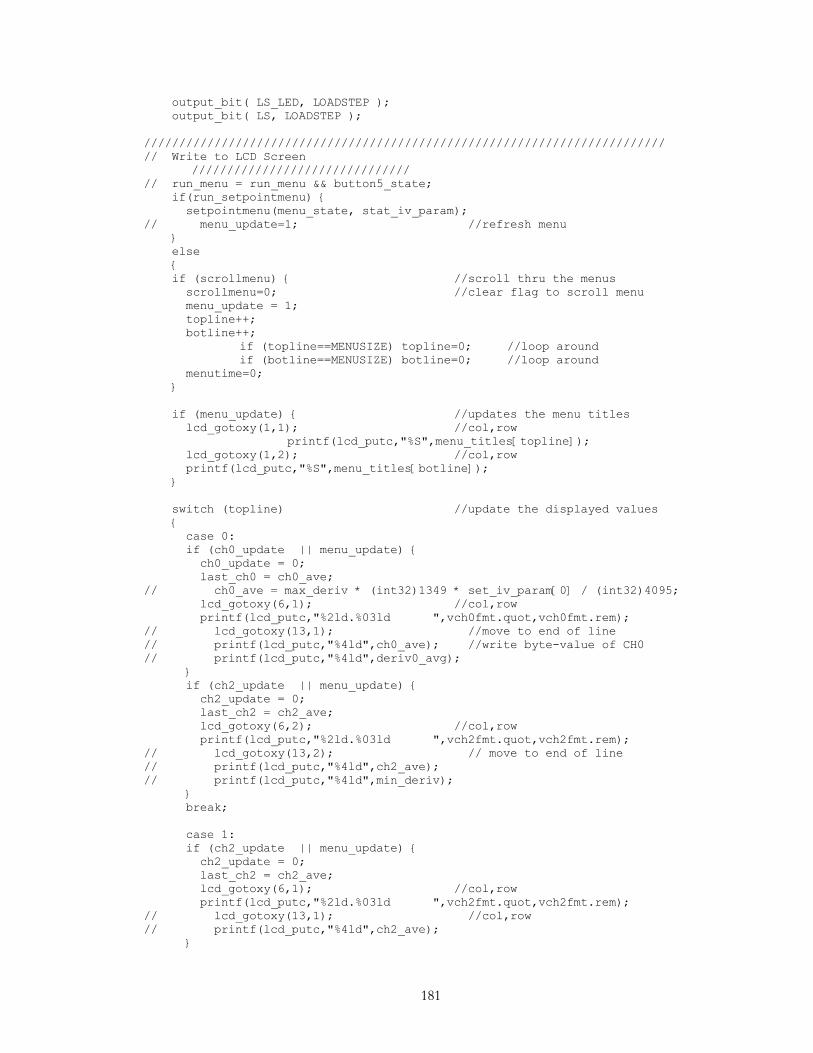
181
output_bit( LS_LED, LOADSTEP ); output_bit( LS, LOADSTEP ); ////////////////////////////////////////////////////////////////////////// // Write to LCD Screen
/////////////////////////////// // run_menu = run_menu && button5_state; if(run_setpointmenu) setpointmenu(menu_state, stat_iv_param); // menu_update=1; //refresh menu else if (scrollmenu) //scroll thru the menus scrollmenu=0; //clear flag to scroll menu menu_update = 1; topline++; botline++; if (topline==MENUSIZE) topline=0; //loop around if (botline==MENUSIZE) botline=0; //loop around menutime=0; if (menu_update) //updates the menu titles lcd_gotoxy(1,1); //col,row printf(lcd_putc,"%S",menu_titles[topline]); lcd_gotoxy(1,2); //col,row printf(lcd_putc,"%S",menu_titles[botline]); switch (topline) //update the displayed values case 0: if (ch0_update || menu_update) ch0_update = 0; last_ch0 = ch0_ave; // ch0_ave = max_deriv * (int32)1349 * set_iv_param[0] / (int32)4095; lcd_gotoxy(6,1); //col,row printf(lcd_putc,"%2ld.%03ld ",vch0fmt.quot,vch0fmt.rem); // lcd_gotoxy(13,1); //move to end of line // printf(lcd_putc,"%4ld",ch0_ave); //write byte-value of CH0 // printf(lcd_putc,"%4ld",deriv0_avg); if (ch2_update || menu_update) ch2_update = 0; last_ch2 = ch2_ave; lcd_gotoxy(6,2); //col,row printf(lcd_putc,"%2ld.%03ld ",vch2fmt.quot,vch2fmt.rem); // lcd_gotoxy(13,2); // move to end of line // printf(lcd_putc,"%4ld",ch2_ave); // printf(lcd_putc,"%4ld",min_deriv); break; case 1: if (ch2_update || menu_update) ch2_update = 0; last_ch2 = ch2_ave; lcd_gotoxy(6,1); //col,row printf(lcd_putc,"%2ld.%03ld ",vch2fmt.quot,vch2fmt.rem); // lcd_gotoxy(13,1); //col,row // printf(lcd_putc,"%4ld",ch2_ave);
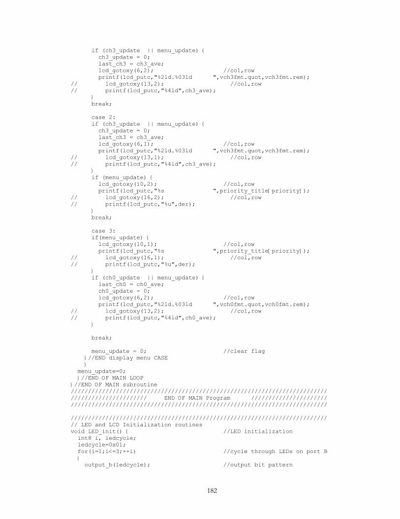
182
if (ch3_update || menu_update) ch3_update = 0; last_ch3 = ch3_ave; lcd_gotoxy(6,2); //col,row printf(lcd_putc,"%2ld.%03ld ",vch3fmt.quot,vch3fmt.rem); // lcd_gotoxy(13,2); //col,row // printf(lcd_putc,"%4ld",ch3_ave); break; case 2: if (ch3_update || menu_update) ch3_update = 0; last_ch3 = ch3_ave; lcd_gotoxy(6,1); //col,row printf(lcd_putc,"%2ld.%03ld ",vch3fmt.quot,vch3fmt.rem); // lcd_gotoxy(13,1); //col,row // printf(lcd_putc,"%4ld",ch3_ave); if (menu_update) lcd_gotoxy(10,2); //col,row printf(lcd_putc,"%s ",priority_title[priority]); // lcd_gotoxy(16,2); //col,row // printf(lcd_putc,"%u",der); break; case 3: if(menu_update) lcd_gotoxy(10,1); //col,row printf(lcd_putc,"%s ",priority_title[priority]); // lcd_gotoxy(16,1); //col,row // printf(lcd_putc,"%u",der); if (ch0_update || menu_update) last_ch0 = ch0_ave; ch0_update = 0; lcd_gotoxy(6,2); //col,row printf(lcd_putc,"%2ld.%03ld ",vch0fmt.quot,vch0fmt.rem); // lcd_gotoxy(13,2); //col,row // printf(lcd_putc,"%4ld",ch0_ave); break; menu_update = 0; //clear flag //END display menu CASE menu_update=0; //END OF MAIN LOOP //END OF MAIN subroutine ////////////////////////////////////////////////////////////////////////// ////////////////////// END OF MAIN Program ////////////////////// ////////////////////////////////////////////////////////////////////////// ////////////////////////////////////////////////////////////////////////// // LED and LCD Initialization routines void LED_init() //LED initialization int8 i, ledcycle; ledcycle=0x01; for(i=1;i<=3;++i) //cycle through LEDs on port B output_b(ledcycle); //output bit pattern

183
shift_left(&ledcycle,1,1); //shift in 1 as LSB delay_ms(100); output_b(0); //turn of all portb leds void lcd_splash() printf(lcd_putc,"\f Advanced Power "); printf(lcd_putc,"\n Laboratory "); void lcd_menu0() int id; id = read_eeprom(CONINFOFF); printf(lcd_putc,"\fSMPS Controller "); printf(lcd_putc,"\n Ver %S ID%3U",version,id); void lcd_menu1_setup() printf(lcd_putc,"\f%S",menu_titles[0]); printf(lcd_putc,"\n%S",menu_titles[1]); /////////////////////////////////////////////////////////////////////////// // Power-up SETUP MENU /////////////////////////////// void setup_menu() int1 delaymain = 1, menu_update = 1, but1,but2,but3,but4,but5; int menu_stat = 0, i,n; int const MENU_ENT = NUMPRIPARAM*NUMPRI+NUMSETPARAM+NUMCONPARAM+1; // Number of menu entries int16 iv_param[MENU_ENT-1]; //local copy of EE // Read values from EEPROM to array iv_param[] iv_param[0] = (int16)read_eeprom(CONINFOFF); // Read Converter Parameters for (n = 0; n < NUMPRI; n++) for (i = 0; i < (NUMPRIPARAM*2); i++) // Read Priority Params *(&iv_param[NUMCONPARAM+NUMPRIPARAM*n] + i) = read_eeprom(i+PRIOFFS[n]); for (i = 0; i < (NUMSETPARAM*2); i++) // Read Setup Params *(&iv_param[NUMCONPARAM+NUMPRIPARAM*NUMPRI] + i) = read_eeprom(i+SETPAROFF); printf(lcd_putc,"\f Setup Menu "); delay_ms(500); while (delaymain) IF (loopcnt==256) HB_LED=!HB_LED; //Heartbeat LED loopcnt=0; loopcnt++; //Increment heartbeat counter //Check for Button presses but1 = input( BTN1 ); //up arrow but2 = input( BTN2 ); //enter / accept but3 = input( BTN3 ); //down arrow but4 = input( BTN4 ); //increment but5 = input( BTN5 ); //decrement delay_us(500); but1 = (but1 || input(BTN1)); //debounce but2 = (but2 || input(BTN2)); //debounce but3 = (but3 || input(BTN3)); //debounce but4 = (but4 || input(BTN4)); //debounce

184
but5 = (but5 || input(BTN5)); //debounce //UP button pressed if ((but1 == 0) && (menu_stat > 0)) delay_ms(500); menu_stat--; // Decrement menu - go to top menu_update = 1; // Set flag to update menu //Select Button Pressed if (but5 == 0) switch (menu_stat) //Most cases do nothing when select pressed, // maybe could be used to reset value? case MENU_ENT-1: // Save data and exit menu // Write to EEPROM Converter Info write_eeprom(CONINFOFF, (int)iv_param[0]); // Write to EEPROM Priority Parameters for (n = 0; n < NUMPRI; n++) for (i = 0; i < NUMPRIPARAM*2; i++) write_eeprom(i+PRIOFFS[n], *(&iv_param[NUMCONPARAM+NUMPRIPARAM*n] + i)); // Write to EEPROM Setup Parameters for (i = 0; i < (NUMSETPARAM*2); i++) write_eeprom(i+SETPAROFF, *(&iv_param[NUMCONPARAM+NUMPRIPARAM*NUMPRI] + i)); // Set condition to quit while loop delaymain = 0; case MENU_ENT: // Exit menu only delaymain = 0; break; default: break; //DN button pressed //If menu entry is less than MENU_ENT, increment menu entry if ((but2 == 0) && (menu_stat < MENU_ENT)) //DN button pressed delay_ms(500); menu_stat++; menu_update = 1; // Right now increment and decrement buttons increase and decrease by 1 // if held for 10 cycles, they will increase and decrease by 10 // Inc button pressed // Increments array item value when pressed if ((but3 == 0) && (menu_stat < MENU_ENT)) // Check button and array range if ((i == 255) && (n < 40)) // If button was pressed previously, i=255 n++; // Track how long button is held

185
if ((n > 20) && (i == 255)) // If held for more than 10 cycles iv_param[menu_stat] += 100; // increment by 10 else if ((n > 10) && (i == 255)) // If held for more than 10 cycles iv_param[menu_stat] += 10; // increment by 10 else // Otherwise iv_param[menu_stat]++; // increment by 1 if (i != 255) // If i was not 255 i = 255; // set to 255 n = 0; // and reset hold counter delay_ms(200); menu_update = 1; // Dec button pressed // Decrements array item value when pressed // Works the same as above for button 4 except i is 254 if ((but4 == 0) && (menu_stat < MENU_ENT)) if ((i == 254) && (n < 40)) n++; if ((n > 20) && (i == 254)) iv_param[menu_stat] -= 100; else if ((n > 10) && (i == 254)) iv_param[menu_stat] -= 10; else iv_param[menu_stat]--; if (i != 254) i = 254; n = 0; delay_ms(200); menu_update = 1; // Check to see if neither increment or decrement pressed if ((but3 == 1) && (but4 == 1)) i = 0; // If neither button is pressed, i is 0 n = 0; // and hold counter is 0 too if (menu_update) menu_update = 0; // Set menu as updated switch (menu_stat) case 0: printf(lcd_putc,"\fConverter Name "); printf(lcd_putc,"\n %3U >",(int)iv_param[menu_stat]); break; case 1: printf(lcd_putc,"\fVmin limit Low <"); printf(lcd_putc,"\n%5ld >",iv_param[menu_stat]); break; case 2: printf(lcd_putc,"\fVmax limit Low <"); printf(lcd_putc,"\n%5ld >",iv_param[menu_stat]); break; case 3: printf(lcd_putc,"\fdV/dt neg Low <");
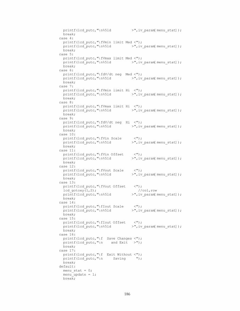
186
printf(lcd_putc,"\n%5ld >",iv_param[menu_stat]); break; case 4: printf(lcd_putc,"\fVmin limit Med <"); printf(lcd_putc,"\n%5ld >",iv_param[menu_stat]); break; case 5: printf(lcd_putc,"\fVmax limit Med <"); printf(lcd_putc,"\n%5ld >",iv_param[menu_stat]); break; case 6: printf(lcd_putc,"\fdV/dt neg Med <"); printf(lcd_putc,"\n%5ld >",iv_param[menu_stat]); break; case 7: printf(lcd_putc,"\fVmin limit Hi <"); printf(lcd_putc,"\n%5ld >",iv_param[menu_stat]); break; case 8: printf(lcd_putc,"\fVmax limit Hi <"); printf(lcd_putc,"\n%5ld >",iv_param[menu_stat]); break; case 9: printf(lcd_putc,"\fdV/dt neg Hi <"); printf(lcd_putc,"\n%5ld >",iv_param[menu_stat]); break; case 10: printf(lcd_putc,"\fVin Scale <"); printf(lcd_putc,"\n%5ld >",iv_param[menu_stat]); break; case 11: printf(lcd_putc,"\fVin Offset <"); printf(lcd_putc,"\n%5ld >",iv_param[menu_stat]); break; case 12: printf(lcd_putc,"\fVout Scale <"); printf(lcd_putc,"\n%5ld >",iv_param[menu_stat]); break; case 13: printf(lcd_putc,"\fVout Offset <"); lcd_gotoxy(1,2); //col,row printf(lcd_putc,"\n%5ld >",iv_param[menu_stat]); break; case 14: printf(lcd_putc,"\fIout Scale <"); printf(lcd_putc,"\n%5ld >",iv_param[menu_stat]); break; case 15: printf(lcd_putc,"\fIout Offset <"); printf(lcd_putc,"\n%5ld >",iv_param[menu_stat]); break; case 16: printf(lcd_putc,"\f Save Changes <"); printf(lcd_putc,"\n and Exit >"); break; case 17: printf(lcd_putc,"\f Exit Without <"); printf(lcd_putc,"\n Saving "); break; default: menu_stat = 0; menu_update = 1; break;

187
// reset global variables lcd_menu1_setup(); ////////////////////////////////////////////////////////////////////////// // SETPOINT MENU ////////////////////////////// void setpointmenu(int8 &menu_state, int16 iv_param[]) const int MENULEN = NUMPRIPARAM*NUMPRI; int i; //UP button pressed if ((button1_state == 0) && (menu_state > 0)) button_slow++; //Increment button press counter // when button is pressed if(button_slow > BUTTON_LIM) //When button press counter // reaches limit, perform // button press operation menu_state--; // Decrement menu - go to top button_slow = 0; run_update = 1; // Set flag to update menu //DN button pressed if ((button2_state == 0) && (menu_state < MENULEN)) button_slow++; if(button_slow > BUTTON_LIM) menu_state++; button_slow = 0; run_update = 1; // Increment button pressed if ((button3_state == 0) && (menu_state < MENULEN)) button_slow++; if(button_slow > BUTTON_LIM) if((inc_but = 255) && (inc_cnt < 40)) //inc button pressed counter //& don't overflow inc_cnt++; if ((inc_cnt > 20) && (inc_but == 255)) //if 20 steps, inc by 100 iv_param[menu_state] += 100; else if ((inc_cnt > 10) && (inc_but == 255)) //if 10 steps, inc by 10 iv_param[menu_state] += 10; else iv_param[menu_state]++; // else inc by 1 if (inc_but != 255) inc_cnt = 0; inc_but = 255;
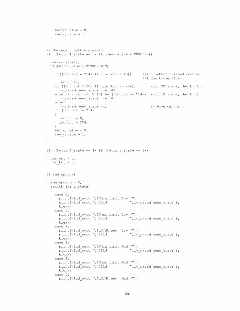
188
button_slow = 0; run_update = 1; // Decrement button pressed if ((button4_state == 0) && (menu_state < MENULEN)) button_slow++; if(button_slow > BUTTON_LIM) if((inc_but = 254) && (inc_cnt < 40)) //inc button pressed counter //& don't overflow inc_cnt++; if ((inc_cnt > 20) && (inc_but == 254)) //if 20 steps, dec by 100 iv_param[menu_state] -= 100; else if ((inc_cnt > 10) && (inc_but == 254)) //if 10 steps, dec by 10 iv_param[menu_state] -= 10; else iv_param[menu_state]--; // else dec by 1 if (inc_but != 254) inc_cnt = 0; inc_but = 254; button_slow = 0; run_update = 1; if ((button4_state == 1) && (button3_state == 1)) inc_cnt = 0; inc_but = 0; if(run_update) run_update = 0; switch (menu_state) case 0: printf(lcd_putc,"\fVmin limit Low "); printf(lcd_putc,"\n%5ld >",iv_param[menu_state]); break; case 1: printf(lcd_putc,"\fVmax limit Low <"); printf(lcd_putc,"\n%5ld >",iv_param[menu_state]); break; case 2: printf(lcd_putc,"\fdV/dt neg Low <"); printf(lcd_putc,"\n%5ld >",iv_param[menu_state]); break; case 3: printf(lcd_putc,"\fVmin limit Med <"); printf(lcd_putc,"\n%5ld >",iv_param[menu_state]); break; case 4: printf(lcd_putc,"\fVmax limit Med <"); printf(lcd_putc,"\n%5ld >",iv_param[menu_state]); break; case 5: printf(lcd_putc,"\fdV/dt neg Med <");
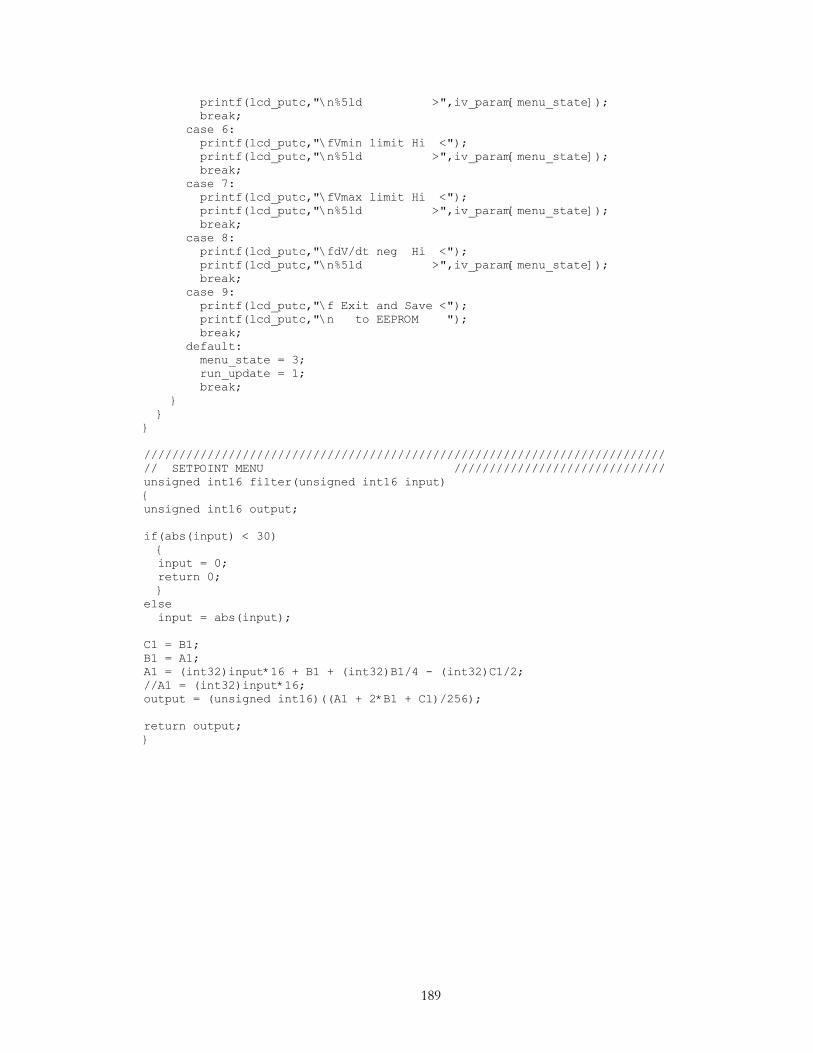
189
printf(lcd_putc,"\n%5ld >",iv_param[menu_state]); break; case 6: printf(lcd_putc,"\fVmin limit Hi <"); printf(lcd_putc,"\n%5ld >",iv_param[menu_state]); break; case 7: printf(lcd_putc,"\fVmax limit Hi <"); printf(lcd_putc,"\n%5ld >",iv_param[menu_state]); break; case 8: printf(lcd_putc,"\fdV/dt neg Hi <"); printf(lcd_putc,"\n%5ld >",iv_param[menu_state]); break; case 9: printf(lcd_putc,"\f Exit and Save <"); printf(lcd_putc,"\n to EEPROM "); break; default: menu_state = 3; run_update = 1; break; ////////////////////////////////////////////////////////////////////////// // SETPOINT MENU ////////////////////////////// unsigned int16 filter(unsigned int16 input) unsigned int16 output; if(abs(input) < 30) input = 0; return 0; else input = abs(input); C1 = B1; B1 = A1; A1 = (int32)input*16 + B1 + (int32)B1/4 - (int32)C1/2; //A1 = (int32)input*16; output = (unsigned int16)((A1 + 2*B1 + C1)/256); return output;

190
A.3.2 LCD driver subroutines
/////////////////////////////////////////////////////////////////////////// //// LCD_RSB.C //// //// Driver for common LCD modules //// //// //// //// lcd_init() Must be called before any other function. //// //// //// //// lcd_putc(c) Will display c on the next position of the LCD. //// //// The following have special meaning: //// //// \f Clear display //// //// \n Go to start of second line //// //// \b Move back one position //// //// //// //// lcd_gotoxy(x,y) Set write position on LCD (upper left is 1,1) //// //// //// //// lcd_getc(x,y) Returns character at position x,y on LCD //// /////////////////////////////////////////////////////////////////////////// //// LCD pin connections on PORT D: //// //// D0 Enable D4 D4 //// //// D1 RS D5 D5 //// //// D2 R/W D6 D6 //// //// D3 N/C D7 D7 //// /////////////////////////////////////////////////////////////////////////// //// (C) Copyright 2004 Robert S. Balog Jr. //// /////////////////////////////////////////////////////////////////////////// //// Revision history //// //// 8/29/2004 Detects series PIC based on CCS compiler definition //// //// to map correct memory addresses for I/O ports //// /////////////////////////////////////////////////////////////////////////// struct lcd_pin_map // This structure is overlayed int1 enable; // on to an I/O port to gain int1 rs; // access to the LCD pins. int1 rw; // The bits are allocated from int1 unused; // low order up. ENABLE will int data : 4; // be pin 0. lcd; #if defined(__PCH__) //Port memory addresses for series PIC #byte lcd = 0xF83 // port D for 18F series #else #byte lcd = 8 // port D for 16F series #endif #define set_tris_lcd(x) set_tris_d(x) #define lcd_type 2 // 0=5x7, 1=5x10, 2=2 lines #define lcd_line_two 0x40 // LCD RAM address for the second line //These bytes need to be sent to the LCD to start it up. BYTE const LCD_INIT_STRING[4] = 0x20 | (lcd_type << 2), 0xc, 1, 6; //The following are used for setting the I/O port direction register. struct lcd_pin_map const LCD_WRITE = 0,0,0,0,0; //Write mode, pins are out struct lcd_pin_map const LCD_READ = 0,0,0,0,15; //Read mode, data pins are in BYTE lcd_read_byte() BYTE low,high; set_tris_lcd(LCD_READ); lcd.rw = 1; delay_cycles(1); lcd.enable = 1; delay_cycles(1);
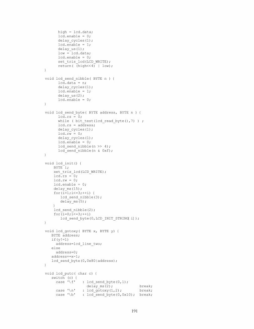
191
high = lcd.data; lcd.enable = 0; delay_cycles(1); lcd.enable = 1; delay_us(1); low = lcd.data; lcd.enable = 0; set_tris_lcd(LCD_WRITE); return( (high<<4) | low); void lcd_send_nibble( BYTE n ) lcd.data = n; delay_cycles(1); lcd.enable = 1; delay_us(2); lcd.enable = 0; void lcd_send_byte( BYTE address, BYTE n ) lcd.rs = 0; while ( bit_test(lcd_read_byte(),7) ) ; lcd.rs = address; delay_cycles(1); lcd.rw = 0; delay_cycles(1); lcd.enable = 0; lcd_send_nibble(n >> 4); lcd_send_nibble(n & 0xf); void lcd_init() BYTE i; set_tris_lcd(LCD_WRITE); lcd.rs = 0; lcd.rw = 0; lcd.enable = 0; delay_ms(15); for(i=1;i<=3;++i) lcd_send_nibble(3); delay_ms(5); lcd_send_nibble(2); for(i=0;i<=3;++i) lcd_send_byte(0,LCD_INIT_STRING[i]); void lcd_gotoxy( BYTE x, BYTE y) BYTE address; if(y!=1) address=lcd_line_two; else address=0; address+=x-1; lcd_send_byte(0,0x80|address); void lcd_putc( char c) switch (c) case '\f' : lcd_send_byte(0,1); delay_ms(2); break; case '\n' : lcd_gotoxy(1,2); break; case '\b' : lcd_send_byte(0,0x10); break;

192
default : lcd_send_byte(1,c); break; char lcd_getc( BYTE x, BYTE y) char value; lcd_gotoxy(x,y); while ( bit_test(lcd_read_byte(),7) ); // wait until busy flag is low lcd.rs=1; value = lcd_read_byte(); lcd.rs=0; return(value);

193
APPENDIX B MATLAB POWER FLOW SEARCH ALGORITHM
%***********************************************************************% % system_loadflow_v3.m % % Computes LoadFlow for EPNES (PhD Dissertation) DC System % % Uses experimentally obtained converter efficiency curves to % % enhance the loadflow accuracy. The algorithm initially assumes all % % node voltages to be equal to the open circuit source voltage. % % These voltages are used to obtain converter efficiency which is % % used to obtain the input power for each converter. The loadflow % % algorithm is then run. After the system voltages are obtained % % the converter efficiencies are updated and the loadflow iterated % % % % bus= col 1 bus number % % col 2 voltage p.u. % % col 3 angle % % col 4 P generation % % col 5 Q generation % % col 6 P load % % col 7 Q load % % col 8 G shunt % % col 9 B shunt % % col 10 bus type (1=swing, 3=load) % % % % line= col 1 fron bus % % col 2 to bus % % col 3 resistance p.u. % % col 4 reactance p.u. % % col 5 line charging p.u. % % % % v3 includes the system data in the datafile. It is not compatible % % with v2 datafiles % % % % Copyright 2005 Robert S. Balog Jr. % %***********************************************************************% clear all clc curvedatafile='buck_efficiency_curvefit.mat'; if exist(curvedatafile)==2 load(curvedatafile,'fit_*') %Load efficiency curve data for
converter else head=sprintf('Select file with efficiency curvefit data:'); [curvedatafile, curvedatapath] = uigetfile('*_efficiency_curvefit.mat',head); %Check if the user pressed cancel on the dialog. if isequal(curvedatafile,0) || isequal(curvedatapath,0) disp('No file loaded') else disp(['Curve fit data: ',curvedatafile]) end olddir=pwd; cd(curvedatapath) load(curvedatafile); cd(olddir) end loop_display=0; %display results through each iteration %%

194
%***Load experimental data file************************************** datafile=1; datapath=1; head=sprintf('Select experimental datafile to open (click cancel to quit)'); [datafile, datapath] = uigetfile('*_experimental_loadflow_data.m',head); %Check if the user pressed cancel on the dialog. if isequal(datafile,0) || isequal(datapath,0) disp('Experimental data: No file loaded') else disp(['Experimental data: ',datafile]) olddir=pwd; cd(datapath) run(datafile(1:end-2)); cd(olddir) end %*** SETUP STUDY *******************************************************% c=clock; if (c(4)>=12) tod='pm'; else tod='am'; end pathname=['Loadflow_',date,'@',num2str(mod(c(4),25),'%02g'),'-
',num2str(c(5),'%02g')]; filename=['data_',date,'@',num2str(mod(c(4),25),'%02g'),'-
',num2str(c(5),'%02g'),'.txt']; oldpath=pwd; %current directory mkdir(pathname); cd(pathname); diary(filename); disp('System Loadflow Contingency Analysis') disp(sprintf('Date of study: %s',[date,'@',num2str(mod(c(4),25),'%02g'),'-
',num2str(c(5),'%02g')])) disp(['Datafile: ',datafile]) %% %***SETUP parameters************************************************ Rbase=Vbase^2/Pbase; bus=[... 10, 3, Rs/Rbase, 0, 0; 3, 4 R34/Rbase, 0, 0; 4, 5 R45/Rbase, 0, 0;]; %% %loadflow parameters tol=1e-3; max_iterat=50; for trial=1:size(Po,1) %loop for each contingency disp(sprintf('\nContingency %g',trial)) %initialization error=1e-3; loop=1; loop_cnt=0; eff=ones(1,size(Po,2)); weighted_P=(Po(trial,3:5)-10)./(43-10); %eff(3:5)=fit_5V20W(Vbase); eff(3:5)=fit_5V18W(Vbase)*(1-weighted_P)+fit_5V43W(Vbase)*(weighted_P); VNODE(1,:)=ones(1,3)*Vbase; EFF(1,:)=eff; %loops through loadflow while adjusting converter efficiency while loop==1 loop_cnt=loop_cnt+1; loop_cnt;
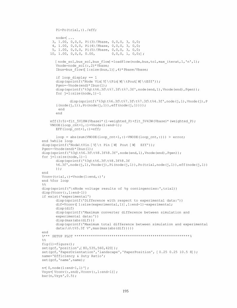
195
Pi=Po(trial,:)./eff; node=[... 3, 1.00, 0,0,0, Pi(3)/Pbase, 0,0,0, 3, 0,0; 4, 1.00, 0,0,0, Pi(4)/Pbase, 0,0,0, 3, 0,0; 5, 1.00, 0,0,0, Pi(5)/Pbase, 0,0,0, 3, 0,0; 10, 1.00, 0,0,0, 0.00, 0,0,0, 1, 0,0;]; [node_sol,bus_sol,bus_flow]=loadflow(node,bus,tol,max_iterat,1,'n',1); Vnode=node_sol(:,2)*Vbase; Ibus=bus_flow([1:size(bus,1)],4)*Pbase/Vbase; if loop_display == 1 disp(sprintf('Node Vin[V]\tPin[W]\tPout[W]\tEff')); Pgen=-Vnode(end)*Ibus(1); disp(sprintf('%3g\t%6.3f\t%7.3f\t%7.3f',node(end,1),Vnode(end),Pgen)); for j=1:size(node,1)-1
disp(sprintf('%3g\t%6.3f\t%7.3f\t%7.3f\t%4.3f',node(j,1),Vnode(j),Pi(node(j,1)),Po(node(j,1)),eff(node(j,1))));
end end eff(3:5)=fit_5V18W(Vbase)*(1-weighted_P)+fit_5V43W(Vbase)*(weighted_P); VNODE(loop_cnt+1,:)=Vnode(1:end-1); EFF(loop_cnt+1,:)=eff; loop = abs(sum(VNODE(loop_cnt+1,:)-VNODE(loop_cnt,:))) > error; end %while loop disp(sprintf('Node\tVin [V]\t Pin [W] Pout [W] Eff')); Pgen=-Vnode(end)*Ibus(1); disp(sprintf('%3g\t%6.3f\t%8.3f%8.3f',node(end,1),Vnode(end),Pgen)); for j=1:size(node,1)-1 disp(sprintf('%3g\t%6.3f\t%8.3f%8.3f
%6.3f',node(j,1),Vnode(j),Pi(node(j,1)),Po(trial,node(j,1)),eff(node(j,1))));
end Vconv(trial,:)=Vnode(1:end,:)'; end %for loop %% disp(sprintf('\nNode voltage results of %g contingencies:',trial)) disp(Vconv(:,1:end-1)) if exist('experimental') disp(sprintf('Difference with respect to experimental data:')) dif=Vconv([1:size(experimental,1)],1:end-1)-experimental; disp(dif) disp(sprintf('Maximum converter difference between simulation and
experimental data:')) disp(max(abs(dif))) disp(sprintf('Maximum total difference between simulation and experimental
data:\n\t%5.3f V',max(max(abs(dif))))) end %*** SETUP PLOT ********************************************************% %% fig(1)=figure(); set(gcf,'position',[80,535,560,420]); set(gcf,'PaperOrientation','landscape','PaperPosition', [0.25 0.25 10.5 8]); name='Efficiency & Duty Ratio'; set(gcf,'name',name); n=[0,node(1:end-1,1)']; Vsys=[Vconv(:,end),Vconv(:,1:end-1)]; bar(n,Vsys',0.5);
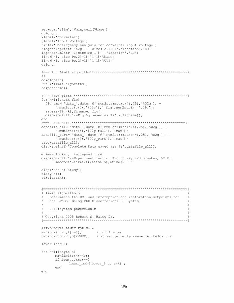
196
set(gca,'ylim',[Vmin,ceil(Vbase)]) grid on; xlabel('Converter') ylabel('Input Voltage') title('Contingency analysis for converter input voltage') %legend(sprintf('%2g',[1:size(Po,1)])','location','EO') legend(num2str([1:size(Po,1)]'),'location','EO') line([-1, size(Po,2)+1],[1,1]*Vbase) line([-1, size(Po,2)+1],[1,1]*VUVP) grid on %*** Run Limit algorithm************************************************% %% cd(oldpath) run ('limit_algorithm') cd(pathname); %*** Save plots ********************************************************% for k=1:length(fig) figname=['data_',date,'@',num2str(mod(c(4),25),'%02g'),'-
',num2str(c(5),'%02g'),'_fig',num2str(k),'.fig']; saveas(fig(k),figname,'fig'); disp(sprintf('\nFig %g saved as %s',k,figname)); end %*** Save data ********************************************************% datafile_all=['data_',date,'@',num2str(mod(c(4),25),'%02g'),'-
',num2str(c(5),'%02g_full'),'.mat']; datafile_part=['data_',date,'@',num2str(mod(c(4),25),'%02g'),'-
',num2str(c(5),'%02g_part'),'.mat']; save(datafile_all); disp(sprintf('Complete Data saved as: %s',datafile_all)); etime=clock-c; %ellapsed time disp(sprintf('\nExperiment ran for %2d hours, %2d minutes, %2.0f
seconds',etime(4),etime(5),etime(6))); disp('End of Study') diary off; cd(oldpath);
%***********************************************************************% % limit_algorithm.m % % Determines the UV load interuption and restoration setpoints for % % the EPNES (Balog PhD Dissertation) DC System % % % % USES:system_powerflow.m % % % % Copyright 2005 Robert S. Balog Jr. % %***********************************************************************% %FIND LOWER LIMIT FOR Vmin a=find(ind(:,4)~=1); %conv 4 = on b=find(Vconv(:,3)<VUVP); %highest priority converter below UVP lower_ind=[]; for k=1:length(a) ma=find(a(k)==b); if isempty(ma)==0 lower_ind=[lower_ind, a(k)]; end end
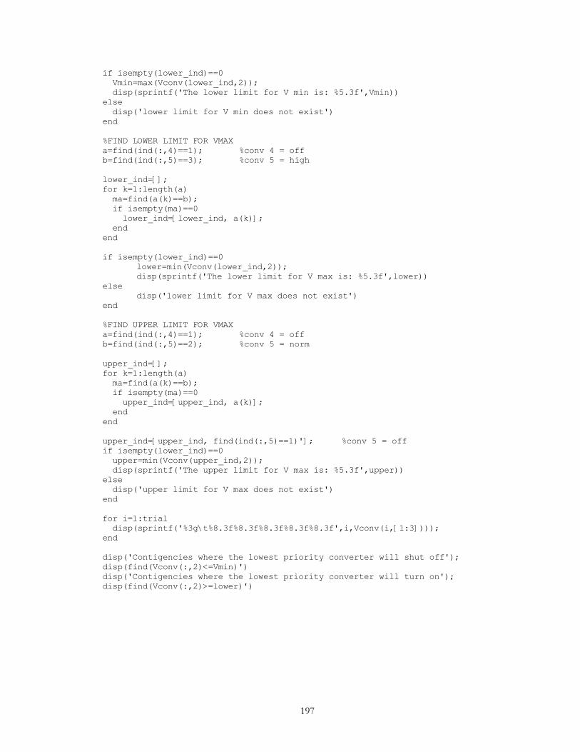
197
if isempty(lower_ind)==0 Vmin=max(Vconv(lower_ind,2)); disp(sprintf('The lower limit for V min is: %5.3f',Vmin)) else disp('lower limit for V min does not exist') end %FIND LOWER LIMIT FOR VMAX a=find(ind(:,4)==1); %conv 4 = off b=find(ind(:,5)==3); %conv 5 = high lower_ind=[]; for k=1:length(a) ma=find(a(k)==b); if isempty(ma)==0 lower_ind=[lower_ind, a(k)]; end end if isempty(lower_ind)==0 lower=min(Vconv(lower_ind,2)); disp(sprintf('The lower limit for V max is: %5.3f',lower)) else disp('lower limit for V max does not exist') end %FIND UPPER LIMIT FOR VMAX a=find(ind(:,4)==1); %conv 4 = off b=find(ind(:,5)==2); %conv 5 = norm upper_ind=[]; for k=1:length(a) ma=find(a(k)==b); if isempty(ma)==0 upper_ind=[upper_ind, a(k)]; end end upper_ind=[upper_ind, find(ind(:,5)==1)']; %conv 5 = off if isempty(lower_ind)==0 upper=min(Vconv(upper_ind,2)); disp(sprintf('The upper limit for V max is: %5.3f',upper)) else disp('upper limit for V max does not exist') end for i=1:trial disp(sprintf('%3g\t%8.3f%8.3f%8.3f%8.3f%8.3f',i,Vconv(i,[1:3]))); end disp('Contigencies where the lowest priority converter will shut off'); disp(find(Vconv(:,2)<=Vmin)') disp('Contigencies where the lowest priority converter will turn on'); disp(find(Vconv(:,2)>=lower)')

198
CURRICULUM VITA
Education:
Ph.D. in Electrical Engineering, May 2006 University of Illinois at Urbana-Champaign
Research Area: Power Electronics Thesis: “Autonomous Local Control in Distributed DC Power Systems” Advisor: Philip T. Krein Funding: NSF / ONR EPNES Grant No. ECS-0224839 M.S. in Electrical Engineering, May 2002 University of Illinois at Urbana-Champaign
Research Area: Power Electronics Thesis: “Coupled Inductor: A Basic Filter Building Block Analysis,
Simulation, and Examples” Advisor: Philip T. Krein B.S. in Electrical Engineering, May 1996 Rutgers University, College of Engineering, New Brunswick, NJ
Senior Thesis: “Topics in DSP: Interpolation, Decimation, and Delta-Sigma Quantization”
Advisor: Sophocles Orfanidis
Professional Experience:
University of Illinois at Urbana-Champaign Graduate Research Assistant, August 1999–2006
• Perform thesis related research and coursework • TA for Power Electronics Lab ECE369 • Nominated for the Harold L. Olesen Award for Excellence in Undergraduate
Teaching by Graduate Students • Prepare technical papers on numerous research topics (partial list available on web
page) • Apply industry design experience to improve experimental facilities • Update teaching lab with custom designed equipment, improvements to
instruction • Hire, supervise, and mentor undergraduate lab assistants
Lutron Electronics, Inc. Coopersburg, Pa, June 1996–July 1999
Project Electrical Engineer, June 1996–July 1999 • Analog and digital hardware design • Worst-case and failure analysis

199
• Product testing and quality assurance • Engineering support for manufacturing / operations at manufacturing facility in
Puerto Rico • Product development team leader • Product specification and definition • UL, FCC, CE, VDE compliance testing including European EMC directive • PCB design for EMC compatibility • Market research for new products • Mentor new engineers
Recruitment Manager, Rutgers University Campus, May 1998–July 1999 • Plan and manage all on-campus recruiting activities • Prescreen and interview candidates on-campus • Develop relationships with key faculty including plant visits and invited lectures • Increase company profile on campus by sponsoring student projects and activities
Career Explorer Post Advisor (volunteer), 1997–July 1999 • Promote Explorer Post program to high school students • Plan and coordinate technical program • Enlist company volunteers to prepare and present demonstration projects
Teaching Experience:
Power Electronics Laboratory, TA 2 semesters
Senior Design technical consultant, ongoing
Interests: Power Electronics, Power Systems, Electronics, Analog Circuits, Engineering, Analog Signal Processing, Digital Signal Processing
Patents:
R. S. Balog and P. T. Krein, "Commutation Technique for an AC-to-AC Converter Based on State Machine Control," US Patent application no. 11/202,597, filed 8/11/2005.
S. P. Sinha and R. S. Balog, "Lighting Control System for Different Load Types," US Patent 6 188 181, Feb. 13, 2001.
Professional Registration:
Professional Engineer, Illinois license no. 062-057093
Journal Papers:
R. S. Balog and P. T. Krein, "Commutation technique for high-frequency link cycloconverter," IEEE Power Electronics Letters, vol. 3, no. 3, pp. 101-104, Sept. 2005.
R. S. Balog et al., "Modern laboratory-based education for power electronics and electric machines," IEEE Transactions on Power Systems, vol. 20, no. 2, pp. 538-547, May 2005.

200
P. T. Krein, R. S. Balog, and G. Xin, "High-frequency link inverter for fuel cells based on multiple-carrier PWM," IEEE Transactions on Power Electronics, vol. 19, no. 5, pp. 1279-1288, Sept. 2004.
Conference Papers:
R. S. Balog, W. W. Weaver, and P. T. Krein, "The load as an energy asset in a distributed architecture," in IEEE Electric Ship Technologies Symposium, July 2005, pp. 261-267.
R. S. Balog, et al., "Blue-box approach to power electronics and machines educational laboratories," in IEEE Power Engineering Society General Meeting, 2005, pp. 962-970.
R. Balog and P. T. Krein, "A modular power electronics instructional laboratory," in Record, IEEE Power Electronics Specialist Conference, vol. 2, 2003, pp. 932-937.
P. T. Krein, X. Geng, and R. Balog, "High-frequency link inverter based on multiple-carrier PWM," in Proceedings, IEEE Applied Power Electronics Conference, vol. 2, 2002, pp. 997-1003.
P. T. Krein and R. Balog, "Low cost inverter sSuitable for medium-power fuel cell sources," in Record, IEEE Power Electronics Specialists Conference, vol. 1, 2002, pp. 321-326.
R. Balog and P. T. Krein, "Automatic tuning of coupled inductor filters," in Record, IEEE Power Electronics Specialists Conference, vol. 2, 2002, pp. 591-596.
P. T. Krein and R. S. Balog, "Life extension through charge equalization of lead-acid batteries," in Proceedings, IEEE International Telecommunications Energy Conference, 2002, pp. 516-523.
R. Balog, P. T. Krein, and D. C. Hamill, "Coupled inductors: A basic filter building block," in Proceedings, Electrical Manufacturing Coil Winding Association, 2000, pp. 271-278.
Magazine / Newsletter Articles:
R. S. Balog and J. W. Kimball, "Printed circuit board design for power electronics," to appear in IEEE Power Electronics Society Newsletter. R. Balog, P. T. Krein, and D. C. Hamill, "Coupled inductors: A basic filter building block," Electrical Manufacturing Coil Winding Association News, Winter 2002.
Technical Reports:
R. S. Balog, W. W. Weaver, and P. T. Krein, "Control strategies to use the load as a dynamic energy asset in a distributed architecture," EPNES Grantees Workshop, Dec. 2005.
R. S. Balog et al., "'Blue box' power electronics control modules for laboratory-based education," University of Illinois at Urbana-Champaign, Technical Report CEME-TR-2004-02, Jun. 2004.
R. S. Balog, "Coupled inductor: A basic filter building block analysis, simulation, and examples," University of Illinois at Urbana-Champaign, Technical Report CEME-TR-2002-1, Apr. 2002.

201
P. T. Krein, R. S. Balog, et al., "Low-cost 10 KW inverter system for fuel cell interfacing based on PWM cycloconverter," University of Illinois at Urbana-Champaign, Technical Report CEME-TR-01-3, Aug. 2001.
Selected Seminars and White Papers:
Printed Circuit Board (PCB) Overview and Design Issues
How to Keep Your Cool While Working with Power Electronics: Static Thermal Design Issues
Audio Pulse Width Modulation (PWM) Amplifier
Coupled Inductor Filters and Dynamic Stability Issues in Telecom DC Power Systems
Non-linear control techniques for a boost converter: Boundary Control
Grants and Contracts:
US Army Engineer Research and Development Center – Construction Engineering Research Laboratory (ERDC-CERL), Contract # W9132T-05-C-0026, “Advanced Energy Initiative ATO,” 9/2005–5/2006.
Professional Service:
Reviewer for:
IEEE Transitions on Power Electronics IEEE Power Electronics Letters IEEE Power Electronics Specialist conference (PESC) IEEE Applied Power Electronics Conference (APEC) IEEE Industry Applications Conference (IAS)
Affiliations:
Institute of Electrical & Electronics Engineers, Inc. (IEEE), member since 1992 Societies: Power Electronics, Power Engineering, Industrial Applications, Circuits and Systems
American Society for Engineering Education (ASEE)
National Society of Professional Engineers (NSPE)
Illinois Society of Professional Engineers (ISPE)
Eta Kappa Nu (HKN) - Electrical Engineering Honor Society
Electrical Manufacturing Coil Winding Association (EMCWA)
Kappa Delta Rho National Fraternity
National Eagle Scout Association, Boy Scouts of America
Awards:
Grainger Outstanding Power Engineering Award, 2006
Harriett & Robert Perry Fellow, 2005–2006
Ernest A. Reid Fellow, 2004–2005

202
IEEE International Telecommunications Energy Conference (INTELEC) Fellow, 2001–2002.
EMCWA Scholarship, 2001
Grainger Outstanding Power Engineering Award, 2001