Embed Size (px)
Citation preview

9,$ 7HFKQRORJLHV
!"!#$%&
'("&%#!&$)&#*+$, ,-,!"$#.,
"&%#!&$)"$ !&#$#&)"$!/!)$,
) #!$!00-11!&#$&&$&"# &#,
)"# &#,2&3!#$"# &#,#,
$#)&$$!,&#! #4, )%!"$ !3,
!,&"(!"&$'&#!"!%&&",),!"$
&&#!)#&, !%&,!"$+!"&&$"#"%
# 567-
!/,11-
!&(" %&,"7
8"9 : &RS\ULJKW 9,$ 7HFKQRORJLHV ,QFRUSRUDWHG 3ULQWHG LQ WKH 8QLWHG 6WDWHV $// 5,*+76 5(6(59('
1R SDUW RI WKLV GRFXPHQW PD\ EH UHSURGXFHG WUDQVPLWWHG WUDQVFULEHG VWRUHG LQ D UHWULHYDO V\VWHP RU WUDQVODWHG LQWRDQ\ ODQJXDJH LQ DQ\ IRUP RU E\ DQ\ PHDQV HOHFWURQLF PHFKDQLFDO PDJQHWLF RSWLFDO FKHPLFDO PDQXDO RU RWKHUZLVHZLWKRXW WKH SULRU ZULWWHQ SHUPLVVLRQ RI 9,$ 7HFKQRORJLHV ,QFRUSRUDWHG
97&$ 97&% DQG 6XSHU 6RXWK PD\ RQO\ EH XVHG WR LGHQWLI\ SURGXFWV RI 9,$ 7HFKQRORJLHV ,QF
LD D UHJLVWHUHG WUDGHPDUN RI 9,$ 7HFKQRORJLHV ,QFRUSRUDWHG3670 LV D UHJLVWHUHG WUDGHPDUN RI ,QWHUQDWLRQDO %XVLQHVV 0DFKLQHV &RUS3HQWLXP70 3HQWLXP3UR70 3HQWLXP,,70 3HQWLXP,,,70 &HOHURQ70DQG *7/70 DUH UHJLVWHUHG WUDGHPDUNV RI ,QWHO &RUS:LQGRZV 70 :LQGRZV 70 :LQGRZV 1770 DQG 3OXJ DQG 3OD\70 DUH UHJLVWHUHG WUDGHPDUNV RI 0LFURVRIW &RUS3&,70 LV D UHJLVWHUHG WUDGHPDUN RI WKH 3&, 6SHFLDO ,QWHUHVW *URXS$OO WUDGHPDUNV DUH WKH SURSHUWLHV RI WKHLU UHVSHFWLYH RZQHUV
$69; "9 : 1R OLFHQVH LV JUDQWHG LPSOLHG RU RWKHUZLVH XQGHU DQ\ SDWHQW RU SDWHQW ULJKWV RI 9,$ 7HFKQRORJLHV 9,$ 7HFKQRORJLHVPDNHV QR ZDUUDQWLHV LPSOLHG RU RWKHUZLVH LQ UHJDUG WR WKLV GRFXPHQW DQG WR WKH SURGXFWV GHVFULEHG LQ WKLV GRFXPHQW7KH LQIRUPDWLRQ SURYLGHG E\ WKLV GRFXPHQW LV EHOLHYHG WR EH DFFXUDWH DQG UHOLDEOH WR WKH SXEOLFDWLRQ GDWH RI WKLVGRFXPHQW +RZHYHU 9,$ 7HFKQRORJLHV DVVXPHV QR UHVSRQVLELOLW\ IRU DQ\ HUURUV LQ WKLV GRFXPHQW )XUWKHUPRUH 9,$7HFKQRORJLHV DVVXPHV QR UHVSRQVLELOLW\ IRU WKH XVH RU PLVXVH RI WKH LQIRUPDWLRQ LQ WKLV GRFXPHQW DQG IRU DQ\ SDWHQWLQIULQJHPHQWV WKDW PD\ DULVH IURP WKH XVH RI WKLV GRFXPHQW 7KH LQIRUPDWLRQ DQG SURGXFW VSHFLILFDWLRQV ZLWKLQ WKLVGRFXPHQW DUH VXEMHFW WR FKDQJH DW DQ\ WLPH ZLWKRXW QRWLFH DQG ZLWKRXW REOLJDWLRQ WR QRWLI\ DQ\ SHUVRQ RI VXFK FKDQJH <<9 6: 86$ 2IILFH 7DLSHL 2IILFH
0LVVLRQ &RXUW WK)ORRU 1R
)UHPRQW &$ &KXQJ&KHQJ 5RDG +VLQ7LHQ86$ 7DLSHL 7DLZDQ 52&7HO 7HO )D[ )D[
59 6:+RPH 3DJH http://www.via.com.tw ±RU http://www.viatech.com)73 6HUYHU ftp.via.com.tw%%6
VT82C686B
Revision 2.1 April 27, 2001 -i- Revision History
7HFKQRORJLHV ,QF'HOLYHULQJ 9DOXH'HOLYHULQJ 9DOXH
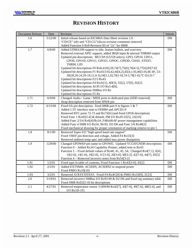
REVISION HISTORY
Document Release Date Revision Initials 1.6 5/22/00 Initial release based on 82C686A Data Sheet revision 1.6
“CD/CE” info and “CD-CG”silicon revision comments removed Added Function 0 Rx8 Revision ID of “2x” for 686B
DH
1.7 6/8/00 Added UDMA100 support to title, feature bullets, and overview Removed external APIC support, added IRQ0 input & internal THRM# output Updated pin descriptions: MCCS# (U5/U8 select), GPI3, GPI10, GPI11,
GPO6, GPO10, GPO11, GPO21, GPIOC, GPIOD, CHAS, ATEST, THRM, LID
Updated bit descriptions F0 Rx8,41[6],59,74[7],75[6],76[4-3],77[4],85[7-6] Updated bit descriptions F1 Rx41[3-0],42,44[4,2],45[4,1-0],46[5-0],4E-4F, 53-
50[28,26-24,20-19,12,4-3],54[5,1,0],70[1-0],74-5,78[1-0],7C-D,C0-7 Updated bit descriptions F2/3 Rx43 Updated bit descriptions F4 Rx41[1], 4D[3], 55[2], 57[0], D2[2] Updated bit descriptions ACPI I/O Rx5-4[8], Updated bit descriptions SMBus I/O Rx Updated bit descriptions F5 Rx
DH
1.71 6/9/00 Changed Audio / Game / MIDI ports to dedicated pins (SDD removed) Strap description removed from SPKR pin
DH
1.72 6/15/00 Fixed SA pin description; fixed 686B part # in figures 1 & 7 Added 1.5V interface note to FERR# and APCD1-0 Removed RTC ports 72-73 and Rx75[6] (and fixed GPO6 description) Fixed Func 1 Rx45[5-4] & default, PM I/O Rx20-25[5], 2A[10] Added Func 2/3/4 Rx6[4]/Rx34, F4Rx68-6F power management capabilities Added Func 4 SMB I/O Rx54, 90-93, D2-D6 and Func 5/6 Rx48[3] Fixed mechanical drawing for proper orientation of marking relative to pin 1
DH
1.8 8/1/00 Removed Super-I/O “high speed baud rate support” Fixed VREF pin direction and voltage, Added F4 Rx55[3] Removed ambient temp spec and added max power dissipation
DH
1.9 12/8/00 Changed GPOWE# pin name to GPOWE; Updated VCCH/GNDH descriptions Function 0 – Added Rx34 Capability Pointer, added note to Rx43 Function 1 – Fixed default values of Rx40, 41, 45, 54; Changed Rx4[7,1], 6[4],
10[2-0], 14[1-0], 18[2-0], 1C[1-0], 20[3-0], 40[3-2], 42[7-6], 44[7], 45[5] Function 4 – Removed incorrect notes from Rx54[3-2]
DH
1.91 1/2/01 Fixed typo in table of contents, Fixed Function 1 Rx43[3-0], 45[2] DH 1.92 2/2/01 Added EXTSMI#, ACSDIN, ACSDIN2 to suspend power
Fixed PMIO Rx10[10] DH
1.93 3/2/01 Removed ATEST/DTEST; Fixed F4 Rx4C[0] & PMIO Rx10[9], 2C[3] DH 2.0 3/19/01 Removed incorrect SMBus I/O Rx93-90 & D2-D6 and fixed reg summary table
Fixed SMB RxD2[1-0] bit descriptions DH
2.1 4/27/01 Removed temperature sensor 3 (HWM Rx42[7], 44[7-6], 49[7-6], 4B[5-4], and I/O Rx1D-1F)
DH
VT82C686B
Revision 2.1 April 27, 2001 -ii- Table of Contents
7HFKQRORJLHV ,QF'HOLYHULQJ 9DOXH'HOLYHULQJ 9DOXH
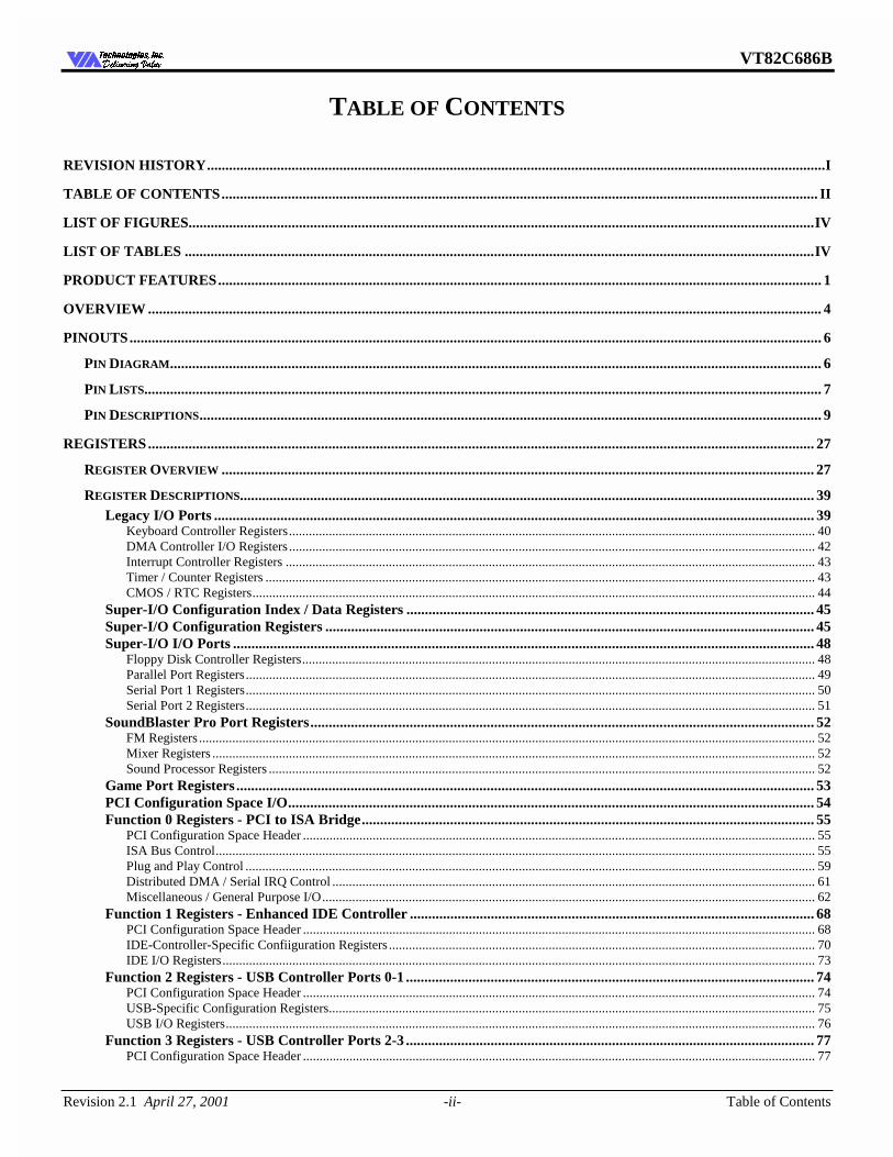
TABLE OF CONTENTS
REVISION HISTORY........................................................................................................................................................................I
TABLE OF CONTENTS.................................................................................................................................................................. II
LIST OF FIGURES..........................................................................................................................................................................IV
LIST OF TABLES ...........................................................................................................................................................................IV
PRODUCT FEATURES.................................................................................................................................................................... 1
OVERVIEW ....................................................................................................................................................................................... 4
PINOUTS............................................................................................................................................................................................ 6
PIN DIAGRAM................................................................................................................................................................................. 6
PIN LISTS........................................................................................................................................................................................ 7
PIN DESCRIPTIONS......................................................................................................................................................................... 9
REGISTERS..................................................................................................................................................................................... 27
REGISTER OVERVIEW ................................................................................................................................................................. 27
REGISTER DESCRIPTIONS............................................................................................................................................................ 39 Legacy I/O Ports ................................................................................................................................................................... 39
Keyboard Controller Registers.............................................................................................................................................................. 40 DMA Controller I/O Registers .............................................................................................................................................................. 42 Interrupt Controller Registers ............................................................................................................................................................... 43 Timer / Counter Registers ..................................................................................................................................................................... 43 CMOS / RTC Registers......................................................................................................................................................................... 44
Super-I/O Configuration Index / Data Registers ............................................................................................................... 45 Super-I/O Configuration Registers ..................................................................................................................................... 45 Super-I/O I/O Ports .............................................................................................................................................................. 48
Floppy Disk Controller Registers.......................................................................................................................................................... 48 Parallel Port Registers........................................................................................................................................................................... 49 Serial Port 1 Registers........................................................................................................................................................................... 50 Serial Port 2 Registers........................................................................................................................................................................... 51
SoundBlaster Pro Port Registers......................................................................................................................................... 52 FM Registers ......................................................................................................................................................................................... 52 Mixer Registers ..................................................................................................................................................................................... 52 Sound Processor Registers .................................................................................................................................................................... 52
Game Port Registers ............................................................................................................................................................. 53 PCI Configuration Space I/O............................................................................................................................................... 54 Function 0 Registers - PCI to ISA Bridge........................................................................................................................... 55
PCI Configuration Space Header .......................................................................................................................................................... 55 ISA Bus Control.................................................................................................................................................................................... 55 Plug and Play Control ........................................................................................................................................................................... 59 Distributed DMA / Serial IRQ Control ................................................................................................................................................. 61 Miscellaneous / General Purpose I/O.................................................................................................................................................... 62
Function 1 Registers - Enhanced IDE Controller .............................................................................................................. 68 PCI Configuration Space Header .......................................................................................................................................................... 68 IDE-Controller-Specific Confiiguration Registers ................................................................................................................................ 70 IDE I/O Registers.................................................................................................................................................................................. 73
Function 2 Registers - USB Controller Ports 0-1 ............................................................................................................... 74 PCI Configuration Space Header .......................................................................................................................................................... 74 USB-Specific Configuration Registers.................................................................................................................................................. 75 USB I/O Registers................................................................................................................................................................................. 76
Function 3 Registers - USB Controller Ports 2-3 ............................................................................................................... 77 PCI Configuration Space Header .......................................................................................................................................................... 77
VT82C686B
Revision 2.1 April 27, 2001 -iii- Table of Contents
7HFKQRORJLHV ,QF'HOLYHULQJ 9DOXH'HOLYHULQJ 9DOXH
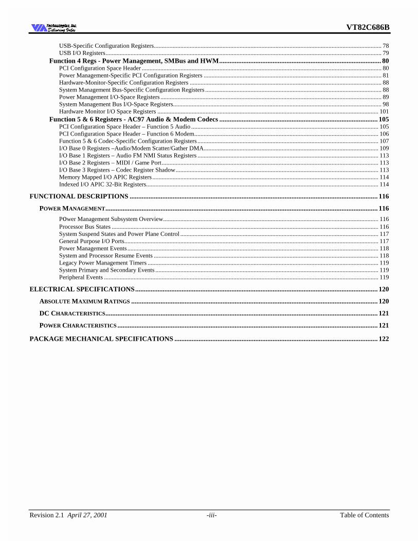
USB-Specific Configuration Registers.................................................................................................................................................. 78 USB I/O Registers................................................................................................................................................................................. 79
Function 4 Regs - Power Management, SMBus and HWM.............................................................................................. 80 PCI Configuration Space Header .......................................................................................................................................................... 80 Power Management-Specific PCI Configuration Registers .................................................................................................................. 81 Hardware-Monitor-Specific Configuration Registers ........................................................................................................................... 88 System Management Bus-Specific Configuration Registers ................................................................................................................. 88 Power Management I/O-Space Registers .............................................................................................................................................. 89 System Management Bus I/O-Space Registers...................................................................................................................................... 98 Hardware Monitor I/O Space Registers .............................................................................................................................................. 101
Function 5 & 6 Registers - AC97 Audio & Modem Codecs ............................................................................................ 105 PCI Configuration Space Header – Function 5 Audio ........................................................................................................................ 105 PCI Configuration Space Header – Function 6 Modem...................................................................................................................... 106 Function 5 & 6 Codec-Specific Configuration Registers .................................................................................................................... 107 I/O Base 0 Registers –Audio/Modem Scatter/Gather DMA................................................................................................................ 109 I/O Base 1 Registers – Audio FM NMI Status Registers .................................................................................................................... 113 I/O Base 2 Registers – MIDI / Game Port........................................................................................................................................... 113 I/O Base 3 Registers – Codec Register Shadow.................................................................................................................................. 113 Memory Mapped I/O APIC Registers ................................................................................................................................................. 114 Indexed I/O APIC 32-Bit Registers..................................................................................................................................................... 114
FUNCTIONAL DESCRIPTIONS ................................................................................................................................................ 116
POWER MANAGEMENT.............................................................................................................................................................. 116 Power Management Subsystem Overview.......................................................................................................................................... 116 Processor Bus States ........................................................................................................................................................................... 116 System Suspend States and Power Plane Control ............................................................................................................................... 117 General Purpose I/O Ports................................................................................................................................................................... 117 Power Management Events ................................................................................................................................................................. 118 System and Processor Resume Events ................................................................................................................................................ 118 Legacy Power Management Timers .................................................................................................................................................... 119 System Primary and Secondary Events ............................................................................................................................................... 119 Peripheral Events ................................................................................................................................................................................ 119
ELECTRICAL SPECIFICATIONS............................................................................................................................................. 120
ABSOLUTE MAXIMUM RATINGS ............................................................................................................................................... 120
DC CHARACTERISTICS.............................................................................................................................................................. 121
POWER CHARACTERISTICS ....................................................................................................................................................... 121
PACKAGE MECHANICAL SPECIFICATIONS ...................................................................................................................... 122
VT82C686B
Revision 2.1 April 27, 2001 -iv- Table of Contents
7HFKQRORJLHV ,QF'HOLYHULQJ 9DOXH'HOLYHULQJ 9DOXH
LIST OF FIGURES
FIGURE 1. PC SYSTEM CONFIGURATION USING THE VT82C686B ................................................................................. 5 FIGURE 2. VT82C686B BALL DIAGRAM (TOP VIEW)........................................................................................................... 6 FIGURE 3. VT82C686B PIN LIST (NUMERICAL ORDER)...................................................................................................... 7 FIGURE 4. VT82C686B PIN LIST (ALPHABETICAL ORDER)............................................................................................... 8 FIGURE 5. STRAP OPTION CIRCUIT....................................................................................................................................... 60 FIGURE 6. POWER MANAGEMENT SUBSYSTEM BLOCK DIAGRAM ......................................................................... 116 FIGURE 8. MECHANICAL SPECIFICATIONS – 352 PIN BALL GRID ARRAY PACKAGE......................................... 122
LIST OF TABLES
TABLE 1. PIN DESCRIPTIONS..................................................................................................................................................... 9 TABLE 2. SYSTEM I/O MAP ....................................................................................................................................................... 27 TABLE 3. REGISTERS.................................................................................................................................................................. 28 TABLE 4. KEYBOARD CONTROLLER COMMAND CODES .............................................................................................. 41 TABLE 5. CMOS REGISTER SUMMARY................................................................................................................................. 44
VT82C686B
Revision 2.1 April 27, 2001 -1- Product Features
7HFKQRORJLHV ,QF'HOLYHULQJ 9DOXH'HOLYHULQJ 9DOXH
VT82C686B PSIPC PCI SUPER-I/O INTEGRATED PERIPHERAL CONTROLLER
PC99 COMPLIANT PCI-TO-ISA BRIDGE WITH INTEGRATED SUPER-I/O (FDC, LPT, COM1/2, AND IR),
INTEGRATED HARDWARE SOUNDBLASTER/DIRECT SOUND AC97 AUDIO, ULTRADMA-33/66/100 MASTER MODE PCI-EIDE CONTROLLER,
USB CONTROLLER, KEYBOARD CONTROLLER, RTC, DISTRIBUTED DMA, SERIAL IRQ, PLUG AND PLAY,
ACPI, ENHANCED POWER MANAGEMENT, SMBUS, AND TEMPERATURE, VOLTAGE, AND FAN-SPEED MONITORING
PRODUCT FEATURES
• Inter-operable with VIA and other Host-to-PCI Bridges
− Combine with VT82C598 for a complete Super-7 (66/75/83/100MHz) PCI / AGP / ISA system (Apollo MVP3) − Combine with VT8501 for a complete Super-7 system with integrated 2D / 3D graphics (Apollo MVP4) − Combine with VT82C693 for a complete 66 / 100 / 133 MHz Socket-370 or Slot-1 system (Apollo Pro133) − Combine with VT8601 for a complete 66 / 100 / 133 MHz Socket-370 or Slot-1 system with integrated 2D / 3D
graphics (Apollo ProMedia) − Inter-operable with Intel or other Host-to-PCI bridges for a complete PC99 compliant PCI / AGP / ISA system
• PCI to ISA Bridge
− Integrated ISA Bus Controller with integrated DMA, timer, and interrupt controller − Integrated Keyboard Controller with PS2 mouse support − Integrated DS12885-style Real Time Clock with extended 256 byte CMOS RAM and Day/Month Alarm for ACPI − Integrated USB Controller with root hub and four function ports − Integrated UltraDMA-33/66/100 master mode EIDE controller with enhanced PCI bus commands − PCI-2.2 compliant with delay transaction and remote power management − Eight double-word line buffer between PCI and ISA bus − One level of PCI to ISA post-write buffer − Supports type F DMA transfers − Distributed DMA support for ISA legacy DMA across the PCI bus − Serial interrupt for docking and non-docking applications − Fast reset and Gate A20 operation − Edge trigger or level sensitive interrupt − Flash EPROM, 4Mb EPROM and combined BIOS support − Supports positive and subtractive decoding
VT82C686B
Revision 2.1 April 27, 2001 -2- Product Features
7HFKQRORJLHV ,QF'HOLYHULQJ 9DOXH'HOLYHULQJ 9DOXH
• UltraDMA-33 / 66 / 100 Master Mode PCI EIDE Controller
− Dual channel master mode PCI supporting four Enhanced IDE devices − Transfer rate up to 33MB/sec to cover PIO mode 4, multi-word DMA mode 2 drives, and UltraDMA-33 interface − Increased reliability using UltraDMA-66 transfer protocols − Increased performance using UltraDMA-100 mode 5 − Thirty-two levels (doublewords) of prefetch and write buffers − Dual DMA engine for concurrent dual channel operation − Bus master programming interface for SFF-8038I rev.1.0 and Windows-95 compliant − Full scatter gather capability − Support ATAPI compliant devices including DVD devices − Support PCI native and ATA compatibility modes − Complete software driver support
• Integrated Super IO Controller
− Supports 2 serial ports, IR port, parallel port, and floppy disk controller functions − Two UARTs for Complete Serial Ports Programmable character lengths (5,6,7,8) Even, odd, stick or no parity bit generation and detection Programmable baud rate generator Independent transmit/receiver FIFOs Modem Control Plug and play with 96 base IO address and 12 IRQ options − Infrared-IrDA (HPSIR) and ASK (Amplitude Shift Keyed) IR port multiplexed on COM2 − Multi-mode parallel port Standard mode, ECP and EPP support Plug and play with 192 base IO address, 12 IRQ and 4 DMA options − Floppy Disk Controller 16 bytes of FIFO Data rates up to 1Mbps Perpendicular recording driver support Two FDDs with drive swap support Plug and play with 48 base IO address, 12 IRQ and 4 DMA options
• SoundBlaster Pro Hardware and Direct Sound Ready AC97 Digital Audio Controller
− Dual full-duplex Direct Sound channels between system memory and AC97 link − PCI master interface with scatter / gather and bursting capability − 32 byte FIFO of each direct sound channel − Host based sample rate converter and mixer − Standard v1.0 or v2.0 AC97 Codec interface for single or cascaded AC97 Codec’s from multiple vendors − Loopback capability for re-directing mixed audio streams into USB and 1394 speakers − Hardware SoundBlaster Pro for Windows DOS box and real-mode DOS legacy compatibility − Plug and play with 4 IRQ, 4 DMA, and 4 I/O space options for SoundBlaster Pro and MIDI hardware − Hardware assisted FM synthesis for legacy compatibility − Direct two game ports and one MIDI port interface − Complete software driver support for Windows-95/98/2000 and Windows-NT
• Voltage, Temperature, Fan Speed Monitor and Controller
− Five positive voltage (one internal), three temperature (one internal) and two fan-speed monitoring − Programmable control, status, monitor and alarm for flexible desktop management − External thermister or internal bandgap temperature sensing − Automatic clock throttling with integrated temperature sensing − Internal core VCC voltage sensing − Flexible external voltage sensing arrangement (any positive supply and battery)
VT82C686B
Revision 2.1 April 27, 2001 -3- Product Features
7HFKQRORJLHV ,QF'HOLYHULQJ 9DOXH'HOLYHULQJ 9DOXH
• Universal Serial Bus Controller
− USB v.1.1 and Intel Universal HCI v.1.1 compatible − Eighteen level (doublewords) data FIFO with full scatter and gather capability − Root hub and four function ports − Integrated physical layer transceivers with optional over-current detection status on USB inputs − Legacy keyboard and PS/2 mouse support
• System Management Bus Interface
− Host interface for processor communications − Slave interface for external SMBus masters
• Sophisticated PC99-Compatible Mobile Power Management
− Supports both ACPI (Advanced Configuration and Power Interface) and legacy (APM) power management − ACPI v1.0 Compliant − APM v1.2 Compliant − CPU clock throttling and clock stop control for complete ACPI C0 to C3 state support − PCI bus clock run, Power Management Enable (PME) control, and PCI/CPU clock generator stop control − Supports multiple system suspend types: power-on suspends with flexible CPU/PCI bus reset options, suspend to DRAM, and suspend to disk (soft-off), all with hardware automatic wake-up − Multiple suspend power plane controls and suspend status indicators − One idle timer, one peripheral timer and one general purpose timer, plus 24/32-bit ACPI compliant timer − Normal, doze, sleep, suspend and conserve modes − Global and local device power control − System event monitoring with two event classes − Primary and secondary interrupt differentiation for individual channels − Dedicated input pins for power and sleep buttons, external modem ring indicator, and notebook lid open/close for
system wake-up − Up to 12 general purpose input ports and 23 output ports − Multiple internal and external SMI sources for flexible power management models − One programmable chip select and one microcontroller chip select − Enhanced integrated real time clock (RTC) with date alarm, month alarm, and century field − Thermal alarm on either external or any combination of three internal temperature sensing circuits − Hot docking support − I/O pad leakage control
• Plug and Play Controller
− PCI interrupts steerable to any interrupt channel − Steerable interrupts for integrated peripheral controllers: USB, floppy, serial, parallel, audio, soundblaster, MIDI − Steerable DMA channels for integrated floppy, parallel, and soundblaster pro controllers − One additional steerable interrupt channel for on-board plug and play devices − Microsoft Windows 98TM, Windows NTTM, Windows 95TM and plug and play BIOS compliant
• Integrated I/O APIC (Advanced Peripheral Interrupt Controller)
• Built-in NAND-tree pin scan test capability
• 0.35um, 3.3V, low power CMOS process
• Single chip 27x27 mm, 352 pin BGA
VT82C686B
Revision 2.1 April 27, 2001 -4- Overview
7HFKQRORJLHV ,QF'HOLYHULQJ 9DOXH'HOLYHULQJ 9DOXH
OVERVIEW
The VT82C686B PSIPC (PCI Super-I/O Integrated Peripheral Controller) is a high integration, high performance, power-efficient, and high compatibility device that supports Intel and non-Intel based processor to PCI bus bridge functionality to make a complete Microsoft PC99-compliant PCI/ISA system. In addition to complete ISA extension bus functionality, the VT82C686B includes standard intelligent peripheral controllers:
a) Master mode enhanced IDE controller with dual channel DMA engine and interlaced dual channel commands. Dedicated FIFO coupled with scatter and gather master mode operation allows high performance transfers between PCI and IDE devices. In addition to standard PIO and DMA mode operation, the VT82C686B also supports the UltraDMA-33 standard to allow reliable data transfer rates up to 33MB/sec throughput. The VT82C686B also supports the UltraDMA-66 and UltraDMA-100 (ATA-100) standards. The IDE controller is SFF-8038I v1.0 and Microsoft Windows-family compliant.
b) Universal Serial Bus controller that is USB v1.1 and Universal HCI v1.1 compliant. The VT82C686B includes the root hub with four function ports with integrated physical layer transceivers. The USB controller allows hot plug and play and isochronous peripherals to be inserted into the system with universal driver support. The controller also implements legacy keyboard and mouse support so that legacy software can run transparently in a non-USB-aware operating system environment.
c) Keyboard controller with PS2 mouse support.
d) Real Time Clock with 256 byte extended CMOS. In addition to the standard ISA RTC functionality, the integrated RTC also includes the date alarm, century field, and other enhancements for compatibility with the ACPI standard.
e) Notebook-class power management functionality compliant with ACPI and legacy APM requirements. Multiple sleep states (power-on suspend, suspend-to-DRAM, and suspend-to-Disk) are supported with hardware automatic wake-up. Additional functionality includes event monitoring, CPU clock throttling and stop (Intel processor protocol), PCI bus clock stop control, modular power, clock and leakage control, hardware-based and software-based event handling, general purpose I/O, chip select and external SMI.
f) Hardware monitoring subsystem for managing system / motherboard voltage levels, temperatures, and fan speeds
g) Full System Management Bus (SMBus) interface.
h) Two 16550-compatible serial I/O ports with infrared communications port option on the second port.
i) Integrated PCI-mastering dual full-duplex direct-sound AC97-link-compatible sound system. Hardware soundblaster-pro and hardware-assisted FM blocks are included for Windows DOS box and real-mode DOS compatibility. Loopback capability is also implemented for directing mixed audio streams into USB and 1394 speakers for high quality digital audio.
j) Two game ports and one MIDI port
k) ECP/EPP-capable parallel port
l) Standard floppy disk drive interface
m) Distributed DMA capability for support of ISA legacy DMA over the PCI bus. Serial IRQ is also supported for docking and non-docking applications.
n) Plug and Play controller that allows complete steerability of all PCI interrupts and internal interrupts / DMA channels to any interrupt channel. One additional steerable interrupt channel is provided to allow plug and play and reconfigurability of on-board peripherals for Windows family compliance.
o) Internal I/O APIC (Advanced Programmable Interrupt Controller)
VT82C686B
Revision 2.1 April 27, 2001 -5- Overview
7HFKQRORJLHV ,QF'HOLYHULQJ 9DOXH'HOLYHULQJ 9DOXH
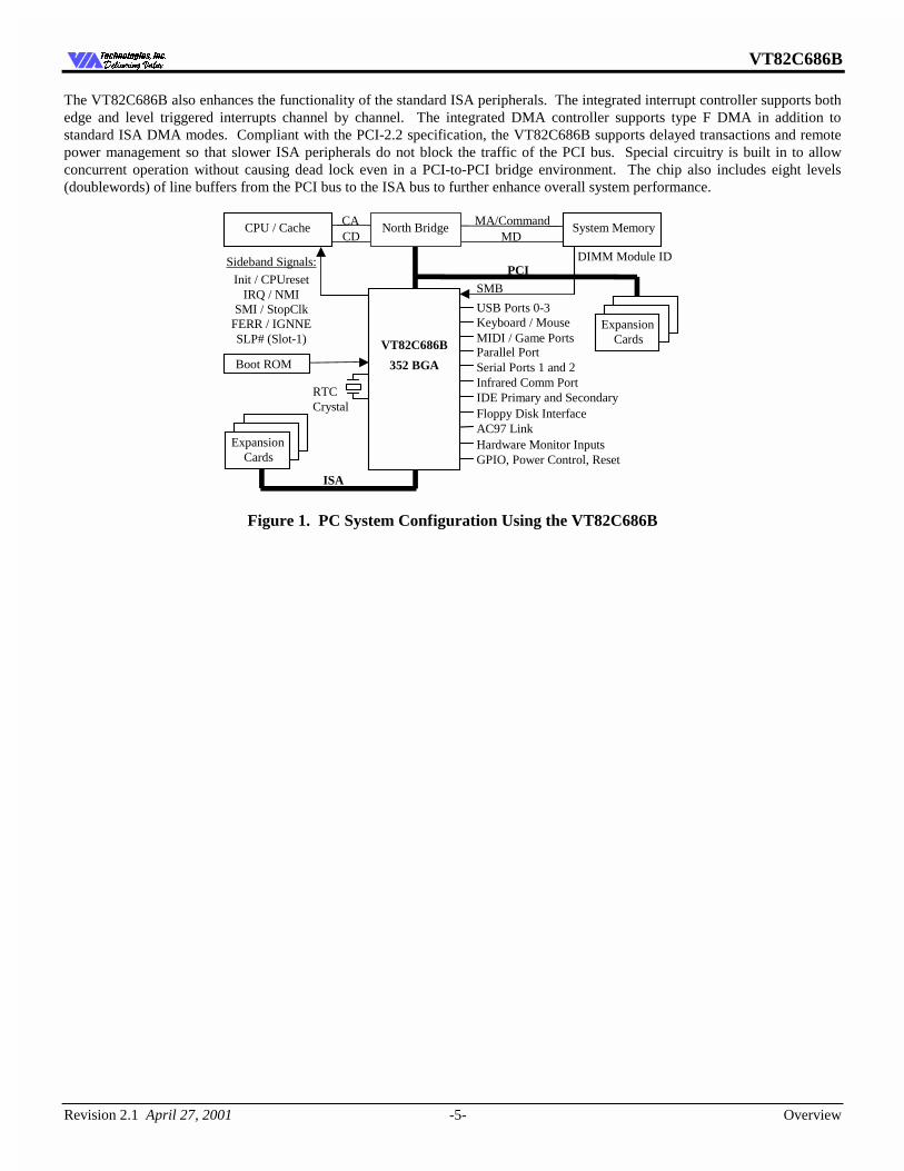
The VT82C686B also enhances the functionality of the standard ISA peripherals. The integrated interrupt controller supports both edge and level triggered interrupts channel by channel. The integrated DMA controller supports type F DMA in addition to standard ISA DMA modes. Compliant with the PCI-2.2 specification, the VT82C686B supports delayed transactions and remote power management so that slower ISA peripherals do not block the traffic of the PCI bus. Special circuitry is built in to allow concurrent operation without causing dead lock even in a PCI-to-PCI bridge environment. The chip also includes eight levels (doublewords) of line buffers from the PCI bus to the ISA bus to further enhance overall system performance.
CPU / CacheCA
PCI
MDMA/Command
CDNorth Bridge
352 BGA
VT82C686B
System Memory
Sideband Signals:
Init / CPUresetIRQ / NMI
SMI / StopClkFERR / IGNNESLP# (Slot-1)
USB Ports 0-3
Serial Ports 1 and 2
ISA
RTCCrystal
Boot ROM
ExpansionCards
Infrared Comm PortIDE Primary and SecondaryFloppy Disk InterfaceAC97 LinkHardware Monitor Inputs
Keyboard / Mouse
SMB
DIMM Module ID
ExpansionCards GPIO, Power Control, Reset
MIDI / Game PortsParallel Port
Figure 1. PC System Configuration Using the VT82C686B
VT82C686B
Revision 2.1 April 27, 2001 -6- Pinouts
7HFKQRORJLHV ,QF'HOLYHULQJ 9DOXH'HOLYHULQJ 9DOXH
PINOUTS
Pin Diagram
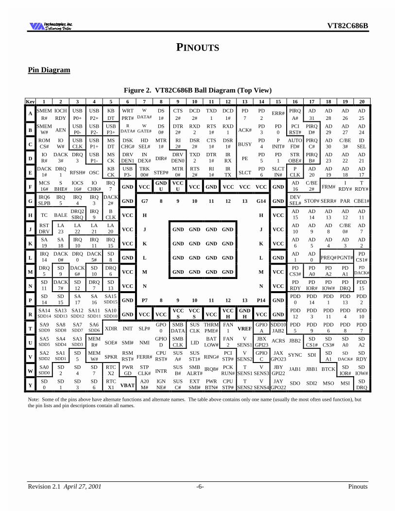
Figure 2. VT82C686B Ball Diagram (Top View)
Key 1 2 3 4 5 6 7 8 9 10 11 12 13 14 15 16 17 18 19 20
A SMEM
R#
IOCH
RDY
USB
P0+
USB
P2+
KB
DT
WRT
PRT#
W
DATA# DS
1#
CTS
2#
DCD
2#
TXD
1
DCD
1#
PD
7
PD
2 ERR# PIRQ
A#
AD
31
AD
28
AD
26
AD
25
B SMEM
W# AEN USB P0-
USB P2-
USB P3+
R DATA#
W GATE#
DS 0#
DTR 2#
RXD 2
RTS 1#
RXD 1 ACK#
PD 3
PD 0
PCI RST#
PIRQ D#
AD 29
AD 27
AD 24
C ROM CS#
IO W#
USB CLK
USB P1+
MS DT
DSK CHG#
HD SEL#
MTR 1#
RI 2#
DSR 2#
CTS 1#
DSR 1# BUSY
PD 4
P INIT#
AUTO FD#
PIRQ C#
AD 30
C/BE 3#
ID SEL
D IO R#
DACK 3#
DRQ 3
USB P1-
MS CK
DRV DEN1
IN DEX# DIR#
DRV DEN0
TXD 2
DTR 1#
IR RX PE
PD 5
PD 1
STR OBE#
PIRQ B#
AD 23
AD 22
AD 21
E DACK
1# DRQ
1 RFSH# OSC KB CK
USB P3-
TRK 00# STEP#
MTR 0#
RTS 2#
RI 1#
IR TX SLCT
PD 6
SLCT IN#
P CLK
AD 20
AD 19
AD 18
AD 17
F MCS 16#
S BHE#
IOCS 16#
IO CHK#
IRQ 7 GND VCC
GND U
VCC U VCC GND VCC VCC VCC GND
AD 16
C/BE 2# FRM#
I RDY#
T RDY#
G IRQ6 SLPB
IRQ 5
IRQ 4
IRQ 3
DACK 2# GND G7 8 9 10 11 12 13 G14 GND
DEV SEL# STOP# SERR# PAR CBE1#
H TC BALE DRQ2 SIRQ
IRQ 9
B CLK VCC H H VCC
AD 15
AD 14
AD 13
AD 12
AD 11
J RST DRV
LA 23
LA 22
LA 21
LA 20 VCC J GND GND GND GND J VCC
AD 10
AD 9
AD 8
C/BE 0#
AD 7
K SA 19
SA 18
IRQ 10
IRQ 11
IRQ 15 VCC K GND GND GND GND K VCC
AD 6
AD 5
AD 4
AD 3
AD 2
L IRQ 14
DACK 0#
DRQ 0
DACK 5#
SD 8 GND L GND GND GND GND L GND
AD 1
AD 0 PREQ# PGNT#
PD CS1#
M DRQ
5 SD 9
DACK 6#
SD 10
DRQ 6 VCC M GND GND GND GND M VCC
PD CS3#
PD A0
PD A2
PD A1
PD DACK#
N SD 11
DACK 7#
SD 12
DRQ 7
SD 13 VCC N N VCC
PD RDY
PD IOR#
PD IOW#
PD DRQ
PDD 15
P SD 14
SD 15
SA 17
SA 16
SA15 SDD15 GND P7 8 9 10 11 12 13 P14 GND
PDD 0
PDD 14
PDD 1
PDD 13
PDD 2
R SA14 SDD14
SA13 SDD13
SA12 SDD12
SA11 SDD11
SA10 SDD10 GND VCC VCC
VCC S
VCC S VCC
VCC H
GND H VCC GND
PDD 12
PDD 3
PDD 11
PDD 4
PDD 10
T SA9 SDD9
SA8 SDD8
SA7 SDD7
SA6 SDD6 XDIR INIT SLP#
GPO 0
SMB DATA
SUS CLK
THRM PME#
FAN 1 VREF
GPIO A
SDD10 JAB2
PDD 5
PDD 9
PDD 6
PDD 8
PDD 7
U SA5 SDD5
SA4 SDD4
SA3 SDD3
MEM R# SOE# SMI# NMI
GPIO D
SMB CLK LID
BAT LOW#
FAN 2
V SENS1
JBX GPI23
ACRS JBB2 SD CS1#
SD CS3#
SD A0
SD A2
V SA2 SDD2
SA1 SDD1
SD 5
MEM W# SPKR
RSM RST# FERR#
CPU RST#
SUS A#
SUS ST1# RING#
PCI STP#
V SENS2
GPIO C
JAX GPO23
SYNC SDI SD A1
SD DACK#
SD RDY
W SA0 SDD0
SD 2
SD 4
SD 7
RTC X2
PWR GD
STP CLK# INTR
SUS B#
SMB ALRT#
IRQ8# PCK RUN#
T SENS1
V SENS3
JBY GPI22
JAB1 JBB1 BTCK SD IOR#
SD IOW#
Y SD 0
SD 1
SD 3
SD 6
RTC X1 VBAT
A20 M#
IGN NE#
SUS C#
EXT SMI#
PWR BTN#
CPU STP#
T SENS2
V SENS4
JAY GPO22
SDO SDI2 MSO MSI SD DRQ
Note: Some of the pins above have alternate functions and alternate names. The table above contains only one name (usually the most often used function), but the pin lists and pin descriptions contain all names.
VT82C686B
Revision 2.1 April 27, 2001 -7- Pinouts
7HFKQRORJLHV ,QF'HOLYHULQJ 9DOXH'HOLYHULQJ 9DOXH
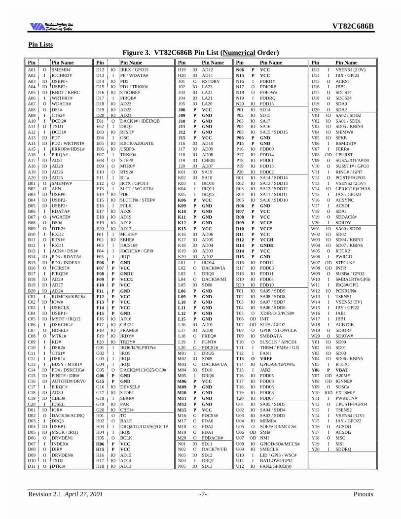
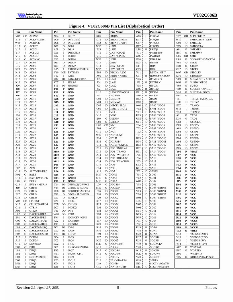
Pin Lists Figure 3. VT82C686B Pin List (Numerical Order)
Pin Pin Name Pin Pin Name Pin Pin Name Pin Pin Name Pin Pin Name A01 O SMEMR# D12 IO IRRX / GPO15 H19 IO AD12 N06 P VCC U13 I VSENS1 (2.0V) A02 I IOCHRDY D13 I PE / WDATA# H20 IO AD11 N15 P VCC U14 I JBX / GPI23 A03 IO USBP0+ D14 IO PD5 J01 O RSTDRV N16 I PDRDY U15 O ACRST A04 IO USBP2+ D15 IO PD1 / TRK00# J02 IO LA23 N17 O PDIOR# U16 I JBB2 A05 IO KBDT / KBRC D16 IO STROBE# J03 IO LA22 N18 O PDIOW# U17 O SDCS1# A06 I WRTPRT# D17 I PIRQB# J04 IO LA21 N19 I PDDRQ U18 O SDCS3# A07 O WDATA# D18 IO AD23 J05 IO LA20 N20 IO PDD15 U19 O SDA0 A08 O DS1# D19 IO AD22 J06 P VCC P01 IO SD14 U20 O SDA2 A09 I CTS2# D20 IO AD21 J09 P GND P02 IO SD15 V01 IO SA02 / SDD2 A10 I DCD2# E01 O DACK1# / IDEIRQB J10 P GND P03 IO SA17 V02 IO SA01 / SDD1 A11 O TXD1 E02 I DRQ1 J11 P GND P04 IO SA16 V03 IO SD05 / KBIN4 A12 I DCD1# E03 IO RFSH# J12 P GND P05 IO SA15 / SDD15 V04 IO MEMW# A13 IO PD7 E04 I OSC J15 P VCC P06 P GND V05 IO SPKR A14 IO PD2 / WRTPRT# E05 IO KBCK/A20GATE J16 IO AD10 P15 P GND V06 I RSMRST# A15 I ERROR#/HDSL# E06 IO USBP3- J17 IO AD09 P16 IO PDD00 V07 I FERR# A16 I PIRQA# E07 I TRK00# J18 IO AD08 P17 IO PDD14 V08 OD CPURST A17 IO AD31 E08 O STEP# J19 IO CBE0# P18 IO PDD01 V09 O SUSA#/O1/APD0 A18 IO AD28 E09 O MTR0# J20 IO AD07 P19 IO PDD13 V10 O SUSST1# / GPO3 A19 IO AD26 E10 O RTS2# K01 IO SA19 P20 IO PDD02 V11 I RING# / GPI7 A20 IO AD25 E11 I RI1# K02 IO SA18 R01 IO SA14 / SDD14 V12 O PCISTP#/GPO5 B01 O SMEMW# E12 O IRTX / GPO14 K03 I IRQ10 R02 IO SA13 / SDD13 V13 I VSENS2 (2.5V) B02 O AEN E13 I SLCT / WGATE# K04 I IRQ11 R03 IO SA12 / SDD12 V14 IO GPIOC(10)/CHAS B03 IO USBP0- E14 IO PD6 K05 I IRQ15 R04 IO SA11 / SDD11 V15 I JAX / GPO23 B04 IO USBP2- E15 IO SLCTIN# / STEP# K06 P VCC R05 IO SA10 / SDD10 V16 O ACSYNC B05 IO USBP3+ E16 I PCLK K09 P GND R06 P GND V17 I ACSDI B06 I RDATA# E17 IO AD20 K10 P GND R07 P VCC V18 O SDA1 B07 O WGATE# E18 IO AD19 K11 P GND R08 P VCC V19 O SDDACK# B08 O DS0# E19 IO AD18 K12 P GND R09 P VCCS V20 I SDRDY B09 O DTR2# E20 IO AD17 K15 P VCC R10 P VCCS W01 IO SA00 / SDD0 B10 I RXD2 F01 I MCS16# K16 IO AD06 R11 P VCC W02 IO SD02 B11 O RTS1# F02 IO SBHE# K17 IO AD05 R12 P VCCH W03 IO SD04 / KBIN3 B12 I RXD1 F03 I IOCS16# K18 IO AD04 R13 P GNDH W04 IO SD07 / KBIN6 B13 I ACK# / DS1# F04 I IOCHCK# / GPI0 K19 IO AD03 R14 P VCC W05 O RTCX2 B14 IO PD3 / RDATA# F05 I IRQ7 K20 IO AD02 R15 P GND W06 I PWRGD B15 IO PD0 / INDEX# F06 P GND L01 I IRQ14 R16 IO PDD12 W07 OD STPCLK# B16 O PCIRST# F07 P VCC L02 O DACK0#/IA R17 IO PDD03 W08 OD INTR B17 I PIRQD# F08 P GNDU L03 I DRQ0 R18 IO PDD11 W09 O SUSB# / GPO2 B18 IO AD29 F09 P VCCU L04 O DACK5#/MI R19 IO PDD04 W10 I SMBALRT#/GPI6 B19 IO AD27 F10 P VCC L05 IO SD08 R20 IO PDD10 W11 I IRQ8#/GPI1 B20 IO AD24 F11 P GND L06 P GND T01 IO SA09 / SDD9 W12 IO PCKRUN# C01 I ROMCS#/KBCS# F12 P VCC L09 P GND T02 IO SA08 / SDD8 W13 I TSENS1 C02 IO IOW# F13 P VCC L10 P GND T03 IO SA07 / SDD7 W14 I VSENS3 (5V) C03 I USBCLK F14 P VCC L11 P GND T04 IO SA06 / SDD6 W15 I JBY / GPI22 C04 IO USBP1+ F15 P GND L12 P GND T05 O XDIR/O12/PCS0# W16 I JAB1 C05 IO MSDT / IRQ12 F16 IO AD16 L15 P GND T06 OD INIT W17 I JBB1 C06 I DSKCHG# F17 IO CBE2# L16 IO AD01 T07 OD SLP# / GPO7 W18 I ACBTCK C07 O HDSEL# F18 IO FRAME# L17 IO AD00 T08 O GPO0 / SLOWCLK W19 O SDIOR# C08 O MTR1# F19 IO IRDY# L18 O PREQ# T09 IO SMBDATA W20 O SDIOW# C09 I RI2# F20 IO TRDY# L19 I PGNT# T10 O SUSCLK / APICD1 Y01 IO SD00 C10 I DSR2# G01 I IRQ6/I4/SLPBTN# L20 O PDCS1# T11 I THRM / PME# / GI5 Y02 IO SD01 C11 I CTS1# G02 I IRQ5 M01 I DRQ5 T12 I FAN1 Y03 IO SD03 C12 I DSR1# G03 I IRQ4 M02 IO SD09 T13 O VREF Y04 IO SD06 / KBIN5 C13 I BUSY / MTR1# G04 I IRQ3 M03 O DACK6#/UA T14 IO GPIOA/8/GPOWE Y05 I RTCX1 C14 IO PD4 / DSKCHG# G05 O DACK2#/I13/O25/OC0# M04 IO SD10 T15 I JAB2 Y06 P VBAT C15 IO PINIT# / DIR# G06 P GND M05 I DRQ6 T16 IO PDD05 Y07 OD A20M# C16 IO AUTOFD#/DRV0 G15 P GND M06 P VCC T17 IO PDD09 Y08 OD IGNNE# C17 I PIRQC# G16 IO DEVSEL# M09 P GND T18 IO PDD06 Y09 O SUSC# C18 IO AD30 G17 IO STOP# M10 P GND T19 IO PDD08 Y10 IOD EXTSMI# C19 IO CBE3# G18 I SERR# M11 P GND T20 IO PDD07 Y11 I PWRBTN# C20 I IDSEL G19 IO PAR M12 P GND U01 IO SA05 / SDD5 Y12 O CPUSTP#/GPO4 D01 IO IOR# G20 IO CBE1# M15 P VCC U02 IO SA04 / SDD4 Y13 I TSENS2 D02 O DACK3#/ACIRQ H01 O TC M16 O PDCS3# U03 IO SA03 / SDD3 Y14 I VSENS4 (12V) D03 I DRQ3 H02 O BALE M17 O PDA0 U04 IO MEMR# Y15 I JAY / GPO22 D04 IO USBP1- H03 I DRQ2/I12/O24/SQ/OC1# M18 O PDA2 U05 O SOE#/O13/MCCS# Y16 O ACSDO D05 IO MSCK / IRQ1 H04 I IRQ9 M19 O PDA1 U06 OD SMI# Y17 I ACSDI2 D06 O DRVDEN1 H05 O BCLK M20 O PDDACK# U07 OD NMI Y18 O MSO D07 I INDEX# H06 P VCC N01 IO SD11 U08 IO GPIOD/SO#/MCCS# Y19 I MSI D08 O DIR# H15 P VCC N02 O DACK7#/UB U09 IO SMBCLK Y20 I SDDRQ D09 O DRVDEN0 H16 IO AD15 N03 IO SD12 U10 I LID / GPI3 / WSC# D10 O TXD2 H17 IO AD14 N04 I DRQ7 U11 I BATLOW#/GPI2 D11 O DTR1# H18 IO AD13 N05 IO SD13 U12 IO FAN2/GPIOB(9)
VT82C686B
Revision 2.1 April 27, 2001 -8- Pinouts
7HFKQRORJLHV ,QF'HOLYHULQJ 9DOXH'HOLYHULQJ 9DOXH
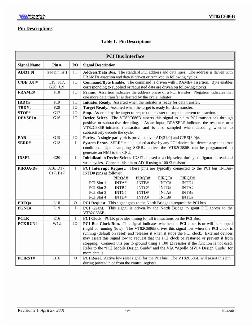
Figure 4. VT82C686B Pin List (Alphabetical Order) Pin Pin Name Pin Pin Name Pin Pin Name Pin Pin Name Pin Pin Name Y07 OD A20M# N04 I DRQ7 K05 I IRQ15 A16 I PIRQA# T07 OD SLP# / GPO7 B13 I ACK# / DS1# D09 O DRVDEN0 D12 IO IRRX / GPO15 D17 I PIRQB# W10 I SMBALRT# / GPI6 W18 I ACBTCK D06 O DRVDEN1 E12 O IRTX / GPO14 C17 I PIRQC# U09 IO SMBCLK U15 O ACRST B08 O DS0# W16 I JAB1 B17 I PIRQD# T09 IO SMBDATA V17 I ACSDI A08 O DS1# T15 I JAB2 L18 O PREQ# A01 O SMEMR# Y17 I ACSDI2 C06 I DSKCHG# V15 I JAX / GPO23 Y11 I PWRBTN# B01 O SMEMW# Y16 O ACSDO C12 I DSR1# Y15 I JAY / GPO22 W06 I PWRGD U06 OD SMI# V16 O ACSYNC C10 I DSR2# W17 I JBB1 B06 I RDATA# U05 O SOE#/GPO13/MCCS# L17 IO AD00 D11 O DTR1# U16 I JBB2 E03 IO RFSH# V05 IO SPKR L16 IO AD01 B09 O DTR2# U14 I JBX / GPI23 E11 I RI1# E08 O STEP# K20 IO AD02 A15 I ERROR#/HDSEL# W15 I JBY / GPI22 C09 I RI2# G17 IO STOP# K19 IO AD03 Y10 IOD EXTSMI# E05 IO KBCK / A20G V11 I RING# / GPI7 W07 OD STPCLK# K18 IO AD04 T12 I FAN1 A05 IO KBDT / KBRC C01 O ROMCS#/KBCS# D16 IO STROBE# K17 IO AD05 U12 IO FAN2/GPIOB(9) J05 IO LA20 V06 I RSMRST# V09 O SUSA# / O1 / APICD0 K16 IO AD06 V07 I FERR# J04 IO LA21 J01 O RSTDRV W09 O SUSB# / GPO2 J20 IO AD07 F18 IO FRAME# J03 IO LA22 Y05 I RTCX1 Y09 O SUSC# J18 IO AD08 F06 P GND J02 IO LA23 W05 O RTCX2 T10 O SUSCLK / APICD1 J17 IO AD09 F11 P GND U10 I LID/GPI3/WSC# B11 O RTS1# V10 O SUSST1# / GPO3 J16 IO AD10 F15 P GND F01 I MCS16# E10 O RTS2# H01 O TC H20 IO AD11 G06 P GND U04 IO MEMR# B12 I RXD1 T11 I THRM / PME# / GI5 H19 IO AD12 G15 P GND V04 IO MEMW# B10 I RXD2 F20 IO TRDY# H18 IO AD13 J09 P GND D05 IO MSCK / IRQ1 W01 IO SA00 / SDD0 E07 I TRK00# H17 IO AD14 J10 P GND C05 IO MSDT / IRQ12 V02 IO SA01 / SDD1 W13 I TSENS1 H16 IO AD15 J11 P GND Y19 I MSI V01 IO SA02 / SDD2 Y13 I TSENS2 F16 IO AD16 J12 P GND Y18 I MSO U03 IO SA03 / SDD3 A11 O TXD1 E20 IO AD17 K09 P GND E09 O MTR0# U02 IO SA04 / SDD4 D10 O TXD2 E19 IO AD18 K10 P GND C08 O MTR1# U01 IO SA05 / SDD5 C03 I USBCLK E18 IO AD19 K11 P GND U07 OD NMI T04 IO SA06 / SDD6 B03 IO USBP0- E17 IO AD20 K12 P GND E04 I OSC T03 IO SA07 / SDD7 A03 IO USBP0+ D20 IO AD21 L06 P GND G19 IO PAR T02 IO SA08 / SDD8 D04 IO USBP1- D19 IO AD22 L09 P GND W12 IO PCKRUN# T01 IO SA09 / SDD9 C04 IO USBP1+ D18 IO AD23 L10 P GND E16 I PCLK R05 IO SA10 / SDD10 B04 IO USBP2- B20 IO AD24 L11 P GND B16 O PCIRST# R04 IO SA11 / SDD11 A04 IO USBP2+ A20 IO AD25 L12 P GND V12 O PCISTP#/GPO5 R03 IO SA12 / SDD12 E06 IO USBP3- A19 IO AD26 L15 P GND B15 IO PD0 / INDEX# R02 IO SA13 / SDD13 B05 IO USBP3+ B19 IO AD27 M09 P GND D15 IO PD1 / TRK00# R01 IO SA14 / SDD14 Y06 P VBAT A18 IO AD28 M10 P GND A14 IO PD2 / WRTPRT# P05 IO SA15 / SDD15 F07 P VCC B18 IO AD29 M11 P GND B14 IO PD3 / RDATA# P04 IO SA16 F10 P VCC C18 IO AD30 M12 P GND C14 IO PD4 / DSKCHG# P03 IO SA17 F12 P VCC A17 IO AD31 P06 P GND D14 IO PD5 K02 IO SA18 F13 P VCC B02 O AEN P15 P GND E14 IO PD6 K01 IO SA19 F14 P VCC C16 IO AUTOFD#/DR0 R06 P GND A13 IO PD7 F02 IO SBHE# H06 P VCC H02 O BALE R15 P GND M17 O PDA0 Y01 IO SD00 H15 P VCC U11 I BATLOW#/GPI2 R13 P GNDH M19 O PDA1 Y02 IO SD01 J06 P VCC H05 O BCLK F08 P GNDU M18 O PDA2 W02 IO SD02 J15 P VCC C13 I BUSY / MTR1# T14 IO GPIOA(8)/GPOWE L20 O PDCS1# Y03 IO SD03 K06 P VCC J19 IO CBE0# V14 IO GPIOC(10)/CHAS M16 O PDCS3# W03 IO SD04 / KBIN3 K15 P VCC G20 IO CBE1# U08 IO GPIOD(11)/MCCS# P16 IO PDD00 V03 IO SD05 / KBIN4 M06 P VCC F17 IO CBE2# T08 O GPO0 / SLOWCLK P18 IO PDD01 Y04 IO SD06 / KBIN5 M15 P VCC C19 IO CBE3# C07 O HDSEL# P20 IO PDD02 W04 IO SD07 / KBIN6 N06 P VCC V08 OD CPURST C20 I IDSEL R17 IO PDD03 L05 IO SD08 N15 P VCC Y12 O CPUSTP#/GPO4 Y08 OD IGNNE# R19 IO PDD04 M02 IO SD09 R07 P VCC C11 I CTS1# D07 I INDEX# T16 IO PDD05 M04 IO SD10 R08 P VCC A09 I CTS2# T06 OD INIT T18 IO PDD06 N01 IO SD11 R11 P VCC L02 O DACK0#/IDEA W08 OD INTR T20 IO PDD07 N03 IO SD12 R14 P VCC E01 O DACK1#/IDEB F04 I IOCHCK# / GPI0 T19 IO PDD08 N05 IO SD13 R12 P VCCH G05 O DAK2#/I13/O25 A02 I IOCHRDY T17 IO PDD09 P01 IO SD14 R09 P VCCS D02 O DACK3#/AIRQ F03 I IOCS16# R20 IO PDD10 P02 IO SD15 R10 P VCCS L04 O DACK5#/MIRQ D01 IO IOR# R18 IO PDD11 U19 O SDA0 F09 P VCCU M03 O DACK6#/USBIA C02 IO IOW# R16 IO PDD12 V18 O SDA1 T13 O VREF N02 O DACK7#/USBIB F19 IO IRDY# P19 IO PDD13 U20 O SDA2 U13 I VSENS1 (2.0V) A12 I DCD1# G04 I IRQ3 P17 IO PDD14 U17 O SDCS1# V13 I VSENS2 (2.2V) A10 I DCD2# G03 I IRQ4 N20 IO PDD15 U18 O SDCS3# W14 I VSENS3 (5V) G16 IO DEVSEL# G02 I IRQ5 M20 O PDDACK# V19 O SDDACK# Y14 I VSENS4 (12V) D08 O DIR# G01 I IRQ6/I4/SLPBTN# N19 I PDDRQ Y20 I SDDRQ A07 O WDATA# L03 I DRQ0 F05 I IRQ7 N17 O PDIOR# W19 O SDIOR# B07 O WGATE# E02 I DRQ1 W11 I IRQ8# / GPI1 N18 O PDIOW# W20 O SDIOW# A06 I WRTPRT# H03 I D2/I12/O24/SQ H04 I IRQ9 N16 I PDRDY V20 I SDRDY T05 O XDIR/GPO12/PCS0# D03 I DRQ3 K03 I IRQ10 D13 I PE / WDATA# G18 I SERR# M01 I DRQ5 K04 I IRQ11 L19 I PGNT# E13 I SLCT / WGATE# M05 I DRQ6 L01 I IRQ14 C15 IO PINIT# / DIR# E15 IO SLCTIN#/STEP#
VT82C686B
Revision 2.1 April 27, 2001 -9- Pinouts
7HFKQRORJLHV ,QF'HOLYHULQJ 9DOXH'HOLYHULQJ 9DOXH
Pin Descriptions
Table 1. Pin Descriptions
PCI Bus Interface
Signal Name Pin # I/O Signal Description
AD[31:0] (see pin list) IO Address/Data Bus. The standard PCI address and data lines. The address is driven with FRAME# assertion and data is driven or received in following cycles.
C/BE[3:0]# C19, F17, G20, J19
IO Command/Byte Enable. The command is driven with FRAME# assertion. Byte enables corresponding to supplied or requested data are driven on following clocks.
FRAME# F18 IO Frame. Assertion indicates the address phase of a PCI transfer. Negation indicates that one more data transfer is desired by the cycle initiator.
IRDY# F19 IO Initiator Ready. Asserted when the initiator is ready for data transfer. TRDY# F20 IO Target Ready. Asserted when the target is ready for data transfer. STOP# G17 IO Stop. Asserted by the target to request the master to stop the current transaction. DEVSEL# G16 IO Device Select. The VT82C686B asserts this signal to claim PCI transactions through
positive or subtractive decoding. As an input, DEVSEL# indicates the response to a VT82C686B-initiated transaction and is also sampled when decoding whether to subtractively decode the cycle.
PAR G19 IO Parity. A single parity bit is provided over AD[31:0] and C/BE[3:0]#. SERR# G18 I System Error. SERR# can be pulsed active by any PCI device that detects a system error
condition. Upon sampling SERR# active, the VT82C686B can be programmed to generate an NMI to the CPU.
IDSEL C20 I Initialization Device Select. IDSEL is used as a chip select during configuration read and write cycles. Connect this pin to AD18 using a 100 Ω resistor.
PIRQA-D# A16, D17, C17, B17
I PCI Interrupt Request. These pins are typically connected to the PCI bus INTA#-INTD# pins as follows: PIRQA# PIRQB# PIRQC# PIRQD# PCI Slot 1 INTA# INTB# INTC# INTD# PCI Slot 2 INTB# INTC# INTD# INTA# PCI Slot 3 INTC# INTD# INTA# INTB# PCI Slot 4 INTD# INTA# INTB# INTC#
PREQ# L18 O PCI Request. This signal goes to the North Bridge to request the PCI bus. PGNT# L19 I PCI Grant. This signal is driven by the North Bridge to grant PCI access to the
VT82C686B. PCLK E16 I PCI Clock. PCLK provides timing for all transactions on the PCI Bus. PCKRUN# W12 IO PCI Bus Clock Run. This signal indicates whether the PCI clock is or will be stopped
(high) or running (low). The VT82C686B drives this signal low when the PCI clock is running (default on reset) and releases it when it stops the PCI clock. External devices may assert this signal low to request that the PCI clock be restarted or prevent it from stopping. Connect this pin to ground using a 100 Ω resistor if the function is not used. Refer to the “PCI Mobile Design Guide” and the VIA “Apollo MVP4 Design Guide” for more details.
PCIRST# B16 O PCI Reset. Active low reset signal for the PCI bus. The VT82C686B will assert this pin during power-up or from the control register.
VT82C686B
Revision 2.1 April 27, 2001 -10- Pinouts
7HFKQRORJLHV ,QF'HOLYHULQJ 9DOXH'HOLYHULQJ 9DOXH
CPU Interface
Signal Name Pin # I/O Signal Description
CPURST V8 OD CPU Reset. The VT82C686B asserts CPURST to reset the CPU during power-up.
INTR W8 OD CPU Interrupt. INTR is driven by the VT82C686B to signal the CPU that an interrupt request is pending and needs service.
NMI U7 OD Non-Maskable Interrupt. NMI is used to force a non-maskable interrupt to the CPU. The VT82C686B generates an NMI when either SERR# or IOCHK# is asserted.
INIT T6 OD Initialization. The VT82C686B asserts INIT if it detects a shut-down special cycle on the PCI bus or if a soft reset is initiated by the register
STPCLK# W7 OD Stop Clock. STPCLK# is asserted by the VT82C686B to the CPU to throttle the processor clock.
SMI# U6 OD System Management Interrupt. SMI# is asserted by the VT82C686B to the CPU in response to different Power-Management events.
FERR# V7 I Numerical Coprocessor Error. This signal is tied to the coprocessor error signal on the CPU. Internally generates interrupt 13 if active. 1.5V interface.
IGNNE# Y8 OD Ignore Numeric Error. This pin is connected to the “ignore error” pin on the CPU.
SLP# / GPO7 T7 OD Sleep (Rx75[7] = 0). Used to put the CPU to sleep. Used with slot-1 CPUs only. Not currently used with socket-7 CPUs.
A20M# Y7 OD A20 Mask. Connect to A20 mask input of the CPU to control address bit-20 generation. Logical combination of the A20GATE input (from internal or external keyboard controller) and Port 92 bit-1 (Fast_A20).
Note: Connect each of the above signals to 4.7K Ω pullup resistors to VCC3.
Advanced Programmable Interrupt Controller (APIC)
Signal Name Pin # I/O Signal Description
WSC# / GPI3 / LID U10 I Write Snoop Complete. Asserted by the north bridge to indicate that all snoop activity on the CPU bus initiated by the last PCI-to-DRAM write is complete and that it is safe to perform an APIC interrupt.
APICD0 / GPO1 / SUSA# V9 IO APIC Data 0. 1.5V interface. APICD1 / SUSCLK T10 IO APIC Data 1. 1.5V interface. For programming information, refer to Function 0 Rx74,77, Function 4 Rx54[3-2], and Memory Mapped / Indexed APIC registers. Rx77[4] is “Internal APIC Enable”. The clock source used by the chip to clock the internal I/O APIC is OSC (14.31818 MHz), so OSC must be externally connected to the CPU I/O APIC clock input.
VT82C686B
Revision 2.1 April 27, 2001 -11- Pinouts
7HFKQRORJLHV ,QF'HOLYHULQJ 9DOXH'HOLYHULQJ 9DOXH
Universal Serial Bus Interface
Signal Name Pin # I/O Signal Description
USBP0+ A3 IO USB Port 0 Data + USBP0- B3 IO USB Port 0 Data - USBP1+ C4 IO USB Port 1 Data + USBP1- D4 IO USB Port 1 Data - USBP2+ A4 IO USB Port 2 Data + USBP2- B4 IO USB Port 2 Data - USBP3+ B5 IO USB Port 3 Data + USBP3- E6 IO USB Port 3 Data - USBCLK C3 I USB Clock. 48MHz clock input for the USB interface USBOC0# / GPO25 / DACK2# / FDCIRQ G5 I USB Port 0 Over Current Detect. Port 0 is disabled if low.
USBOC0# if Rx76[7] = 1 and Rx76[6] = 0 USBOC1# / GPO24 / DRQ2 / FDCDRQ / SERIRQ
H3 I USB Port 1 Over Current Detect. Port 1 is disabled if this input is low. Direct inputs are provided for overcurrent protection for ports 0 and 1 which may be used if the alternate functions of these two pins are not required. If overcurrent protection is desired on all four ports (or it is desired to use the alternate functions of these two pins), an external buffer may be used to drive the state of USBOC[3-0]# onto SD[3-0] during ISA bus refresh cycles (i.e., while ISA bus RFSH# is low, so that RFSH# may be used as the buffer enable). USCOC1# if Rx76[7] = 1 and Rx76[6] = 0.
USBOC0# (SD2 & RFSH#) (W2) I USB Port 0 Over Current Detect USBOC1# (SD1 & RFSH#) (Y2) I USB Port 1 Over Current Detect USBOC2# (SD0 & RFSH#) (Y1) I USB Port 2 Over Current Detect USBOC3# (SD3 & RFSH#) (Y3) I USB Port 3 Over Current Detect USBIRQA / DACK6# M3 O USB Interrupt Request A. Output of internal block. USBIRQB / DACK7# N2 O USB Interrupt Request B. Output of internal block.
System Management Bus (SMB) Interface (I2C Bus)
Signal Name Pin # I/O Signal Description
SMBCLK U9 IO SMB / I2C Clock. SMBDATA T9 IO SMB / I2C Data. SMBALRT# / GPI6 W10 I SMB Alert. (System Management Bus I/O space Rx08[3] = 1)
When the chip is enabled to allow it, assertion generates an IRQ or SMI interrupt or a power management resume event. The same pin is used as General Purpose Input 6 whose value is reflected in Rx48[6] of function 4 I/O space
VT82C686B
Revision 2.1 April 27, 2001 -12- Pinouts
7HFKQRORJLHV ,QF'HOLYHULQJ 9DOXH'HOLYHULQJ 9DOXH
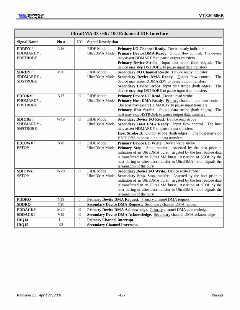
UltraDMA-33 / 66 / 100 Enhanced IDE Interface
Signal Name Pin # I/O Signal Description
PDRDY / PDDMARDY / PDSTROBE
N16 I EIDE Mode: Primary I/O Channel Ready. Device ready indicator UltraDMA Mode: Primary Device DMA Ready. Output flow control. The device
may assert DDMARDY to pause output transfers Primary Device Strobe. Input data strobe (both edges). The
device may stop DSTROBE to pause input data transfers SDRDY / SDDMARDY / SDSTROBE
V20 I EIDE Mode: Secondary I/O Channel Ready. Device ready indicator UltraDMA Mode: Secondary Device DMA Ready. Output flow control. The
device may assert DDMARDY to pause output transfers Secondary Device Strobe. Input data strobe (both edges). The
device may stop DSTROBE to pause input data transfers PDIOR# / PHDMARDY / PHSTROBE
N17 O EIDE Mode: Primary Device I/O Read. Device read strobe UltraDMA Mode: Primary Host DMA Ready. Primary channel input flow control.
The host may assert HDMARDY to pause input transfers Primary Host Strobe. Output data strobe (both edges). The
host may stop HSTROBE to pause output data transfers SDIOR# / SHDMARDY / SHSTROBE
W19 O EIDE Mode: Secondary Device I/O Read. Device read strobe UltraDMA Mode: Secondary Host DMA Ready. Input flow control. The host
may assert HDMARDY to pause input transfers Host Strobe B. Output strobe (both edges). The host may stop
HSTROBE to pause output data transfers PDIOW# / PSTOP
N18 O EIDE Mode: Primary Device I/O Write. Device write strobe UltraDMA Mode: Primary Stop. Stop transfer: Asserted by the host prior to
initiation of an UltraDMA burst; negated by the host before data is transferred in an UltraDMA burst. Assertion of STOP by the host during or after data transfer in UltraDMA mode signals the termination of the burst.
SDIOW# / SSTOP
W20 O EIDE Mode: Secondary Device I/O Write. Device write strobe UltraDMA Mode: Secondary Stop. Stop transfer: Asserted by the host prior to
initiation of an UltraDMA burst; negated by the host before data is transferred in an UltraDMA burst. Assertion of STOP by the host during or after data transfer in UltraDMA mode signals the termination of the burst.
PDDRQ N19 I Primary Device DMA Request. Primary channel DMA request SDDRQ Y20 I Secondary Device DMA Request. Secondary channel DMA request PDDACK# M20 O Primary Device DMA Acknowledge. Primary channel DMA acknowledge SDDACK# V19 O Secondary Device DMA Acknowledge. Secondary channel DMA acknowledge IRQ14 L1 I Primary Channel Interrupt. IRQ15 K5 I Secondary Channel Interrupt.
VT82C686B
Revision 2.1 April 27, 2001 -13- Pinouts
7HFKQRORJLHV ,QF'HOLYHULQJ 9DOXH'HOLYHULQJ 9DOXH
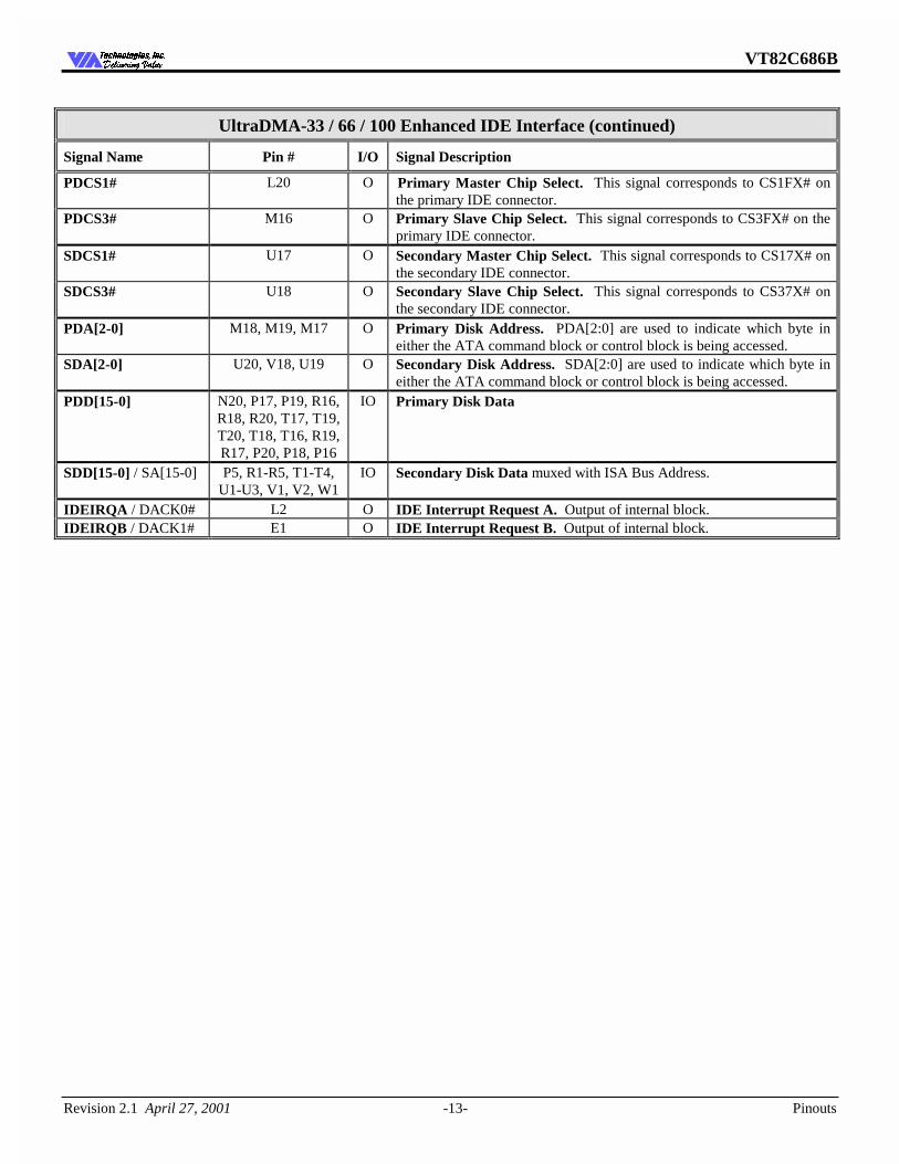
UltraDMA-33 / 66 / 100 Enhanced IDE Interface (continued)
Signal Name Pin # I/O Signal Description
PDCS1# L20 O Primary Master Chip Select. This signal corresponds to CS1FX# on the primary IDE connector.
PDCS3# M16 O Primary Slave Chip Select. This signal corresponds to CS3FX# on the primary IDE connector.
SDCS1# U17 O Secondary Master Chip Select. This signal corresponds to CS17X# on the secondary IDE connector.
SDCS3# U18 O Secondary Slave Chip Select. This signal corresponds to CS37X# on the secondary IDE connector.
PDA[2-0] M18, M19, M17 O Primary Disk Address. PDA[2:0] are used to indicate which byte in either the ATA command block or control block is being accessed.
SDA[2-0] U20, V18, U19 O Secondary Disk Address. SDA[2:0] are used to indicate which byte in either the ATA command block or control block is being accessed.
PDD[15-0] N20, P17, P19, R16, R18, R20, T17, T19, T20, T18, T16, R19, R17, P20, P18, P16
IO Primary Disk Data
SDD[15-0] / SA[15-0] P5, R1-R5, T1-T4, U1-U3, V1, V2, W1
IO Secondary Disk Data muxed with ISA Bus Address.
IDEIRQA / DACK0# L2 O IDE Interrupt Request A. Output of internal block. IDEIRQB / DACK1# E1 O IDE Interrupt Request B. Output of internal block.
VT82C686B
Revision 2.1 April 27, 2001 -14- Pinouts
7HFKQRORJLHV ,QF'HOLYHULQJ 9DOXH'HOLYHULQJ 9DOXH
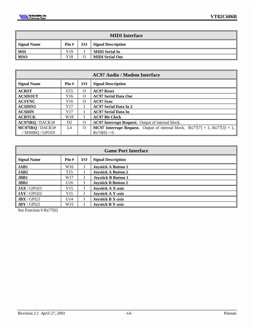
MIDI Interface
Signal Name Pin # I/O Signal Description
MSI Y19 I MIDI Serial In MSO Y18 O MIDI Serial Out
AC97 Audio / Modem Interface
Signal Name Pin # I/O Signal Description
ACRST U15 O AC97 Reset ACSDOUT Y16 O AC97 Serial Data Out ACSYNC V16 O AC97 Sync ACSDIN2 Y17 I AC97 Serial Data In 2 ACSDIN V17 I AC97 Serial Data In ACBTCK W18 I AC97 Bit Clock AC97IRQ / DACK3# D2 O AC97 Interrupt Request. Output of internal block. MC97IRQ / DACK5# / SERIRQ / GPO19
L4 O MC97 Interrupt Request. Output of internal block. Rx77[7] = 1, Rx77[3] = 1, Rx74[6] = 0.
Game Port Interface
Signal Name Pin # I/O Signal Description
JAB1 W16 I Joystick A Button 1 JAB2 T15 I Joystick A Button 2 JBB1 W17 I Joystick B Button 1 JBB2 U16 I Joystick B Button 2 JAX / GPO23 V15 I Joystick A X-axis JAY / GPO22 Y15 I Joystick A Y-axis JBX / GPI23 U14 I Joystick B X-axis JBY / GPI22 W15 I Joystick B Y-axis See Function 0 Rx77[6]
VT82C686B
Revision 2.1 April 27, 2001 -15- Pinouts
7HFKQRORJLHV ,QF'HOLYHULQJ 9DOXH'HOLYHULQJ 9DOXH
Floppy Disk Interface
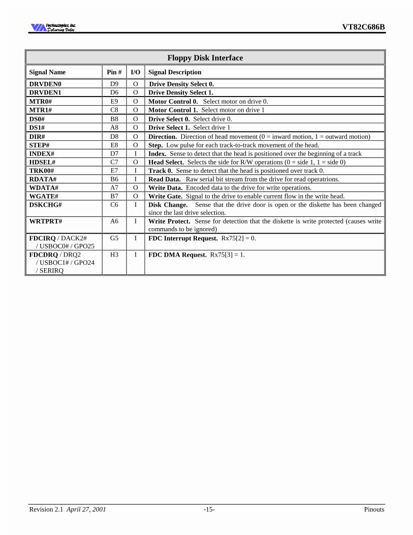
Signal Name Pin # I/O Signal Description
DRVDEN0 D9 O Drive Density Select 0. DRVDEN1 D6 O Drive Density Select 1. MTR0# E9 O Motor Control 0. Select motor on drive 0. MTR1# C8 O Motor Control 1. Select motor on drive 1 DS0# B8 O Drive Select 0. Select drive 0. DS1# A8 O Drive Select 1. Select drive 1 DIR# D8 O Direction. Direction of head movement (0 = inward motion, 1 = outward motion) STEP# E8 O Step. Low pulse for each track-to-track movement of the head. INDEX# D7 I Index. Sense to detect that the head is positioned over the beginning of a track HDSEL# C7 O Head Select. Selects the side for R/W operations (0 = side 1, 1 = side 0) TRK00# E7 I Track 0. Sense to detect that the head is positioned over track 0. RDATA# B6 I Read Data. Raw serial bit stream from the drive for read operatrions. WDATA# A7 O Write Data. Encoded data to the drive for write operations. WGATE# B7 O Write Gate. Signal to the drive to enable current flow in the write head. DSKCHG# C6 I Disk Change. Sense that the drive door is open or the diskette has been changed
since the last drive selection. WRTPRT# A6 I Write Protect. Sense for detection that the diskette is write protected (causes write
commands to be ignored) FDCIRQ / DACK2# / USBOC0# / GPO25
G5 I FDC Interrupt Request. Rx75[2] = 0.
FDCDRQ / DRQ2 / USBOC1# / GPO24 / SERIRQ
H3 I FDC DMA Request. Rx75[3] = 1.
VT82C686B
Revision 2.1 April 27, 2001 -16- Pinouts
7HFKQRORJLHV ,QF'HOLYHULQJ 9DOXH'HOLYHULQJ 9DOXH
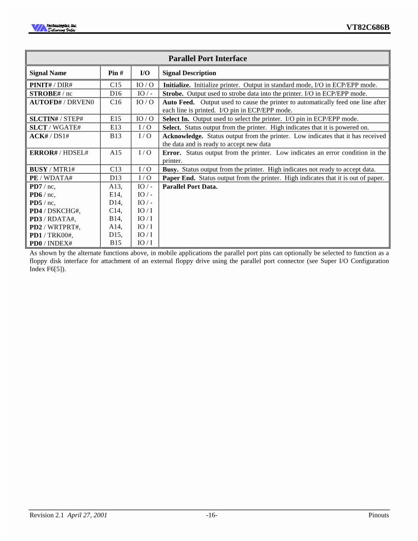
Parallel Port Interface
Signal Name Pin # I/O Signal Description
PINIT# / DIR# C15 IO / O Initialize. Initialize printer. Output in standard mode, I/O in ECP/EPP mode. STROBE# / nc D16 IO / - Strobe. Output used to strobe data into the printer. I/O in ECP/EPP mode. AUTOFD# / DRVEN0 C16 IO / O Auto Feed. Output used to cause the printer to automatically feed one line after
each line is printed. I/O pin in ECP/EPP mode. SLCTIN# / STEP# E15 IO / O Select In. Output used to select the printer. I/O pin in ECP/EPP mode. SLCT / WGATE# E13 I / O Select. Status output from the printer. High indicates that it is powered on. ACK# / DS1# B13 I / O Acknowledge. Status output from the printer. Low indicates that it has received
the data and is ready to accept new data ERROR# / HDSEL# A15 I / O Error. Status output from the printer. Low indicates an error condition in the
printer. BUSY / MTR1# C13 I / O Busy. Status output from the printer. High indicates not ready to accept data. PE / WDATA# D13 I / O Paper End. Status output from the printer. High indicates that it is out of paper. PD7 / nc, PD6 / nc, PD5 / nc, PD4 / DSKCHG#, PD3 / RDATA#, PD2 / WRTPRT#, PD1 / TRK00#, PD0 / INDEX#
A13, E14, D14, C14, B14, A14, D15, B15
IO / - IO / - IO / - IO / I IO / I IO / I IO / I IO / I
Parallel Port Data.
As shown by the alternate functions above, in mobile applications the parallel port pins can optionally be selected to function as a floppy disk interface for attachment of an external floppy drive using the parallel port connector (see Super I/O Configuration Index F6[5]).
VT82C686B
Revision 2.1 April 27, 2001 -17- Pinouts
7HFKQRORJLHV ,QF'HOLYHULQJ 9DOXH'HOLYHULQJ 9DOXH
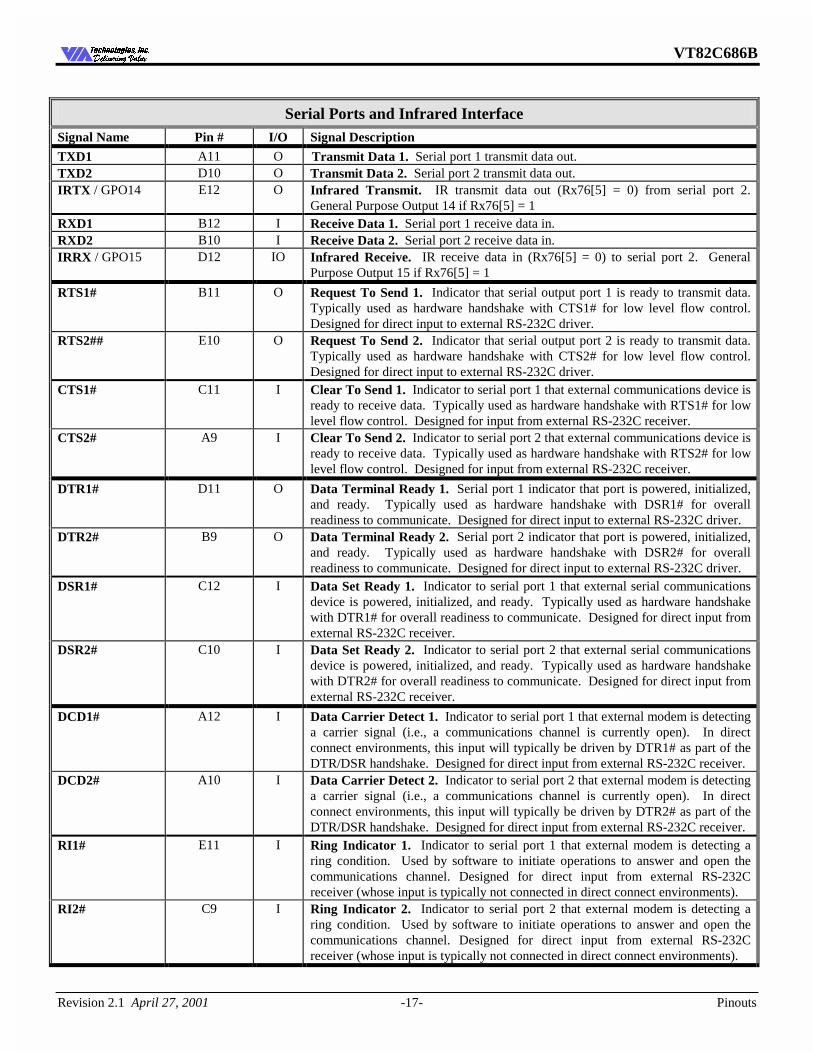
Serial Ports and Infrared Interface Signal Name Pin # I/O Signal Description
TXD1 A11 O Transmit Data 1. Serial port 1 transmit data out. TXD2 D10 O Transmit Data 2. Serial port 2 transmit data out. IRTX / GPO14 E12 O Infrared Transmit. IR transmit data out (Rx76[5] = 0) from serial port 2.
General Purpose Output 14 if Rx76[5] = 1 RXD1 B12 I Receive Data 1. Serial port 1 receive data in. RXD2 B10 I Receive Data 2. Serial port 2 receive data in. IRRX / GPO15 D12 IO Infrared Receive. IR receive data in (Rx76[5] = 0) to serial port 2. General
Purpose Output 15 if Rx76[5] = 1
RTS1# B11 O Request To Send 1. Indicator that serial output port 1 is ready to transmit data. Typically used as hardware handshake with CTS1# for low level flow control. Designed for direct input to external RS-232C driver.
RTS2## E10 O Request To Send 2. Indicator that serial output port 2 is ready to transmit data. Typically used as hardware handshake with CTS2# for low level flow control. Designed for direct input to external RS-232C driver.
CTS1# C11 I Clear To Send 1. Indicator to serial port 1 that external communications device is ready to receive data. Typically used as hardware handshake with RTS1# for low level flow control. Designed for input from external RS-232C receiver.
CTS2# A9 I Clear To Send 2. Indicator to serial port 2 that external communications device is ready to receive data. Typically used as hardware handshake with RTS2# for low level flow control. Designed for input from external RS-232C receiver.
DTR1# D11 O Data Terminal Ready 1. Serial port 1 indicator that port is powered, initialized, and ready. Typically used as hardware handshake with DSR1# for overall readiness to communicate. Designed for direct input to external RS-232C driver.
DTR2# B9 O Data Terminal Ready 2. Serial port 2 indicator that port is powered, initialized, and ready. Typically used as hardware handshake with DSR2# for overall readiness to communicate. Designed for direct input to external RS-232C driver.
DSR1# C12 I Data Set Ready 1. Indicator to serial port 1 that external serial communications device is powered, initialized, and ready. Typically used as hardware handshake with DTR1# for overall readiness to communicate. Designed for direct input from external RS-232C receiver.
DSR2# C10 I Data Set Ready 2. Indicator to serial port 2 that external serial communications device is powered, initialized, and ready. Typically used as hardware handshake with DTR2# for overall readiness to communicate. Designed for direct input from external RS-232C receiver.
DCD1# A12 I Data Carrier Detect 1. Indicator to serial port 1 that external modem is detecting a carrier signal (i.e., a communications channel is currently open). In direct connect environments, this input will typically be driven by DTR1# as part of the DTR/DSR handshake. Designed for direct input from external RS-232C receiver.
DCD2# A10 I Data Carrier Detect 2. Indicator to serial port 2 that external modem is detecting a carrier signal (i.e., a communications channel is currently open). In direct connect environments, this input will typically be driven by DTR2# as part of the DTR/DSR handshake. Designed for direct input from external RS-232C receiver.
RI1# E11 I Ring Indicator 1. Indicator to serial port 1 that external modem is detecting a ring condition. Used by software to initiate operations to answer and open the communications channel. Designed for direct input from external RS-232C receiver (whose input is typically not connected in direct connect environments).
RI2# C9 I Ring Indicator 2. Indicator to serial port 2 that external modem is detecting a ring condition. Used by software to initiate operations to answer and open the communications channel. Designed for direct input from external RS-232C receiver (whose input is typically not connected in direct connect environments).
VT82C686B
Revision 2.1 April 27, 2001 -18- Pinouts
7HFKQRORJLHV ,QF'HOLYHULQJ 9DOXH'HOLYHULQJ 9DOXH
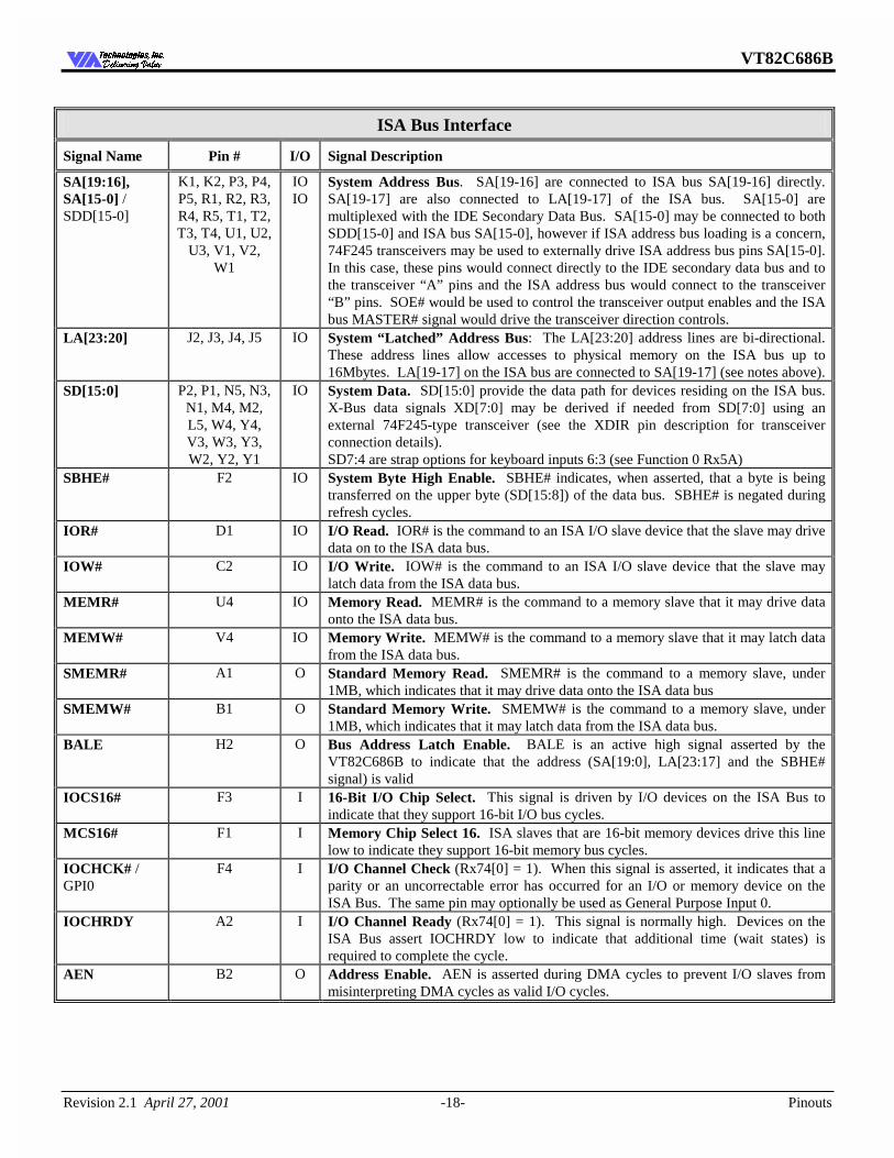
ISA Bus Interface
Signal Name Pin # I/O Signal Description
SA[19:16], SA[15-0] / SDD[15-0]
K1, K2, P3, P4, P5, R1, R2, R3, R4, R5, T1, T2, T3, T4, U1, U2,
U3, V1, V2, W1
IO IO
System Address Bus. SA[19-16] are connected to ISA bus SA[19-16] directly. SA[19-17] are also connected to LA[19-17] of the ISA bus. SA[15-0] are multiplexed with the IDE Secondary Data Bus. SA[15-0] may be connected to both SDD[15-0] and ISA bus SA[15-0], however if ISA address bus loading is a concern, 74F245 transceivers may be used to externally drive ISA address bus pins SA[15-0]. In this case, these pins would connect directly to the IDE secondary data bus and to the transceiver “A” pins and the ISA address bus would connect to the transceiver “B” pins. SOE# would be used to control the transceiver output enables and the ISA bus MASTER# signal would drive the transceiver direction controls.
LA[23:20] J2, J3, J4, J5 IO System “Latched” Address Bus: The LA[23:20] address lines are bi-directional. These address lines allow accesses to physical memory on the ISA bus up to 16Mbytes. LA[19-17] on the ISA bus are connected to SA[19-17] (see notes above).
SD[15:0] P2, P1, N5, N3, N1, M4, M2, L5, W4, Y4, V3, W3, Y3, W2, Y2, Y1
IO System Data. SD[15:0] provide the data path for devices residing on the ISA bus. X-Bus data signals XD[7:0] may be derived if needed from SD[7:0] using an external 74F245-type transceiver (see the XDIR pin description for transceiver connection details). SD7:4 are strap options for keyboard inputs 6:3 (see Function 0 Rx5A)
SBHE# F2 IO System Byte High Enable. SBHE# indicates, when asserted, that a byte is being transferred on the upper byte (SD[15:8]) of the data bus. SBHE# is negated during refresh cycles.
IOR# D1 IO I/O Read. IOR# is the command to an ISA I/O slave device that the slave may drive data on to the ISA data bus.
IOW# C2 IO I/O Write. IOW# is the command to an ISA I/O slave device that the slave may latch data from the ISA data bus.
MEMR# U4 IO Memory Read. MEMR# is the command to a memory slave that it may drive data onto the ISA data bus.
MEMW# V4 IO Memory Write. MEMW# is the command to a memory slave that it may latch data from the ISA data bus.
SMEMR# A1 O Standard Memory Read. SMEMR# is the command to a memory slave, under 1MB, which indicates that it may drive data onto the ISA data bus
SMEMW# B1 O Standard Memory Write. SMEMW# is the command to a memory slave, under 1MB, which indicates that it may latch data from the ISA data bus.
BALE H2 O Bus Address Latch Enable. BALE is an active high signal asserted by the VT82C686B to indicate that the address (SA[19:0], LA[23:17] and the SBHE# signal) is valid
IOCS16# F3 I 16-Bit I/O Chip Select. This signal is driven by I/O devices on the ISA Bus to indicate that they support 16-bit I/O bus cycles.
MCS16# F1 I Memory Chip Select 16. ISA slaves that are 16-bit memory devices drive this line low to indicate they support 16-bit memory bus cycles.
IOCHCK# / GPI0
F4 I I/O Channel Check (Rx74[0] = 1). When this signal is asserted, it indicates that a parity or an uncorrectable error has occurred for an I/O or memory device on the ISA Bus. The same pin may optionally be used as General Purpose Input 0.
IOCHRDY A2 I I/O Channel Ready (Rx74[0] = 1). This signal is normally high. Devices on the ISA Bus assert IOCHRDY low to indicate that additional time (wait states) is required to complete the cycle.
AEN B2 O Address Enable. AEN is asserted during DMA cycles to prevent I/O slaves from misinterpreting DMA cycles as valid I/O cycles.
VT82C686B
Revision 2.1 April 27, 2001 -19- Pinouts
7HFKQRORJLHV ,QF'HOLYHULQJ 9DOXH'HOLYHULQJ 9DOXH
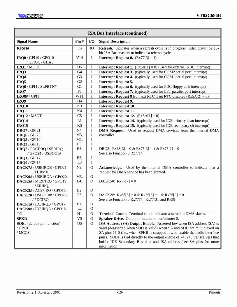
ISA Bus Interface (continued)
Signal Name Pin # I/O Signal Description
RFSH# E3 IO Refresh. Indicates when a refresh cycle is in progress. Also driven by 16-bit ISA Bus masters to indicate a refresh cycle.
IRQ0 / GPI10 / GPO10 / GPIOC / CHAS
V14 I Interrupt Request 0. (Rx77[3] = 1)
IRQ1 / MSCK D5 I Interrupt Request 1. (Rx5A[1] = 0) (used for external KBC interrupt) IRQ3 G4 I Interrupt Request 3. (typically used for COM2 serial port interrupt) IRQ4 G3 I Interrupt Request 4. (typically used for COM1 serial port interrupt) IRQ5 G2 I Interrupt Request 5. IRQ6 / GPI4 / SLPBTN# G1 I Interrupt Request 6. (typically used for FDC floppy ctrlr interrupt) IRQ7 F5 I Interrupt Request 7. (typically used for LPT parallel port interrupt) IRQ8# / GPI1 W11 I Interrupt Request 8 from ext RTC if int RTC disabled (Rx5A[2] = 0) IRQ9 H4 I Interrupt Request 9. IRQ10 K3 I Interrupt Request 10. IRQ11 K4 I Interrupt Request 11. IRQ12 / MSDT C5 I Interrupt Request 12. (Rx5A[1] = 0) IRQ14 L1 I Interrupt Request 14. (typically used for IDE primary chan interrupt) IRQ15 K5 I Interrupt Request 15. (typically used for IDE secondary ch interrupt) DRQ7 / GPI21, DRQ6 / GPI20, DRQ5 / GPI19, DRQ3 / GPI18, DRQ2 / FDCDRQ / SERIRQ / GPO24 / USBOC1# DRQ1 / GPI17, DRQ0 / GPI16
N4, M5, M1, D3, H3,
E2, L3
I I I I I I I
DMA Request. Used to request DMA services from the internal DMA controller. DRQ2: Rx68[3] = 0 & Rx75[3] = 1 & Rx75[1] = 0 See also Function 0 Rx77[7]
DACK7# / USBIRQB / GPO21 / THRM#, DACK6# / USBIRQA / GPO20, DACK5# / MC97IRQ / GPO19 / SERIRQ, DACK3# / AC97IRQ / GPO18, DACK2# / USBOC0# / GPO25 / FDCIRQ DACK1# / IDEIRQB / GPO17, DACK0# / IDEIRQA / GPO16
N2,
M3, L4,
D2, G5,
E1, L2
O
O O
O O
O O
Acknowledge. Used by the internal DMA controller to indicate that a request for DMA service has been granted. DACK5#: Rx77[7] = 0 DACK2#: Rx68[3] = 0 & Rx75[3] = 1 & Rx75[2] = 0 See also Function 0 Rx77[7], Rx77[3], and Rx58
TC H1 O Terminal Count. Terminal count indicator asserted to DMA slaves. SPKR V5 O Speaker Drive. Output of internal timer/counter 2. SOE# (default pin function) / GPO13 / MCCS#
U5 O ISA Address (SA) Output Enable. Asserted low when ISA address (SA) is valid (deasserted when SDD is valid) when SA and SDD are multiplexed on SA pins 15-0 (i.e., when SPKR is strapped low to enable the audio interface pins). SOE# is tied directly to the output enable of 74F245 transceivers that buffer IDE Secondary Bus data and ISA-address (see SA pins for more information).
VT82C686B
Revision 2.1 April 27, 2001 -20- Pinouts
7HFKQRORJLHV ,QF'HOLYHULQJ 9DOXH'HOLYHULQJ 9DOXH
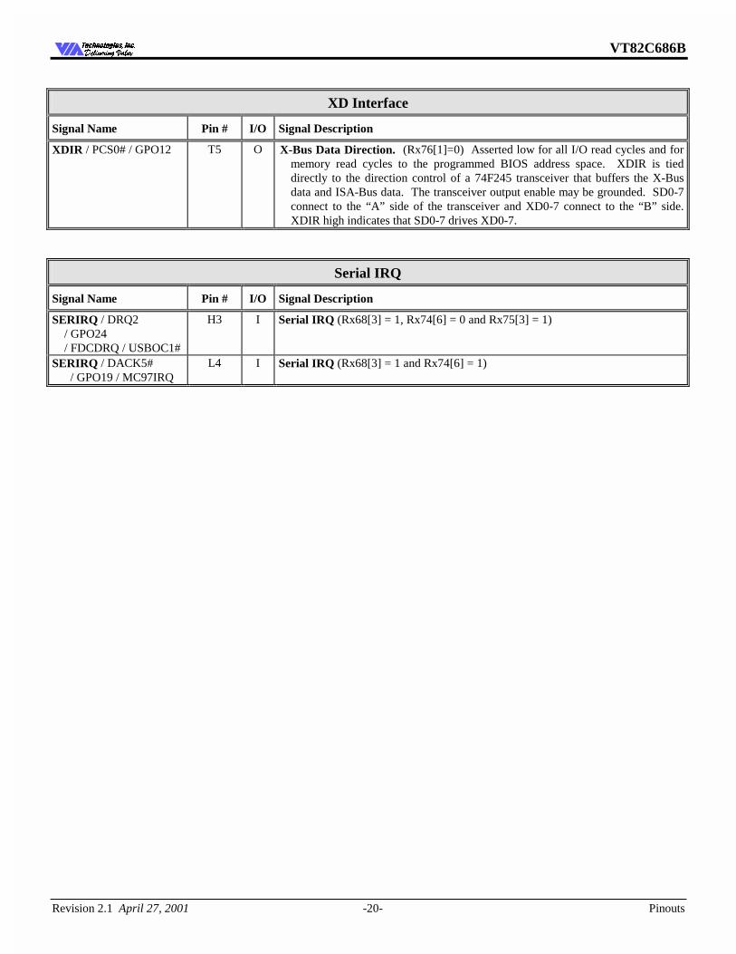
XD Interface
Signal Name Pin # I/O Signal Description
XDIR / PCS0# / GPO12 T5 O X-Bus Data Direction. (Rx76[1]=0) Asserted low for all I/O read cycles and for memory read cycles to the programmed BIOS address space. XDIR is tied directly to the direction control of a 74F245 transceiver that buffers the X-Bus data and ISA-Bus data. The transceiver output enable may be grounded. SD0-7 connect to the “A” side of the transceiver and XD0-7 connect to the “B” side. XDIR high indicates that SD0-7 drives XD0-7.
Serial IRQ
Signal Name Pin # I/O Signal Description
SERIRQ / DRQ2 / GPO24 / FDCDRQ / USBOC1#
H3 I Serial IRQ (Rx68[3] = 1, Rx74[6] = 0 and Rx75[3] = 1)
SERIRQ / DACK5# / GPO19 / MC97IRQ
L4 I Serial IRQ (Rx68[3] = 1 and Rx74[6] = 1)
VT82C686B
Revision 2.1 April 27, 2001 -21- Pinouts
7HFKQRORJLHV ,QF'HOLYHULQJ 9DOXH'HOLYHULQJ 9DOXH
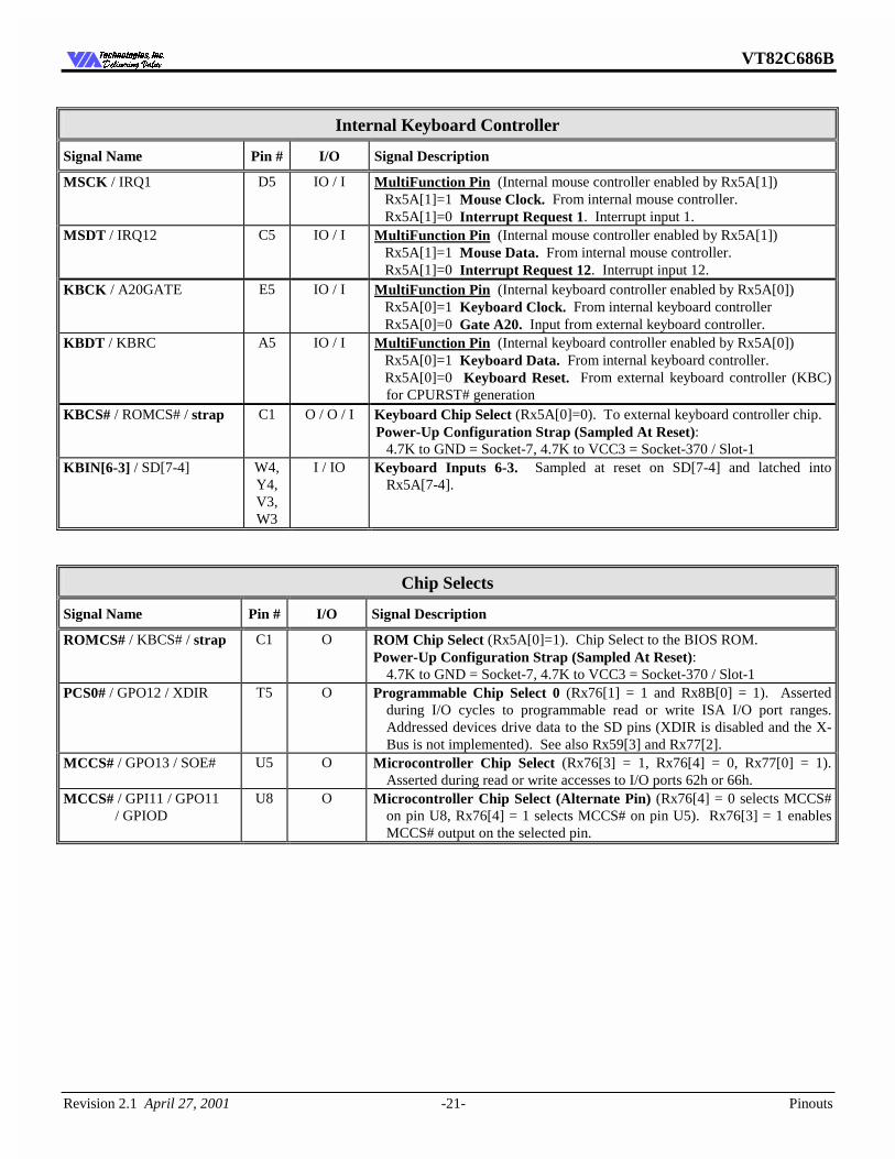
Internal Keyboard Controller
Signal Name Pin # I/O Signal Description
MSCK / IRQ1 D5 IO / I MultiFunction Pin (Internal mouse controller enabled by Rx5A[1]) Rx5A[1]=1 Mouse Clock. From internal mouse controller. Rx5A[1]=0 Interrupt Request 1. Interrupt input 1.
MSDT / IRQ12 C5 IO / I MultiFunction Pin (Internal mouse controller enabled by Rx5A[1]) Rx5A[1]=1 Mouse Data. From internal mouse controller. Rx5A[1]=0 Interrupt Request 12. Interrupt input 12.
KBCK / A20GATE E5 IO / I MultiFunction Pin (Internal keyboard controller enabled by Rx5A[0]) Rx5A[0]=1 Keyboard Clock. From internal keyboard controller Rx5A[0]=0 Gate A20. Input from external keyboard controller.
KBDT / KBRC A5 IO / I MultiFunction Pin (Internal keyboard controller enabled by Rx5A[0]) Rx5A[0]=1 Keyboard Data. From internal keyboard controller. Rx5A[0]=0 Keyboard Reset. From external keyboard controller (KBC)
for CPURST# generation KBCS# / ROMCS# / strap C1 O / O / I Keyboard Chip Select (Rx5A[0]=0). To external keyboard controller chip.
Power-Up Configuration Strap (Sampled At Reset): 4.7K to GND = Socket-7, 4.7K to VCC3 = Socket-370 / Slot-1
KBIN[6-3] / SD[7-4] W4, Y4, V3, W3
I / IO Keyboard Inputs 6-3. Sampled at reset on SD[7-4] and latched into Rx5A[7-4].
Chip Selects
Signal Name Pin # I/O Signal Description
ROMCS# / KBCS# / strap C1 O ROM Chip Select (Rx5A[0]=1). Chip Select to the BIOS ROM. Power-Up Configuration Strap (Sampled At Reset): 4.7K to GND = Socket-7, 4.7K to VCC3 = Socket-370 / Slot-1
PCS0# / GPO12 / XDIR T5 O Programmable Chip Select 0 (Rx76[1] = 1 and Rx8B[0] = 1). Asserted during I/O cycles to programmable read or write ISA I/O port ranges. Addressed devices drive data to the SD pins (XDIR is disabled and the X-Bus is not implemented). See also Rx59[3] and Rx77[2].
MCCS# / GPO13 / SOE# U5 O Microcontroller Chip Select (Rx76[3] = 1, Rx76[4] = 0, Rx77[0] = 1). Asserted during read or write accesses to I/O ports 62h or 66h.
MCCS# / GPI11 / GPO11 / GPIOD
U8 O Microcontroller Chip Select (Alternate Pin) (Rx76[4] = 0 selects MCCS# on pin U8, Rx76[4] = 1 selects MCCS# on pin U5). Rx76[3] = 1 enables MCCS# output on the selected pin.
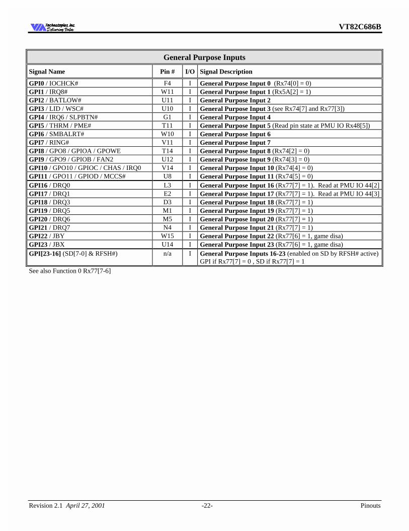
VT82C686B
Revision 2.1 April 27, 2001 -22- Pinouts
7HFKQRORJLHV ,QF'HOLYHULQJ 9DOXH'HOLYHULQJ 9DOXH
General Purpose Inputs
Signal Name Pin # I/O Signal Description
GPI0 / IOCHCK# F4 I General Purpose Input 0 (Rx74[0] = 0) GPI1 / IRQ8# W11 I General Purpose Input 1 (Rx5A[2] = 1) GPI2 / BATLOW# U11 I General Purpose Input 2 GPI3 / LID / WSC# U10 I General Purpose Input 3 (see Rx74[7] and Rx77[3]) GPI4 / IRQ6 / SLPBTN# G1 I General Purpose Input 4 GPI5 / THRM / PME# T11 I General Purpose Input 5 (Read pin state at PMU IO Rx48[5]) GPI6 / SMBALRT# W10 I General Purpose Input 6 GPI7 / RING# V11 I General Purpose Input 7 GPI8 / GPO8 / GPIOA / GPOWE T14 I General Purpose Input 8 (Rx74[2] = 0) GPI9 / GPO9 / GPIOB / FAN2 U12 I General Purpose Input 9 (Rx74[3] = 0) GPI10 / GPO10 / GPIOC / CHAS / IRQ0 V14 I General Purpose Input 10 (Rx74[4] = 0) GPI11 / GPO11 / GPIOD / MCCS# U8 I General Purpose Input 11 (Rx74[5] = 0) GPI16 / DRQ0 L3 I General Purpose Input 16 (Rx77[7] = 1). Read at PMU IO 44[2] GPI17 / DRQ1 E2 I General Purpose Input 17 (Rx77[7] = 1). Read at PMU IO 44[3] GPI18 / DRQ3 D3 I General Purpose Input 18 (Rx77[7] = 1) GPI19 / DRQ5 M1 I General Purpose Input 19 (Rx77[7] = 1) GPI20 / DRQ6 M5 I General Purpose Input 20 (Rx77[7] = 1) GPI21 / DRQ7 N4 I General Purpose Input 21 (Rx77[7] = 1) GPI22 / JBY W15 I General Purpose Input 22 (Rx77[6] = 1, game disa) GPI23 / JBX U14 I General Purpose Input 23 (Rx77[6] = 1, game disa) GPI[23-16] (SD[7-0] & RFSH#) n/a I General Purpose Inputs 16-23 (enabled on SD by RFSH# active)
GPI if Rx77[7] = 0 , SD if Rx77[7] = 1 See also Function 0 Rx77[7-6]
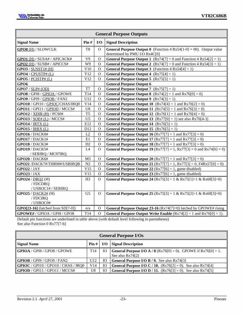
VT82C686B
Revision 2.1 April 27, 2001 -23- Pinouts
7HFKQRORJLHV ,QF'HOLYHULQJ 9DOXH'HOLYHULQJ 9DOXH
General Purpose Outputs
Signal Name Pin # I/O Signal Description
GPO0 (H) / SLOWCLK T8 O General Purpose Output 0 (Function 4 Rx54[1-0] = 00). Output value determined by PMU I/O Rx4C[0]
GPO1 (H) / SUSA# / APICACK# V9 O General Purpose Output 1 (Rx74[7] = 0 and Function 4 Rx54[2] = 1) GPO2 (H) / SUSB# / APICCS# W9 O General Purpose Output 2 (Rx74[7] = 0 and Function 4 Rx54[3] = 1) GPO3 / SUSST1# (H) V10 O General Purpose Output 3 (Function 4 Rx54[4] = 1) GPO4 / CPUSTP# (L) Y12 O General Purpose Output 4 (Rx75[4] = 1) GPO5 / PCISTP# (L) V12 O General Purpose Output 5 (Rx75[5] = 1) GPO6 General Purpose Output 6 GPO7 / SLP# (OD) T7 O General Purpose Output 7 (Rx75[7] = 1) GPO8 / GPI8 / GPIOA / GPOWE T14 O General Purpose Output 8 (Rx74[2] = 1 and Rx76[0] = 0) GPO9 / GPI9 / GPIOB / FAN2 U12 O General Purpose Output 9 (Rx74[3] = 1) GPO10 / GPI10 / GPIOC/CHAS/IRQ0 V14 O General Purpose Output 10 (Rx74[4] = 1 and Rx76[2] = 0) GPO11 / GPI11 / GPIOD / MCCS# U8 O General Purpose Output 11 (Rx74[5] = 1 and Rx76[3] = 0) GPO12 / XDIR (H) / PCS0# T5 O General Purpose Output 12 (Rx76[1] = 1 and Rx76[4] = 0) GPO13 / SOE# (L) / MCCS# U5 O General Purpose Output 13 (Rx77[0] = 1) see also Rx76[4-3] GPO14 / IRTX (L) E12 O General Purpose Output 14 (Rx76[5] = 1) GPO15 / IRRX (L) D12 O General Purpose Output 15 (Rx76[5] = 1) GPO16 / DACK0# L2 O General Purpose Output 16 (Rx77[7] = 1 and Rx77[3] = 0) GPO17 / DACK1# E1 O General Purpose Output 17 (Rx77[7] = 1 and Rx77[3] = 0) GPO18 / DACK3# D2 O General Purpose Output 18 (Rx77[7] = 1 and Rx77[3] = 0) GPO19 / DACK5# / SERIRQ / MC97IRQ
L4 O General Purpose Output 19 (Rx77[7] = 1, Rx77[3] = 0 and Rx74[6] = 0)
GPO20 / DACK6# M3 O General Purpose Output 20 (Rx77[7] = 1 and Rx77[3] = 0) GPO21 /DACK7#/THRM#/USBIRQB N2 O General Purpose Output 21 (Rx77[7] = 1, Rx77[3] = 0, F4Rx57[0] = 0) GPO22 / JAY Y15 O General Purpose Output 22 (Rx77[6] = 1, game disabled) GPO23 / JAX V15 O General Purpose Output 23 (Rx77[6] = 1, game disabled) GPO24 / DRQ2 (H) / FDCDRQ / USBOC1# / SERIRQ
H3 O General Purpose Output 24 (Rx75[3] = 1 & Rx75[1]=1 & Rx68[3]=0)
GPO25 / DACK2# (H) / FDCIRQ / USBOC0#
G5 O General Purpose Output 25 (Rx75[3] = 1 & Rx75[2]=1 & Rx68[3]=0)
GPO[23-16] (latched from SD[7-0]) n/a O General Purpose Output 23-16 (Rx74[7]=0) latched by GPOWE# rising GPOWE# / GPIOA / GPI8 / GPO8 T14 O General Purpose Output Write Enable (Rx74[2] = 1 and Rx76[0] = 1). Default pin functions are underlined in table above (with default level following in parentheses) See also Function 0 Rx77[7-6]
General Purpose I/Os
Signal Name Pin # I/O Signal Description
GPIOA / GPI8 / GPO8 / GPOWE T14 IO General Purpose I/O A / 8 (Rx76[0] = 0). GPOWE if Rx76[0] = 1. See also Rx74[2]
GPIOB / GPI9 / GPO9 / FAN2 U12 IO General Purpose I/O B / 9. See also Rx74[3] GPIOC / GPI10 / GPO10 / CHAS / IRQ0 V14 IO General Purpose I/O C / 10. (Rx76[2] = 0). See also Rx74[4] GPIOD / GPI11 / GPO11 / MCCS# U8 IO General Purpose I/O D / 11. (Rx76[3] = 0). See also Rx74[5]
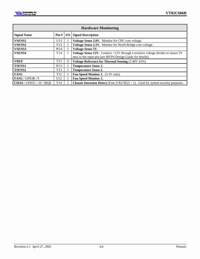
VT82C686B
Revision 2.1 April 27, 2001 -24- Pinouts
7HFKQRORJLHV ,QF'HOLYHULQJ 9DOXH'HOLYHULQJ 9DOXH
Hardware Monitoring
Signal Name Pin # I/O Signal Description
VSENS1 U13 I Voltage Sense 2.0V. Monitor for CPU core voltage. VSENS2 V13 I Voltage Sense 2.5V. Monitor for North Bridge core voltage. VSENS3 W14 I Voltage Sense 5V. VSENS4 Y14 I Voltage Sense 12V. Connect +12V through a resistive voltage divider to insure 5V
max to the input pin (see MVP4 Design Guide for details). VREF T13 O Voltage Reference for Thermal Sensing (2.48V ±5%) TSENS1 W13 I Temperature Sense 1. TSENS2 Y13 I Temperature Sense 2. FAN1 T12 I Fan Speed Monitor 1. (3.3V only) FAN2 / GPIOB / 9 U12 I Fan Speed Monitor 2. CHAS / GPIOC / 10 / IRQ0 V14 I Chassis Intrusion Detect (Func 0 Rx76[2] = 1). Used for system security purposes.
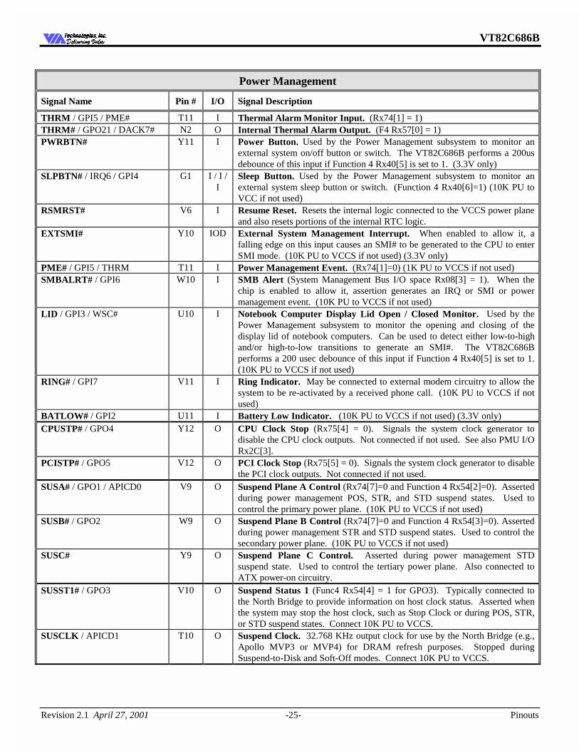
VT82C686B
Revision 2.1 April 27, 2001 -25- Pinouts
7HFKQRORJLHV ,QF'HOLYHULQJ 9DOXH'HOLYHULQJ 9DOXH
Power Management
Signal Name Pin # I/O Signal Description
THRM / GPI5 / PME# T11 I Thermal Alarm Monitor Input. (Rx74[1] = 1) THRM# / GPO21 / DACK7# N2 O Internal Thermal Alarm Output. (F4 Rx57[0] = 1) PWRBTN# Y11 I Power Button. Used by the Power Management subsystem to monitor an
external system on/off button or switch. The VT82C686B performs a 200us debounce of this input if Function 4 Rx40[5] is set to 1. (3.3V only)
SLPBTN# / IRQ6 / GPI4 G1 I / I / I
Sleep Button. Used by the Power Management subsystem to monitor an external system sleep button or switch. (Function 4 Rx40[6]=1) (10K PU to VCC if not used)
RSMRST# V6 I Resume Reset. Resets the internal logic connected to the VCCS power plane and also resets portions of the internal RTC logic.
EXTSMI# Y10 IOD External System Management Interrupt. When enabled to allow it, a falling edge on this input causes an SMI# to be generated to the CPU to enter SMI mode. (10K PU to VCCS if not used) (3.3V only)
PME# / GPI5 / THRM T11 I Power Management Event. (Rx74[1]=0) (1K PU to VCCS if not used) SMBALRT# / GPI6 W10 I SMB Alert (System Management Bus I/O space Rx08[3] = 1). When the
chip is enabled to allow it, assertion generates an IRQ or SMI or power management event. (10K PU to VCCS if not used)
LID / GPI3 / WSC# U10 I Notebook Computer Display Lid Open / Closed Monitor. Used by the Power Management subsystem to monitor the opening and closing of the display lid of notebook computers. Can be used to detect either low-to-high and/or high-to-low transitions to generate an SMI#. The VT82C686B performs a 200 usec debounce of this input if Function 4 Rx40[5] is set to 1. (10K PU to VCCS if not used)
RING# / GPI7 V11 I Ring Indicator. May be connected to external modem circuitry to allow the system to be re-activated by a received phone call. (10K PU to VCCS if not used)
BATLOW# / GPI2 U11 I Battery Low Indicator. (10K PU to VCCS if not used) (3.3V only) CPUSTP# / GPO4 Y12 O CPU Clock Stop (Rx75[4] = 0). Signals the system clock generator to
disable the CPU clock outputs. Not connected if not used. See also PMU I/O Rx2C[3].
PCISTP# / GPO5 V12 O PCI Clock Stop (Rx75[5] = 0). Signals the system clock generator to disable the PCI clock outputs. Not connected if not used.
SUSA# / GPO1 / APICD0 V9 O Suspend Plane A Control (Rx74[7]=0 and Function 4 Rx54[2]=0). Asserted during power management POS, STR, and STD suspend states. Used to control the primary power plane. (10K PU to VCCS if not used)
SUSB# / GPO2 W9 O Suspend Plane B Control (Rx74[7]=0 and Function 4 Rx54[3]=0). Asserted during power management STR and STD suspend states. Used to control the secondary power plane. (10K PU to VCCS if not used)
SUSC# Y9 O Suspend Plane C Control. Asserted during power management STD suspend state. Used to control the tertiary power plane. Also connected to ATX power-on circuitry.
SUSST1# / GPO3 V10 O Suspend Status 1 (Func4 Rx54[4] = 1 for GPO3). Typically connected to the North Bridge to provide information on host clock status. Asserted when the system may stop the host clock, such as Stop Clock or during POS, STR, or STD suspend states. Connect 10K PU to VCCS.
SUSCLK / APICD1 T10 O Suspend Clock. 32.768 KHz output clock for use by the North Bridge (e.g., Apollo MVP3 or MVP4) for DRAM refresh purposes. Stopped during Suspend-to-Disk and Soft-Off modes. Connect 10K PU to VCCS.
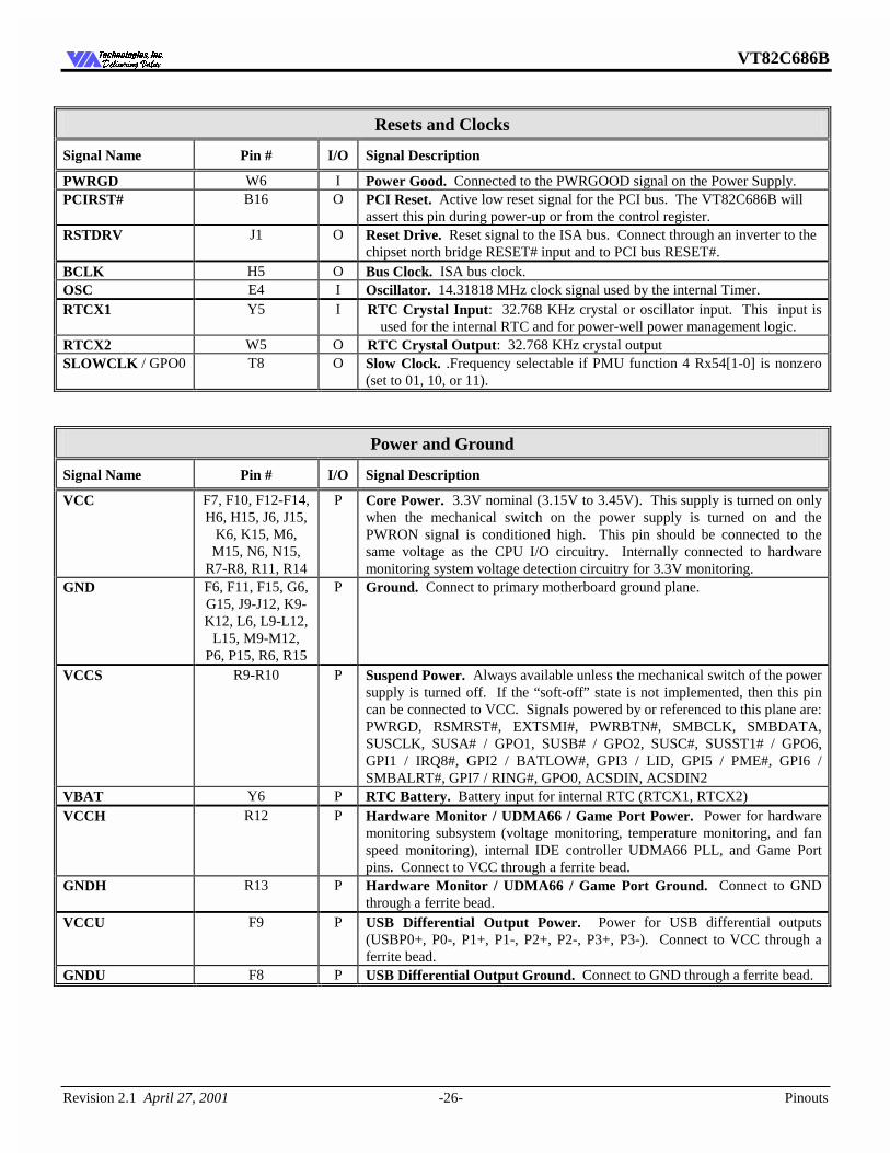
VT82C686B
Revision 2.1 April 27, 2001 -26- Pinouts
7HFKQRORJLHV ,QF'HOLYHULQJ 9DOXH'HOLYHULQJ 9DOXH
Resets and Clocks
Signal Name Pin # I/O Signal Description
PWRGD W6 I Power Good. Connected to the PWRGOOD signal on the Power Supply. PCIRST# B16 O PCI Reset. Active low reset signal for the PCI bus. The VT82C686B will
assert this pin during power-up or from the control register. RSTDRV J1 O Reset Drive. Reset signal to the ISA bus. Connect through an inverter to the
chipset north bridge RESET# input and to PCI bus RESET#. BCLK H5 O Bus Clock. ISA bus clock. OSC E4 I Oscillator. 14.31818 MHz clock signal used by the internal Timer. RTCX1 Y5 I RTC Crystal Input: 32.768 KHz crystal or oscillator input. This input is
used for the internal RTC and for power-well power management logic. RTCX2 W5 O RTC Crystal Output: 32.768 KHz crystal output SLOWCLK / GPO0 T8 O Slow Clock. .Frequency selectable if PMU function 4 Rx54[1-0] is nonzero
(set to 01, 10, or 11).
Power and Ground
Signal Name Pin # I/O Signal Description
VCC F7, F10, F12-F14, H6, H15, J6, J15,
K6, K15, M6, M15, N6, N15,
R7-R8, R11, R14
P Core Power. 3.3V nominal (3.15V to 3.45V). This supply is turned on only when the mechanical switch on the power supply is turned on and the PWRON signal is conditioned high. This pin should be connected to the same voltage as the CPU I/O circuitry. Internally connected to hardware monitoring system voltage detection circuitry for 3.3V monitoring.
GND F6, F11, F15, G6, G15, J9-J12, K9-K12, L6, L9-L12,
L15, M9-M12, P6, P15, R6, R15
P Ground. Connect to primary motherboard ground plane.
VCCS R9-R10 P Suspend Power. Always available unless the mechanical switch of the power supply is turned off. If the “soft-off” state is not implemented, then this pin can be connected to VCC. Signals powered by or referenced to this plane are: PWRGD, RSMRST#, EXTSMI#, PWRBTN#, SMBCLK, SMBDATA, SUSCLK, SUSA# / GPO1, SUSB# / GPO2, SUSC#, SUSST1# / GPO6, GPI1 / IRQ8#, GPI2 / BATLOW#, GPI3 / LID, GPI5 / PME#, GPI6 / SMBALRT#, GPI7 / RING#, GPO0, ACSDIN, ACSDIN2
VBAT Y6 P RTC Battery. Battery input for internal RTC (RTCX1, RTCX2) VCCH R12 P Hardware Monitor / UDMA66 / Game Port Power. Power for hardware
monitoring subsystem (voltage monitoring, temperature monitoring, and fan speed monitoring), internal IDE controller UDMA66 PLL, and Game Port pins. Connect to VCC through a ferrite bead.
GNDH R13 P Hardware Monitor / UDMA66 / Game Port Ground. Connect to GND through a ferrite bead.
VCCU F9 P USB Differential Output Power. Power for USB differential outputs (USBP0+, P0-, P1+, P1-, P2+, P2-, P3+, P3-). Connect to VCC through a ferrite bead.
GNDU F8 P USB Differential Output Ground. Connect to GND through a ferrite bead.
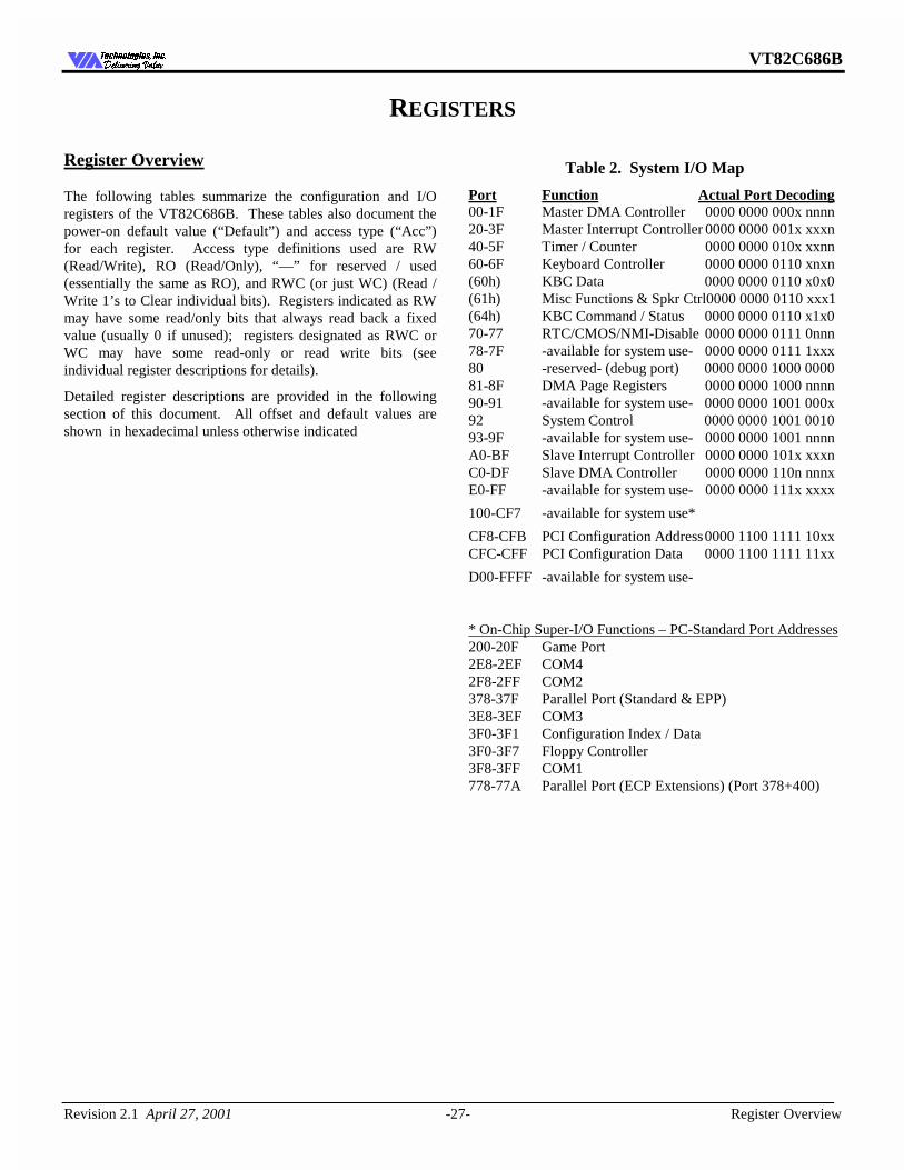
VT82C686B
Revision 2.1 April 27, 2001 -27- Register Overview
7HFKQRORJLHV ,QF'HOLYHULQJ 9DOXH'HOLYHULQJ 9DOXH
REGISTERS
Register Overview
The following tables summarize the configuration and I/O registers of the VT82C686B. These tables also document the power-on default value (“Default”) and access type (“Acc”) for each register. Access type definitions used are RW (Read/Write), RO (Read/Only), “—” for reserved / used (essentially the same as RO), and RWC (or just WC) (Read / Write 1’s to Clear individual bits). Registers indicated as RW may have some read/only bits that always read back a fixed value (usually 0 if unused); registers designated as RWC or WC may have some read-only or read write bits (see individual register descriptions for details).
Detailed register descriptions are provided in the following section of this document. All offset and default values are shown in hexadecimal unless otherwise indicated
Table 2. System I/O Map
Port Function Actual Port Decoding 00-1F Master DMA Controller 0000 0000 000x nnnn 20-3F Master Interrupt Controller 0000 0000 001x xxxn 40-5F Timer / Counter 0000 0000 010x xxnn 60-6F Keyboard Controller 0000 0000 0110 xnxn (60h) KBC Data 0000 0000 0110 x0x0 (61h) Misc Functions & Spkr Ctrl0000 0000 0110 xxx1 (64h) KBC Command / Status 0000 0000 0110 x1x0 70-77 RTC/CMOS/NMI-Disable 0000 0000 0111 0nnn 78-7F -available for system use- 0000 0000 0111 1xxx 80 -reserved- (debug port) 0000 0000 1000 0000 81-8F DMA Page Registers 0000 0000 1000 nnnn 90-91 -available for system use- 0000 0000 1001 000x 92 System Control 0000 0000 1001 0010 93-9F -available for system use- 0000 0000 1001 nnnn A0-BF Slave Interrupt Controller 0000 0000 101x xxxn C0-DF Slave DMA Controller 0000 0000 110n nnnx E0-FF -available for system use- 0000 0000 111x xxxx
100-CF7 -available for system use*
CF8-CFB PCI Configuration Address 0000 1100 1111 10xx CFC-CFF PCI Configuration Data 0000 1100 1111 11xx
D00-FFFF -available for system use-
* On-Chip Super-I/O Functions – PC-Standard Port Addresses 200-20F Game Port 2E8-2EF COM4 2F8-2FF COM2 378-37F Parallel Port (Standard & EPP) 3E8-3EF COM3 3F0-3F1 Configuration Index / Data 3F0-3F7 Floppy Controller 3F8-3FF COM1 778-77A Parallel Port (ECP Extensions) (Port 378+400)
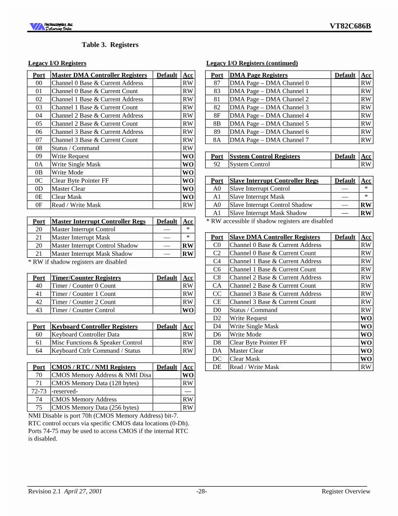
VT82C686B
Revision 2.1 April 27, 2001 -28- Register Overview
7HFKQRORJLHV ,QF'HOLYHULQJ 9DOXH'HOLYHULQJ 9DOXH
Table 3. Registers
Legacy I/O Registers
Port Master DMA Controller Registers Default Acc 00 Channel 0 Base & Current Address RW 01 Channel 0 Base & Current Count RW 02 Channel 1 Base & Current Address RW 03 Channel 1 Base & Current Count RW 04 Channel 2 Base & Current Address RW 05 Channel 2 Base & Current Count RW 06 Channel 3 Base & Current Address RW 07 Channel 3 Base & Current Count RW 08 Status / Command RW 09 Write Request WO 0A Write Single Mask WO 0B Write Mode WO 0C Clear Byte Pointer FF WO 0D Master Clear WO 0E Clear Mask WO 0F Read / Write Mask RW
Port Master Interrupt Controller Regs Default Acc 20 Master Interrupt Control — * 21 Master Interrupt Mask — * 20 Master Interrupt Control Shadow — RW 21 Master Interrupt Mask Shadow — RW
* RW if shadow registers are disabled
Port Timer/Counter Registers Default Acc 40 Timer / Counter 0 Count RW 41 Timer / Counter 1 Count RW 42 Timer / Counter 2 Count RW 43 Timer / Counter Control WO
Port Keyboard Controller Registers Default Acc 60 Keyboard Controller Data RW 61 Misc Functions & Speaker Control RW 64 Keyboard Ctrlr Command / Status RW
Port CMOS / RTC / NMI Registers Default Acc 70 CMOS Memory Address & NMI Disa WO 71 CMOS Memory Data (128 bytes) RW
72-73 -reserved- — 74 CMOS Memory Address RW 75 CMOS Memory Data (256 bytes) RW
NMI Disable is port 70h (CMOS Memory Address) bit-7. RTC control occurs via specific CMOS data locations (0-Dh). Ports 74-75 may be used to access CMOS if the internal RTC is disabled.
Legacy I/O Registers (continued)
Port DMA Page Registers Default Acc 87 DMA Page – DMA Channel 0 RW 83 DMA Page – DMA Channel 1 RW 81 DMA Page – DMA Channel 2 RW 82 DMA Page – DMA Channel 3 RW 8F DMA Page – DMA Channel 4 RW 8B DMA Page – DMA Channel 5 RW 89 DMA Page – DMA Channel 6 RW 8A DMA Page – DMA Channel 7 RW
Port System Control Registers Default Acc 92 System Control RW
Port Slave Interrupt Controller Regs Default Acc A0 Slave Interrupt Control — * A1 Slave Interrupt Mask — * A0 Slave Interrupt Control Shadow — RW A1 Slave Interrupt Mask Shadow — RW
* RW accessible if shadow registers are disabled
Port Slave DMA Controller Registers Default Acc C0 Channel 0 Base & Current Address RW C2 Channel 0 Base & Current Count RW C4 Channel 1 Base & Current Address RW C6 Channel 1 Base & Current Count RW C8 Channel 2 Base & Current Address RW CA Channel 2 Base & Current Count RW CC Channel 3 Base & Current Address RW CE Channel 3 Base & Current Count RW D0 Status / Command RW D2 Write Request WO D4 Write Single Mask WO D6 Write Mode WO D8 Clear Byte Pointer FF WO DA Master Clear WO DC Clear Mask WO DE Read / Write Mask RW
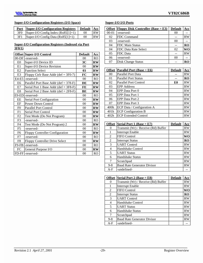
VT82C686B
Revision 2.1 April 27, 2001 -29- Register Overview
7HFKQRORJLHV ,QF'HOLYHULQJ 9DOXH'HOLYHULQJ 9DOXH
Super-I/O Configuration Registers (I/O Space)
Port Super-I/O Configuration Registers Default Acc 3F0 Super-I/O Config Index (Rx85[1]=1) 00 RW 3F1 Super-I/O Config Data (Rx85[1]=1) 00 RW
Super-I/O Configuration Registers (Indexed via Port 3F0/1)
Offset Super-I/O Control Default Acc 00-DF -reserved- 00 RO
E0 Super-I/O Device ID 3C RW E1 Super-I/O Device Revision 00 RW E2 Function Select 03 RW E3 Floppy Ctrlr Base Addr (def = 3F0-7) FC RW
E4-E5 -reserved- 00 RO E6 Parallel Port Base Addr (def = 378-F) DE RW E7 Serial Port 1 Base Addr (def = 3F8-F) FE RW E8 Serial Port 2 Base Addr (def = 2F8-F) BE RW
E9-ED -reserved- 00 RO EE Serial Port Configuration 00 RW EF Power Down Control 00 RW F0 Parallel Port Control 00 RW F1 Serial Port Control 00 RW F2 Test Mode (Do Not Program) 00 RW F3 -reserved- 00 RO F4 Test Mode (Do Not Program) 2 00 RW F5 -reserved- 00 RO F6 Floppy Controller Configuration 00 RW F7 -reserved- 00 RO F8 Floppy Controller Drive Select 00 RW
F9-FB -reserved- 00 RO FC General Purpose I/O 00 RW
FD-FF -reserved- 00 RO
Super-I/O I/O Ports
Offset Floppy Disk Controller (Base = E3) Default Acc 00-01 -reserved- 00 --
02 FDC Command -- RW 03 -reserved- 00 -- 04 FDC Main Status -- RO 04 FDC Data Rate Select 02 WO 05 FDC Data -- RW 06 -reserved- 00 -- 07 Disk Change Status -- RO
Offset Parallel Port (Base = E6) Default Acc
00 Parallel Port Data -- RW 01 Parallel Port Status -- RO 02 Parallel Port Control E0 RW 03 EPP Address RW 04 EPP Data Port 0 RW 05 EPP Data Port 1 RW 06 EPP Data Port 2 RW 07 EPP Data Port 3 RW
400h ECP Data / Configuration A RW 401h ECP Configuration B RW 402h ECP Extended Control RW
Offset Serial Port 1 (Base = E7) Default Acc
0 Transmit (Wr) / Receive (Rd) Buffer RW 1 Interrupt Enable RW 2 FIFO Control WO 2 Interrupt Status RO 3 UART Control RW 4 Handshake Control RW 5 UART Status RW 6 Handshake Status RW 7 Scratchpad RW
9-8 Baud Rate Generator Divisor RW A-F -undefined- --
Offset Serial Port 2 (Base = E8) Default Acc
0 Transmit (Wr) / Receive (Rd) Buffer RW 1 Interrupt Enable RW 2 FIFO Control WO 2 Interrupt Status RO 3 UART Control RW 4 Handshake Control RW 5 UART Status RW 6 Handshake Status RW 7 Scratchpad RW
9-8 Baud Rate Generator Divisor RW A-F -undefined- --
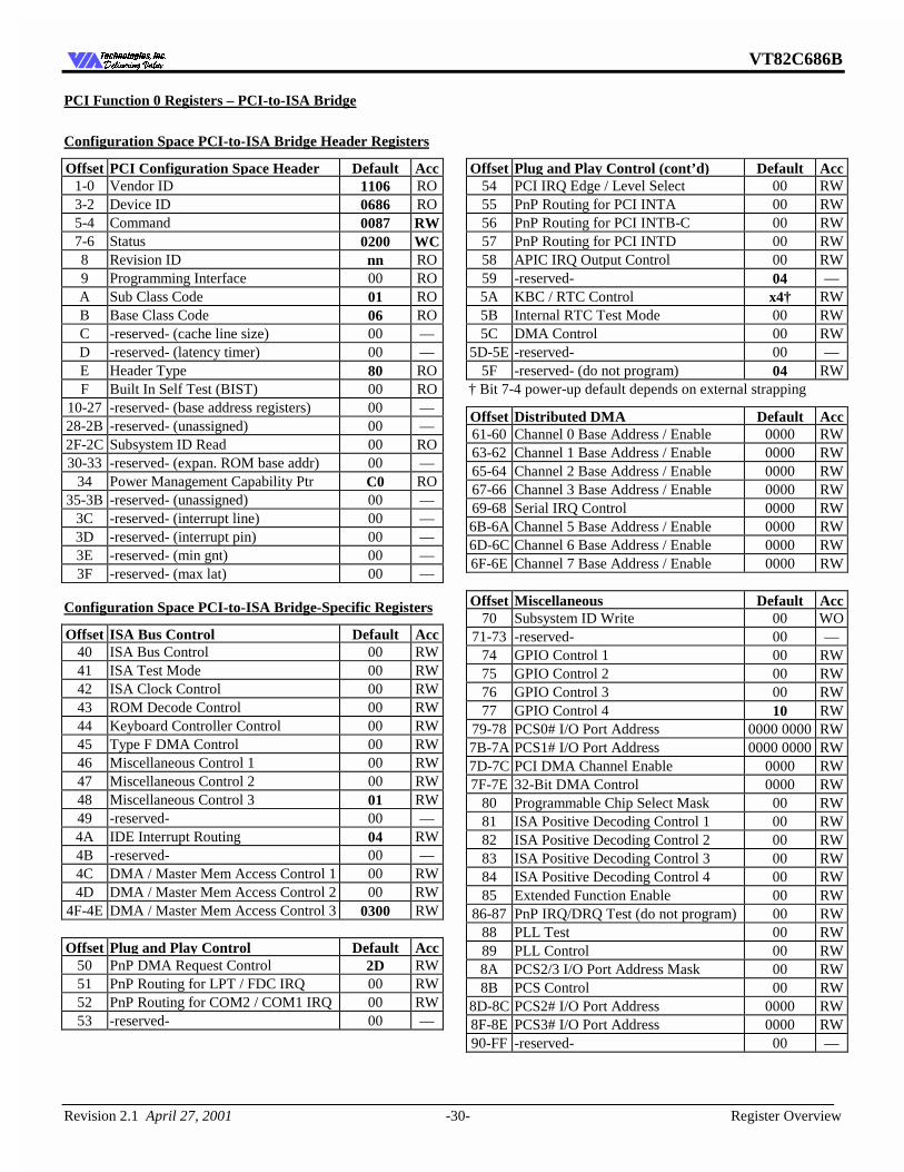
VT82C686B
Revision 2.1 April 27, 2001 -30- Register Overview
7HFKQRORJLHV ,QF'HOLYHULQJ 9DOXH'HOLYHULQJ 9DOXH
PCI Function 0 Registers – PCI-to-ISA Bridge
Configuration Space PCI-to-ISA Bridge Header Registers
Offset PCI Configuration Space Header Default Acc 1-0 Vendor ID 1106 RO 3-2 Device ID 0686 RO 5-4 Command 0087 RW 7-6 Status 0200 WC 8 Revision ID nn RO 9 Programming Interface 00 RO A Sub Class Code 01 RO B Base Class Code 06 RO C -reserved- (cache line size) 00 — D -reserved- (latency timer) 00 — E Header Type 80 RO F Built In Self Test (BIST) 00 RO
10-27 -reserved- (base address registers) 00 — 28-2B -reserved- (unassigned) 00 — 2F-2C Subsystem ID Read 00 RO 30-33 -reserved- (expan. ROM base addr) 00 —
34 Power Management Capability Ptr C0 RO 35-3B -reserved- (unassigned) 00 —
3C -reserved- (interrupt line) 00 — 3D -reserved- (interrupt pin) 00 — 3E -reserved- (min gnt) 00 — 3F -reserved- (max lat) 00 —
Configuration Space PCI-to-ISA Bridge-Specific Registers
Offset ISA Bus Control Default Acc 40 ISA Bus Control 00 RW 41 ISA Test Mode 00 RW 42 ISA Clock Control 00 RW 43 ROM Decode Control 00 RW 44 Keyboard Controller Control 00 RW 45 Type F DMA Control 00 RW 46 Miscellaneous Control 1 00 RW 47 Miscellaneous Control 2 00 RW 48 Miscellaneous Control 3 01 RW 49 -reserved- 00 — 4A IDE Interrupt Routing 04 RW 4B -reserved- 00 — 4C DMA / Master Mem Access Control 1 00 RW 4D DMA / Master Mem Access Control 2 00 RW
4F-4E DMA / Master Mem Access Control 3 0300 RW Offset Plug and Play Control Default Acc
50 PnP DMA Request Control 2D RW 51 PnP Routing for LPT / FDC IRQ 00 RW 52 PnP Routing for COM2 / COM1 IRQ 00 RW 53 -reserved- 00 —
Offset Plug and Play Control (cont’d) Default Acc 54 PCI IRQ Edge / Level Select 00 RW 55 PnP Routing for PCI INTA 00 RW 56 PnP Routing for PCI INTB-C 00 RW 57 PnP Routing for PCI INTD 00 RW 58 APIC IRQ Output Control 00 RW 59 -reserved- 04 — 5A KBC / RTC Control x4† RW 5B Internal RTC Test Mode 00 RW 5C DMA Control 00 RW
5D-5E -reserved- 00 — 5F -reserved- (do not program) 04 RW
† Bit 7-4 power-up default depends on external strapping
Offset Distributed DMA Default Acc 61-60 Channel 0 Base Address / Enable 0000 RW 63-62 Channel 1 Base Address / Enable 0000 RW 65-64 Channel 2 Base Address / Enable 0000 RW 67-66 Channel 3 Base Address / Enable 0000 RW 69-68 Serial IRQ Control 0000 RW 6B-6A Channel 5 Base Address / Enable 0000 RW 6D-6C Channel 6 Base Address / Enable 0000 RW 6F-6E Channel 7 Base Address / Enable 0000 RW Offset Miscellaneous Default Acc
70 Subsystem ID Write 00 WO 71-73 -reserved- 00 —
74 GPIO Control 1 00 RW 75 GPIO Control 2 00 RW 76 GPIO Control 3 00 RW 77 GPIO Control 4 10 RW
79-78 PCS0# I/O Port Address 0000 0000 RW 7B-7A PCS1# I/O Port Address 0000 0000 RW 7D-7C PCI DMA Channel Enable 0000 RW 7F-7E 32-Bit DMA Control 0000 RW
80 Programmable Chip Select Mask 00 RW 81 ISA Positive Decoding Control 1 00 RW 82 ISA Positive Decoding Control 2 00 RW 83 ISA Positive Decoding Control 3 00 RW 84 ISA Positive Decoding Control 4 00 RW 85 Extended Function Enable 00 RW
86-87 PnP IRQ/DRQ Test (do not program) 00 RW 88 PLL Test 00 RW 89 PLL Control 00 RW 8A PCS2/3 I/O Port Address Mask 00 RW 8B PCS Control 00 RW
8D-8C PCS2# I/O Port Address 0000 RW 8F-8E PCS3# I/O Port Address 0000 RW 90-FF -reserved- 00 —
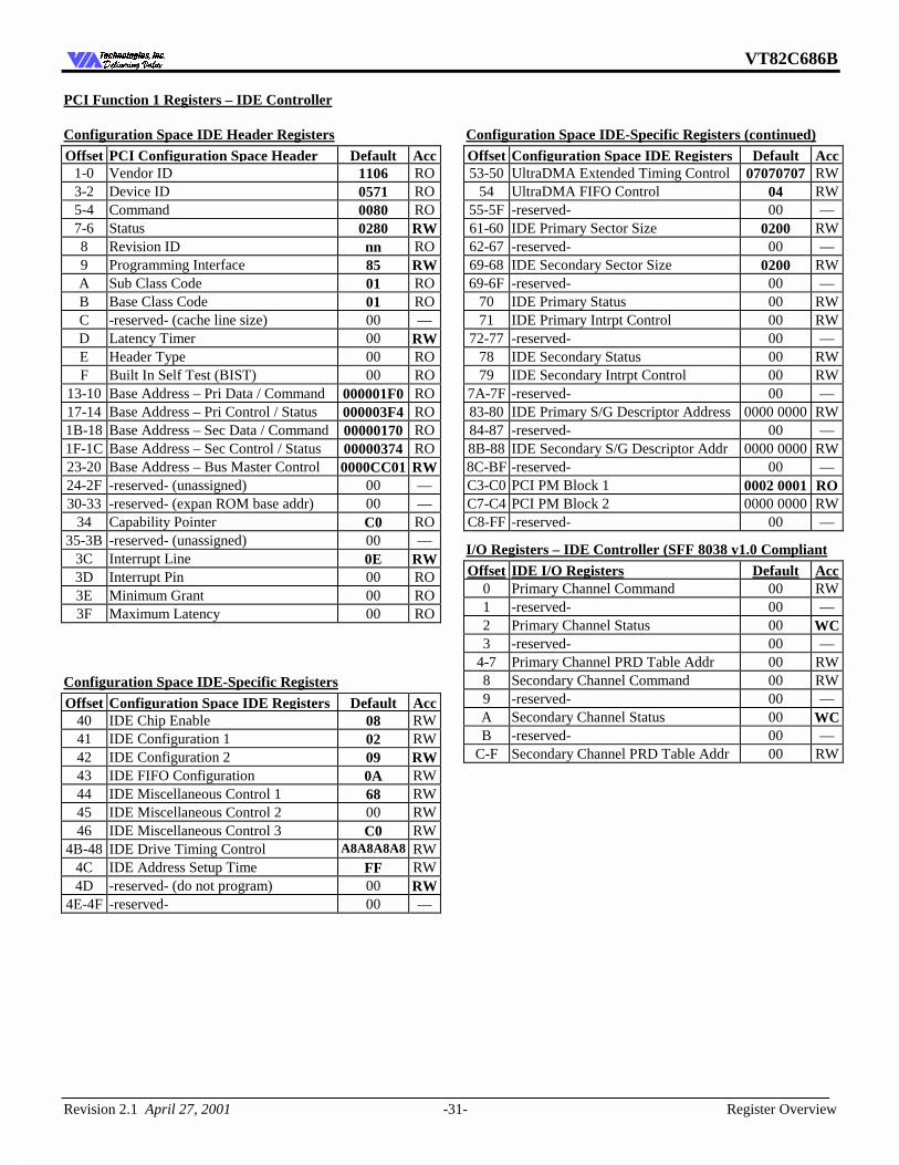
VT82C686B
Revision 2.1 April 27, 2001 -31- Register Overview
7HFKQRORJLHV ,QF'HOLYHULQJ 9DOXH'HOLYHULQJ 9DOXH
PCI Function 1 Registers – IDE Controller
Configuration Space IDE Header Registers
Offset PCI Configuration Space Header Default Acc 1-0 Vendor ID 1106 RO 3-2 Device ID 0571 RO 5-4 Command 0080 RO 7-6 Status 0280 RW 8 Revision ID nn RO 9 Programming Interface 85 RW A Sub Class Code 01 RO B Base Class Code 01 RO C -reserved- (cache line size) 00 — D Latency Timer 00 RW E Header Type 00 RO F Built In Self Test (BIST) 00 RO
13-10 Base Address – Pri Data / Command 000001F0 RO 17-14 Base Address – Pri Control / Status 000003F4 RO 1B-18 Base Address – Sec Data / Command 00000170 RO 1F-1C Base Address – Sec Control / Status 00000374 RO 23-20 Base Address – Bus Master Control 0000CC01 RW 24-2F -reserved- (unassigned) 00 — 30-33 -reserved- (expan ROM base addr) 00 —
34 Capability Pointer C0 RO 35-3B -reserved- (unassigned) 00 —
3C Interrupt Line 0E RW 3D Interrupt Pin 00 RO 3E Minimum Grant 00 RO 3F Maximum Latency 00 RO
Configuration Space IDE-Specific Registers
Offset Configuration Space IDE Registers Default Acc 40 IDE Chip Enable 08 RW 41 IDE Configuration 1 02 RW 42 IDE Configuration 2 09 RW 43 IDE FIFO Configuration 0A RW 44 IDE Miscellaneous Control 1 68 RW 45 IDE Miscellaneous Control 2 00 RW 46 IDE Miscellaneous Control 3 C0 RW
4B-48 IDE Drive Timing Control A8A8A8A8 RW 4C IDE Address Setup Time FF RW 4D -reserved- (do not program) 00 RW
4E-4F -reserved- 00 —
Configuration Space IDE-Specific Registers (continued)
Offset Configuration Space IDE Registers Default Acc 53-50 UltraDMA Extended Timing Control 07070707 RW
54 UltraDMA FIFO Control 04 RW 55-5F -reserved- 00 — 61-60 IDE Primary Sector Size 0200 RW 62-67 -reserved- 00 — 69-68 IDE Secondary Sector Size 0200 RW 69-6F -reserved- 00 —
70 IDE Primary Status 00 RW 71 IDE Primary Intrpt Control 00 RW
72-77 -reserved- 00 — 78 IDE Secondary Status 00 RW 79 IDE Secondary Intrpt Control 00 RW
7A-7F -reserved- 00 — 83-80 IDE Primary S/G Descriptor Address 0000 0000 RW 84-87 -reserved- 00 — 8B-88 IDE Secondary S/G Descriptor Addr 0000 0000 RW 8C-BF -reserved- 00 — C3-C0 PCI PM Block 1 0002 0001 RO C7-C4 PCI PM Block 2 0000 0000 RW C8-FF -reserved- 00 —
I/O Registers – IDE Controller (SFF 8038 v1.0 Compliant
Offset IDE I/O Registers Default Acc 0 Primary Channel Command 00 RW 1 -reserved- 00 — 2 Primary Channel Status 00 WC 3 -reserved- 00 —
4-7 Primary Channel PRD Table Addr 00 RW 8 Secondary Channel Command 00 RW 9 -reserved- 00 — A Secondary Channel Status 00 WC B -reserved- 00 —
C-F Secondary Channel PRD Table Addr 00 RW
VT82C686B
Revision 2.1 April 27, 2001 -32- Register Overview
7HFKQRORJLHV ,QF'HOLYHULQJ 9DOXH'HOLYHULQJ 9DOXH
PCI Function 2 Registers – USB Controller Ports 0-1
Configuration Space USB Header Registers
Offset PCI Configuration Space Header Default Acc 1-0 Vendor ID 1106 RO 3-2 Device ID 3038 RO 5-4 Command 0000 RW 7-6 Status 0210 WC 8 Revision ID nn RO 9 Programming Interface 00 RO A Sub Class Code 03 RO B Base Class Code 0C RO C Cache Line Size 00 RO D Latency Timer 16 RW E Header Type 00 RO F BIST 00 RO
10-1F -reserved- 00 — 23-20 USB I/O Register Base Address 00000301 RW 24-33 -reserved- 00 —
34 USB Power Management Capabilities 80 RO 35-3B -reserved- 00 —
3C Interrupt Line 00 RW 3D Interrupt Pin 04 RO
3E-3F -reserved- 00 —
Configuration Space USB-Specific Registers
Offset USB Control Default Acc 40 USB Miscellaneous Control 1 00 RW 41 USB Miscellaneous Control 2 10 RW 42 USB FIFO Control 00 RW 43 -reserved- 00 —
44-45 -reserved- (test, do not program) RW 46-47 -reserved- (test) RO 48-5F -reserved- 00 —
60 USB Serial Bus Release Number 10 RO 61-7F -reserved- 00 — 83-80 PM Capability 0002 0001 RO
84 PM Capability Status 00 RW 85-BF -reserved- 00 — C1-C0 USB Legacy Support 2000 RW C2-FF -reserved- 00 —
I/O Registers – USB Controller
Offset USB I/O Registers Default Acc 1-0 USB Command 0000 RW 3-2 USB Status 0000 WC 5-4 USB Interrupt Enable 0000 RW 7-6 Frame Number 0000 RW B-8 Frame List Base Address 00000000 RW C Start Of Frame Modify 40 RW
11-10 Port 0 Status / Control 0080 WC 13-12 Port 1 Status / Control 0080 WC 14-1F -reserved- 00 —
PCI Function 3 Registers – USB Controller Ports 2-3
Configuration Space USB Header Registers
Offset PCI Configuration Space Header Default Acc 1-0 Vendor ID 1106 RO 3-2 Device ID 3038 RO 5-4 Command 0000 RW 7-6 Status 0210 WC 8 Revision ID nn RO 9 Programming Interface 00 RO A Sub Class Code 03 RO B Base Class Code 0C RO C Cache Line Size 00 RO D Latency Timer 16 RW E Header Type 00 RO F BIST 00 RO
10-1F -reserved- 00 — 23-20 USB I/O Register Base Address 00000301 RW 24-33 -reserved- 00 —
34 USB Power Management Capabilities 80 RO 35-3B -reserved- 00 —
3C Interrupt Line 00 RW 3D Interrupt Pin 04 RO
3E-3F -reserved- 00 —
Configuration Space USB-Specific Registers
Offset USB Control Default Acc 40 USB Miscellaneous Control 1 00 RW 41 USB Miscellaneous Control 2 10 RW 42 USB FIFO Control 00 RW 43 -reserved- 00 —
44-45 -reserved- (test only, do not program) RW 46-47 -reserved- (test) RO 48-5F -reserved- 00 —
60 USB Serial Bus Release Number 10 RO 61-7F -reserved- 00 — 83-80 PM Capability 0002 0001 RO
84 PM Capability Status 00 RW 85-BF -reserved- 00 — C1-C0 USB Legacy Support 2000 RW C2-FF -reserved- 00 —
I/O Registers - USB Controller
Offset USB I/O Registers Default Acc 1-0 USB Command 0000 RW 3-2 USB Status 0000 WC 5-4 USB Interrupt Enable 0000 RW 7-6 Frame Number 0000 RW B-8 Frame List Base Address 00000000 RW C Start Of Frame Modify 40 RW
11-10 Port 2 Status / Control 0080 WC 13-12 Port 3 Status / Control 0080 WC 14-1F -reserved- 00 —
VT82C686B
Revision 2.1 April 27, 2001 -33- Register Overview
7HFKQRORJLHV ,QF'HOLYHULQJ 9DOXH'HOLYHULQJ 9DOXH
PCI Function 4 Registers - Power Management
Configuration Space Pwr Management Header Registers
Offset PCI Configuration Space Header Default Acc 1-0 Vendor ID 1106 RO 3-2 Device ID 3057 RO 5-4 Command 0000 RO 7-6 Status 0290 WC 8 Revision ID nn RO 9 Programming Interface 00† RO A Sub Class Code 00† RO B Base Class Code 00† RO C Cache Line Size 00 RO D Latency Timer 00 RO E Header Type 00 RO F BIST 00 RO
10-33 -reserved- 00 — 34 Pwr Mgmt Extended Capabilities Ptr 68 RO
35-3F -reserved- 00 — † The default values for these registers may be changed by writing to offsets 61-63h (see below).
Configuration Space Power Management Registers
Offset Power Management Default Acc 40 General Configuration 0 00 RW 41 General Configuration 1 00 RW 42 ACPI Interrupt Select 00 RW 43 Internal Timer Read Test — RO
45-44 Primary Interrupt Channel 0000 RW 47-46 Secondary Interrupt Channel 0000 RW 4B-48 Power Mgmt I/O Base (256 Bytes) 0000 0001 RW
4C Host Bus Power Management Control 00 RW 4D Throttle / Clock Stop Control 00 RW
4E-4F -reserved- 00 — 53-50 GP Timer Control 0000 0000 RW
54 Power Well Control 00 RW 55 USB Wakeup Control 00 RW 56 -reserved- 00 — 57 Miscellaneous Control 00 RW 58 GP2 / GP3 Timer Control 00 RW 59 GP2 Timer 00 RW 5A GP3 Timer 00 RW
5B-60 -reserved- 00 — 61 Read value for Offset 9 (Prog Intfc) 00 WO 62 Read value for Offset A (Sub Class) 00 WO 63 Read value for Offset B (Base Class) 00 WO
64-67 -reserved- 00 — 6B-68 Power Management Capabilities I 0002 0001 RO 6F-6C Power Management Capabilities II 0000 0000 RO 70-7F -reserved- 00 —
Configuration Space Hardware Monitor Registers
Offset System Management Bus Default Acc 71-70 Hardware Mon IO Base (128 Bytes) 0001 RW 72-73 -reserved- 00 —
74 Hardware Monitor Control 00 RW 75-8F -reserved- 00 —
Configuration Space SMBus Registers
Offset System Management Bus Default Acc 93-90 SMBus I/O Base (16 Bytes) 0000 0001 RW 94-D1 -reserved- 00 —
D2 SMBus Host Configuration 00 RW D3 SMBus Host Slave Command 00 RW D4 SMBus Slave Address Shadow Port 1 00 RW D5 SMBus Slave Address Shadow Port 2 00 RW D6 SMBus Revision ID nn RO
D7-FF -reserved- 00 —
VT82C686B
Revision 2.1 April 27, 2001 -34- Register Overview
7HFKQRORJLHV ,QF'HOLYHULQJ 9DOXH'HOLYHULQJ 9DOXH
I/O Space Power Management- Registers
Offset Basic Control / Status Registers Default Acc 1-0 Power Management Status 0000 WC 3-2 Power Management Enable 0000 RW 5-4 Power Management Control 0000 RW 6-7 -reserved- 00 — B-8 Power Management Timer 0000 0000 RW C-F -reserved- 00 —
Offset Processor Registers Default Acc 13-10 Processor and PCI Bus Control 0000 0000 RW
14 Processor LVL2 00 RO 15 Processor LVL3 00 RO
16-1F -reserved- 00 — Offset General Purpose Registers Default Acc 21-20 General Purpose Status 0000 WC 23-22 General Purpose SCI Enable 0000 RW 25-24 General Purpose SMI Enable 0000 RW 26-27 -reserved- 00 — Offset Generic Registers Default Acc 29-28 Global Status 0000 WC 2B-2A Global Enable 0000 RW 2D-2C Global Control 0010 RW
2E -reserved- 00 — 2F SMI Command 00 RW
33-30 Primary Activity Detect Status 0000 0000 WC 37-34 Primary Activity Detect Enable 0000 0000 RW 3B-38 GP Timer Reload Enable 0000 0000 RW 3C-3F -reserved- 00 — Offset General Purpose I/O Registers Default Acc
40 Extended I/O Trap Status 00 WC 41 -reserved- 00 — 42 Extended I/O Trap Enable 00 RW 43 -reserved- 00 — 44 External SMI / GPI Input Value input RO 45 SMI / IRQ / Resume Status 00 RO
46-47 -reserved- 00 — 4B-48 GPI Port Input Value input RO 4F-4C GPO Port Output Value 03FF FFFF RW 50-FF -reserved- 00 —
I/O Space System Management Bus Registers
Offset System Management Bus Default Acc 0 SMBus Host Status 00 WC 1 SMBus Slave Status 00 RW 2 SMBus Host Control 00 RW 3 SMBus Host Command 00 RW 4 SMBus Host Address 00 RW 5 SMBus Host Data 0 00 RW 6 SMBus Host Data 1 00 RW 7 SMBus Block Data 00 RW 8 SMBus Slave Control 00 RW 9 SMBus Shadow Command 00 RO
A-B SMBus Slave Event 0000 RW C-D SMBus Slave Data 0000 RO
0E-53 -reserved- 00 — 54 SMBus Clock Select 00 RW
55-FF -reserved- 00 —
VT82C686B
Revision 2.1 April 27, 2001 -35- Register Overview
7HFKQRORJLHV ,QF'HOLYHULQJ 9DOXH'HOLYHULQJ 9DOXH
I/O Space Hardware Monitor Registers
Offset Hardware Monitor Default Acc 00-3F Value RAM 00-12 -reserved- 00 —
13 Analog Data 15-8 00 RW 14 Analog Data 7-0 00 RW 15 Digital Data 7-0 00 RW 16 Channel Counter 00 RW 17 Data Valid & Channel Indicators 00 RW
18-1F -reserved- 00 — 20 TSENS1 (W13) Temp Reading 00 RW 21 TSENS2 (Y13) Temp Reading 00 RW 22 VSENS1 (U13) Voltage Reading 00 RW 23 VSENS2 (V13) Voltage Reading 00 RW 24 Internal Core VCC Voltage Reading 00 RW 25 VSENS3 (W14) Voltage Reading 00 RW 26 VSENS4 (Y14) Voltage Reading 00 RW 27 -reserved- (-12V Voltage Reading) 00 — 28 -reserved- (-5V Voltage Reading) 00 — 29 FAN1 (T12) Count Reading 00 RW 2A FAN2 (U12) Count Reading 00 RW 2B VSENS1 (CPU) Voltage High Limit 00 RW 2C VSENS1 (CPU) Voltage Low Limit 00 RW 2D VSENS2 (NB) Voltage High Limit 00 RW 2E VSENS2 (NB) Voltage Low Limit 00 RW 2F Internal Core VCC High Limit 00 RW 30 Internal Core VCC Low Limit 00 RW 31 VSENS3 (5V) Voltage High Limit 00 RW 32 VSENS3 (5V) Voltage Low Limit 00 RW 33 VSENS4 (12V) Voltage High Limit 00 RW 34 VSENS4 (12V) Voltage Low Limit 00 RW 35 -reserved- (-12V Sense High Limit) 00 — 36 -reserved- (-12V Sense Low Limit) 00 — 37 -reserved- (-5V Sense High Limit) 00 — 38 -reserved- (-5V Sense Low Limit) 00 — 39 TSENS1 Hot High Limit 00 RW 3A TSENS1 Hot Hysteresis Lo Lim 00 RW 3B FAN1 Fan Count Limit 00 RW 3C FAN2 Fan Count Limit 00 RW 3D TSENS2 Hot High Limit 00 RW 3E TSENS2 Hot Hysteresis Lo Lim 00 RW 3F Stepping ID Number 00 RW
Offset Hardware Monitor (continued) Default Acc 40 Hardware Monitor Configuration 08 RW 41 Hardware Monitor Interrupt Status 1 00 RO 42 Hardware Monitor Interrupt Status 2 00 RO 43 Hardware Monitor Interrupt Mask 1 00 RW 44 Hardware Monitor Interrupt Mask 2 00 RW
45-46 -reserved- 00 — 47 Hardware Monitor Fan Configuration 50 RW 48 -reserved- 00 — 49 HW Mon Temp Value Lo-Order Bits 00 RW 4A -reserved- 00 — 4B Temperature Interrupt Configuration 15 RW
4C-FF -reserved- 00 —
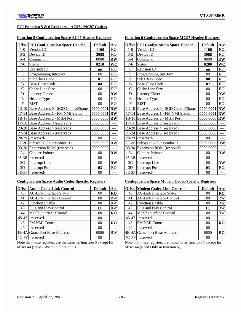
VT82C686B
Revision 2.1 April 27, 2001 -36- Register Overview
7HFKQRORJLHV ,QF'HOLYHULQJ 9DOXH'HOLYHULQJ 9DOXH
PCI Function 5 & 6 Registers – AC97 / MC97 Codecs
Function 5 Configuration Space AC97 Header Registers
Offset PCI Configuration Space Header Default Acc 1-0 Vendor ID 1106 RO 3-2 Device ID 3058 RO 5-4 Command 0000 RW 7-6 Status 0210 WC 8 Revision ID nn RO 9 Programming Interface 00 RO A Sub Class Code 01 RO B Base Class Code 04 RO C Cache Line Size 00 RO D Latency Timer 00 RW E Header Type 00 RO F BIST 00 RO
13-10 Base Address 0 - SGD Control/Status 0000 0001 RW 17-14 Base Address 1 - FM NMI Status 0000 0001 RW 1B-18 Base Address 2 - MIDI Port 0000 0000 RW 1F-1C Base Address 3 (reserved) 0000 0000 — 23-20 Base Address 4 (reserved) 0000 0000 — 27-24 Base Address 5 (reserved) 0000 0000 — 28-29 -reserved- 00 — 2F-2C Subsys ID / SubVendor ID 0000 0000 RW 33-30 Expansion ROM (reserved) 0000 0000 —
34 Capture Pointer 00 RW 35-3B -reserved- 00 —
3C Interrupt Line 00 RW 3D Interrupt Pin 03 RO
3E-3F -reserved- 00 —
Configuration Space Audio Codec-Specific Registers
Offset Audio Codec Link Control Default Acc 40 AC-Link Interface Status 00 RO 41 AC-Link Interface Control 00 RW 42 Function Enable 00 RW 43 Plug and Play Control 1C RW 44 MC97 Interface Control 00 RO
45-47 -reserved- 00 — 48 FM NMI Control 00 RO 49 -reserved- 00 —
4B-4A Game Port Base Address 0000 RW 4C-FF -reserved- 00 — Note that these registers are the same as function 6 except for offset 44 (Read / Write in function 6)
Function 6 Configuration Space MC97 Header Registers
Offset PCI Configuration Space Header Default Acc 1-0 Vendor ID 1106 RO 3-2 Device ID 3068 RO 5-4 Command 0000 RW 7-6 Status 0200 WC 8 Revision ID nn RO 9 Programming Interface 00 RO A Sub Class Code 80 RO B Base Class Code 07 RO C Cache Line Size 00 RO D Latency Timer 00 RW E Header Type 00 RO F BIST 00 RO
13-10 Base Address 0 - SGD Control/Status 0000 0001 RW 17-14 Base Address 1 - FM NMI Status 0000 0001 RW 1B-18 Base Address 2 - MIDI Port 0000 0000 RW 1F-1C Base Address 3 (reserved) 0000 0000 — 23-20 Base Address 4 (reserved) 0000 0000 — 27-24 Base Address 5 (reserved) 0000 0000 — 28-29 -reserved- 00 — 2F-2C Subsys ID / SubVendor ID 0000 0000 RW 33-30 Expansion ROM (reserved) 0000 0000 —
34 Capture Pointer 00 RW 35-3B -reserved- 00 —
3C Interrupt Line 00 RW 3D Interrupt Pin 03 RO
3E-3F -reserved- 00 —
Configuration Space Modem Codec-Specific Registers
Offset Modem Codec Link Control Default Acc 40 AC-Link Interface Status 00 RO 41 AC-Link Interface Control 00 RW 42 Function Enable 00 RW 43 Plug and Play Control 1C RW 44 MC97 Interface Control 00 RW
45-47 -reserved- 00 — 48 FM NMI Control 00 RO 49 -reserved- 00 —
4B-4A Game Port Base Address 0000 RO 4C-FF -reserved- 00 — Note that these registers are the same as function 5 except for offset 44 (Read Only in function 5)
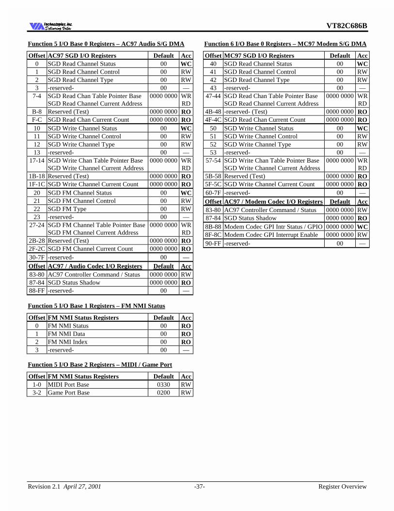
VT82C686B
Revision 2.1 April 27, 2001 -37- Register Overview
7HFKQRORJLHV ,QF'HOLYHULQJ 9DOXH'HOLYHULQJ 9DOXH
Function 5 I/O Base 0 Registers – AC97 Audio S/G DMA
Offset AC97 SGD I/O Registers Default Acc 0 SGD Read Channel Status 00 WC 1 SGD Read Channel Control 00 RW 2 SGD Read Channel Type 00 RW 3 -reserved- 00 —
7-4 SGD Read Chan Table Pointer Base SGD Read Channel Current Address
0000 0000 WR RD
B-8 Reserved (Test) 0000 0000 RO F-C SGD Read Chan Current Count 0000 0000 RO 10 SGD Write Channel Status 00 WC 11 SGD Write Channel Control 00 RW 12 SGD Write Channel Type 00 RW 13 -reserved- 00 —
17-14 SGD Write Chan Table Pointer Base SGD Write Channel Current Address
0000 0000 WR RD
1B-18 Reserved (Test) 0000 0000 RO 1F-1C SGD Write Channel Current Count 0000 0000 RO
20 SGD FM Channel Status 00 WC 21 SGD FM Channel Control 00 RW 22 SGD FM Type 00 RW 23 -reserved- 00 —
27-24 SGD FM Channel Table Pointer Base SGD FM Channel Current Address
0000 0000 WR RD
2B-28 Reserved (Test) 0000 0000 RO 2F-2C SGD FM Channel Current Count 0000 0000 RO 30-7F -reserved- 00 — Offset AC97 / Audio Codec I/O Registers Default Acc 83-80 AC97 Controller Command / Status 0000 0000 RW 87-84 SGD Status Shadow 0000 0000 RO 88-FF -reserved- 00 —
Function 5 I/O Base 1 Registers – FM NMI Status
Offset FM NMI Status Registers Default Acc 0 FM NMI Status 00 RO 1 FM NMI Data 00 RO 2 FM NMI Index 00 RO 3 -reserved- 00 —
Function 5 I/O Base 2 Registers – MIDI / Game Port
Offset FM NMI Status Registers Default Acc 1-0 MIDI Port Base 0330 RW 3-2 Game Port Base 0200 RW
Function 6 I/O Base 0 Registers – MC97 Modem S/G DMA
Offset MC97 SGD I/O Registers Default Acc 40 SGD Read Channel Status 00 WC 41 SGD Read Channel Control 00 RW 42 SGD Read Channel Type 00 RW 43 -reserved- 00 —
47-44 SGD Read Chan Table Pointer Base SGD Read Channel Current Address
0000 0000 WR RD
4B-48 -reserved- (Test) 0000 0000 RO 4F-4C SGD Read Chan Current Count 0000 0000 RO
50 SGD Write Channel Status 00 WC 51 SGD Write Channel Control 00 RW 52 SGD Write Channel Type 00 RW 53 -reserved- 00 —
57-54 SGD Write Chan Table Pointer Base SGD Write Channel Current Address
0000 0000 WR RD
5B-58 Reserved (Test) 0000 0000 RO 5F-5C SGD Write Channel Current Count 0000 0000 RO 60-7F -reserved- 00 — Offset AC97 / Modem Codec I/O Registers Default Acc 83-80 AC97 Controller Command / Status 0000 0000 RW 87-84 SGD Status Shadow 0000 0000 RO 8B-88 Modem Codec GPI Intr Status / GPIO 0000 0000 WC 8F-8C Modem Codec GPI Interrupt Enable 0000 0000 RW 90-FF -reserved- 00 —
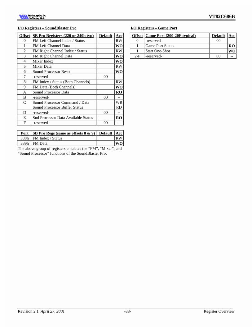
VT82C686B
Revision 2.1 April 27, 2001 -38- Register Overview
7HFKQRORJLHV ,QF'HOLYHULQJ 9DOXH'HOLYHULQJ 9DOXH
I/O Registers – SoundBlaster Pro
Offset SB Pro Registers (220 or 240h typ) Default Acc 0 FM Left Channel Index / Status RW 1 FM Left Channel Data WO 2 FM Right Channel Index / Status RW 3 FM Right Channel Data WO 4 Mixer Index WO 5 Mixer Data RW 6 Sound Processor Reset WO 7 -reserved- 00 -- 8 FM Index / Status (Both Channels) RW 9 FM Data (Both Channels) WO A Sound Processor Data RO B -reserved- 00 -- C Sound Processor Command / Data
Sound Processor Buffer Status WR
RD D -reserved- 00 -- E Snd Processor Data Available Status RO F -reserved- 00 --
Port SB Pro Regs (same as offsets 8 & 9) Default Acc 388h FM Index / Status RW 389h FM Data WO
The above group of registers emulates the “FM”, “Mixer”, and “Sound Processor” functions of the SoundBlaster Pro.
I/O Registers – Game Port
Offset Game Port (200-20F typical) Default Acc 0 -reserved- 00 -- 1 Game Port Status RO 1 Start One-Shot WO
2-F -reserved- 00 --
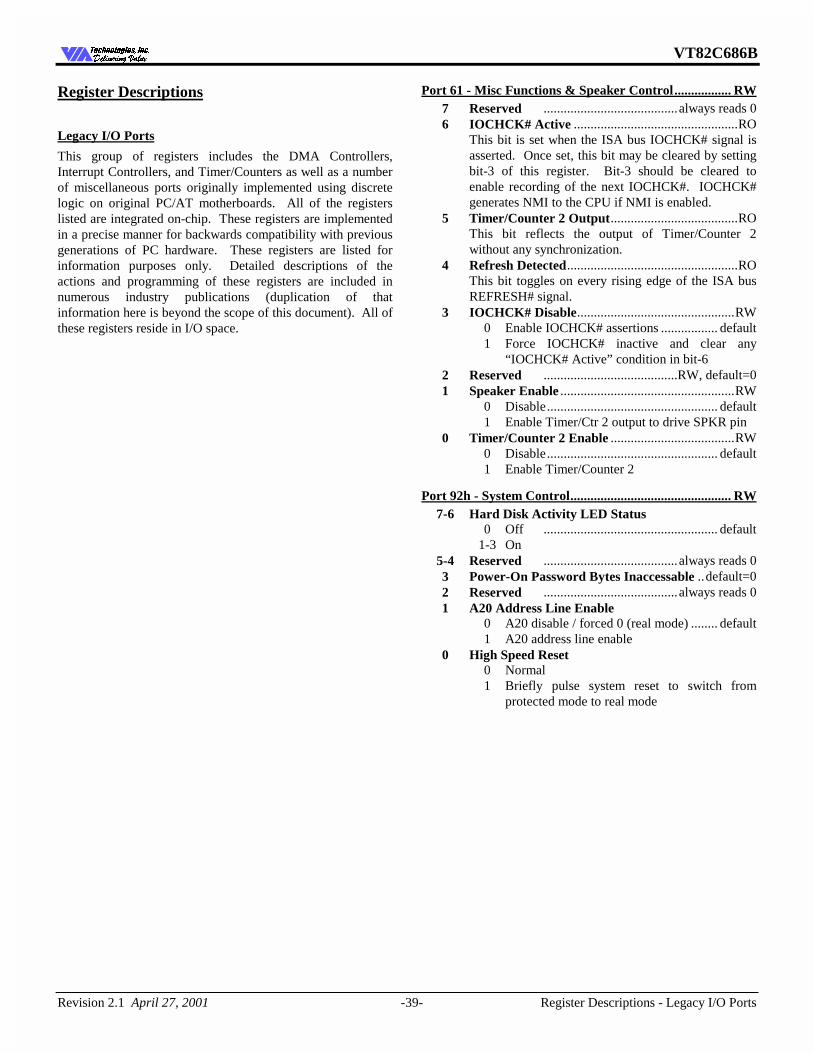
VT82C686B
Revision 2.1 April 27, 2001 -39- Register Descriptions - Legacy I/O Ports
7HFKQRORJLHV ,QF'HOLYHULQJ 9DOXH'HOLYHULQJ 9DOXH
Register Descriptions
Legacy I/O Ports
This group of registers includes the DMA Controllers, Interrupt Controllers, and Timer/Counters as well as a number of miscellaneous ports originally implemented using discrete logic on original PC/AT motherboards. All of the registers listed are integrated on-chip. These registers are implemented in a precise manner for backwards compatibility with previous generations of PC hardware. These registers are listed for information purposes only. Detailed descriptions of the actions and programming of these registers are included in numerous industry publications (duplication of that information here is beyond the scope of this document). All of these registers reside in I/O space.
Port 61 - Misc Functions & Speaker Control................. RW 7 Reserved ........................................always reads 0 6 IOCHCK# Active .................................................RO This bit is set when the ISA bus IOCHCK# signal is
asserted. Once set, this bit may be cleared by setting bit-3 of this register. Bit-3 should be cleared to enable recording of the next IOCHCK#. IOCHCK# generates NMI to the CPU if NMI is enabled.
5 Timer/Counter 2 Output......................................RO This bit reflects the output of Timer/Counter 2
without any synchronization. 4 Refresh Detected...................................................RO This bit toggles on every rising edge of the ISA bus
REFRESH# signal. 3 IOCHCK# Disable...............................................RW 0 Enable IOCHCK# assertions ................. default 1 Force IOCHCK# inactive and clear any
“IOCHCK# Active” condition in bit-6 2 Reserved ........................................RW, default=0 1 Speaker Enable ....................................................RW 0 Disable................................................... default 1 Enable Timer/Ctr 2 output to drive SPKR pin 0 Timer/Counter 2 Enable .....................................RW 0 Disable................................................... default 1 Enable Timer/Counter 2
Port 92h - System Control................................................ RW 7-6 Hard Disk Activity LED Status 0 Off .................................................... default 1-3 On 5-4 Reserved ........................................always reads 0 3 Power-On Password Bytes Inaccessable ..default=0 2 Reserved ........................................always reads 0 1 A20 Address Line Enable 0 A20 disable / forced 0 (real mode) ........ default 1 A20 address line enable 0 High Speed Reset 0 Normal 1 Briefly pulse system reset to switch from
protected mode to real mode
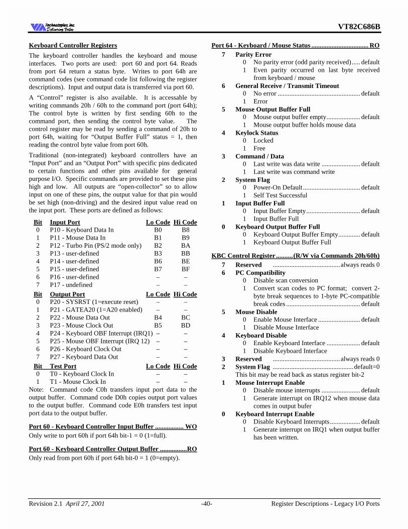
VT82C686B
Revision 2.1 April 27, 2001 -40- Register Descriptions - Legacy I/O Ports
7HFKQRORJLHV ,QF'HOLYHULQJ 9DOXH'HOLYHULQJ 9DOXH
Keyboard Controller Registers
The keyboard controller handles the keyboard and mouse interfaces. Two ports are used: port 60 and port 64. Reads from port 64 return a status byte. Writes to port 64h are command codes (see command code list following the register descriptions). Input and output data is transferred via port 60.
A “Control” register is also available. It is accessable by writing commands 20h / 60h to the command port (port 64h); The control byte is written by first sending 60h to the command port, then sending the control byte value. The control register may be read by sending a command of 20h to port 64h, waiting for “Output Buffer Full” status = 1, then reading the control byte value from port 60h.
Traditional (non-integrated) keyboard controllers have an “Input Port” and an “Output Port” with specific pins dedicated to certain functions and other pins available for general purpose I/O. Specific commands are provided to set these pins high and low. All outputs are “open-collector” so to allow input on one of these pins, the output value for that pin would be set high (non-driving) and the desired input value read on the input port. These ports are defined as follows:
Bit Input Port Lo Code Hi Code 0 P10 - Keyboard Data In B0 B8 1 P11 - Mouse Data In B1 B9 2 P12 - Turbo Pin (PS/2 mode only) B2 BA 3 P13 - user-defined B3 BB 4 P14 - user-defined B6 BE 5 P15 - user-defined B7 BF 6 P16 - user-defined – – 7 P17 - undefined – –
Bit Output Port Lo Code Hi Code 0 P20 - SYSRST (1=execute reset) – – 1 P21 - GATEA20 (1=A20 enabled) – – 2 P22 - Mouse Data Out B4 BC 3 P23 - Mouse Clock Out B5 BD 4 P24 - Keyboard OBF Interrupt (IRQ1) – – 5 P25 - Mouse OBF Interrupt (IRQ 12) – – 6 P26 - Keyboard Clock Out – – 7 P27 - Keyboard Data Out – –
Bit Test Port Lo Code Hi Code 0 T0 - Keyboard Clock In – – 1 T1 - Mouse Clock In – – Note: Command code C0h transfers input port data to the output buffer. Command code D0h copies output port values to the output buffer. Command code E0h transfers test input port data to the output buffer.
Port 60 - Keyboard Controller Input Buffer ................. WO Only write to port 60h if port 64h bit-1 = 0 (1=full).
Port 60 - Keyboard Controller Output Buffer ................RO Only read from port 60h if port 64h bit-0 = 1 (0=empty).
Port 64 - Keyboard / Mouse Status .................................. RO 7 Parity Error 0 No parity error (odd parity received)..... default 1 Even parity occurred on last byte received
from keyboard / mouse 6 General Receive / Transmit Timeout 0 No error ................................................. default 1 Error 5 Mouse Output Buffer Full 0 Mouse output buffer empty.................... default 1 Mouse output buffer holds mouse data 4 Keylock Status 0 Locked 1 Free 3 Command / Data 0 Last write was data write ....................... default 1 Last write was command write 2 System Flag 0 Power-On Default .................................. default 1 Self Test Successful 1 Input Buffer Full 0 Input Buffer Empty................................ default 1 Input Buffer Full 0 Keyboard Output Buffer Full 0 Keyboard Output Buffer Empty............. default 1 Keyboard Output Buffer Full
KBC Control Register ..........(R/W via Commands 20h/60h) 7 Reserved ........................................always reads 0 6 PC Compatibility 0 Disable scan conversion 1 Convert scan codes to PC format; convert 2-
byte break sequences to 1-byte PC-compatible break codes ............................................ default
5 Mouse Disable 0 Enable Mouse Interface ......................... default 1 Disable Mouse Interface 4 Keyboard Disable 0 Enable Keyboard Interface .................... default 1 Disable Keyboard Interface 3 Reserved ........................................always reads 0 2 System Flag ................................................default=0 This bit may be read back as status register bit-2 1 Mouse Interrupt Enable 0 Disable mouse interrupts ....................... default 1 Generate interrupt on IRQ12 when mouse data
comes in output bufer 0 Keyboard Interrupt Enable 0 Disable Keyboard Interrupts.................. default 1 Generate interrupt on IRQ1 when output buffer
has been written.
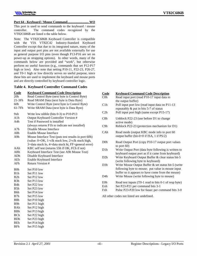
VT82C686B
Revision 2.1 April 27, 2001 -41- Register Descriptions - Legacy I/O Ports
7HFKQRORJLHV ,QF'HOLYHULQJ 9DOXH'HOLYHULQJ 9DOXH
Port 64 - Keyboard / Mouse Command.......................... WO This port is used to send commands to the keyboard / mouse controller. The command codes recognized by the VT82C686B are listed n the table below.
Note: The VT82C686B Keyboard Controller is compatible with the VIA VT82C42 Industry-Standard Keyboard Controller except that due to its integrated nature, many of the input and output port pins are not available externally for use as general purpose I/O pins (even though P13-P16 are set on power-up as strapping options). In other words, many of the commands below are provided and “work”, but otherwise perform no useful function (e.g., commands that set P12-P17 high or low). Also note that setting P10-11, P22-23, P26-27, and T0-1 high or low directly serves no useful purpose, since these bits are used to implement the keyboard and mouse ports and are directly controlled by keyboard controller logic.
Table 4. Keyboard Controller Command Codes
Code Keyboard Command Code Description 20h Read Control Byte (next byte is Control Byte) 21-3Fh Read SRAM Data (next byte is Data Byte) 60h Write Control Byte (next byte is Control Byte) 61-7Fh Write SRAM Data (next byte is Data Byte)
9xh Write low nibble (bits 0-3) to P10-P13 A1h Output Keyboard Controller Version # A4h Test if Password is installed (always returns F1h to indicate not installed) A7h Disable Mouse Interface A8h Enable Mouse Interface A9h Mouse Interface Test (puts test results in port 60h) (value: 0=OK, 1=clk stuck low, 2=clk stuck high, 3=data stuck lo, 4=data stuck hi, FF=general error) AAh KBC self test (returns 55h if OK, FCh if not) ABh Keyboard Interface Test (see A9h Mouse Test) ADh Disable Keyboard Interface AEh Enable Keyboard Interface AFh Return Version #
B0h Set P10 low B1h Set P11 low B2h Set P12 low B3h Set P13 low B4h Set P22 low B5h Set P23 low B6h Set P14 low B7h Set P15 low B8h Set P10 high B9h Set P11 high BAh Set P12 high BBh Set P13 high BCh Set P22 high BDh Set P23 high BEh Set P14 high BFh Set P15 high
Code Keyboard Command Code Description C0h Read input port (read P10-17 input data to the output buffer) C1h Poll input port low (read input data on P11-13 repeatably & put in bits 5-7 of status C2h Poll input port high (same except P15-17)
C8h Unblock P22-23 (use before D1 to change active mode) C9h Reblock P22-23 (protection mechanism for D1)
CAh Read mode (output KBC mode info to port 60 output buffer (bit-0=0 if ISA, 1 if PS/2)
D0h Read Output Port (copy P10-17 output port values to port 60) D1h Write Output Port (data byte following is written to keyboard output port as if it came from keyboard) D2h Write Keyboard Output Buffer & clear status bit-5 (write following byte to keyboard) D3h Write Mouse Output Buffer & set status bit-5 (write following byte to mouse; put value in mouse input buffer so it appears to have come from the mouse) D4h Write Mouse (write following byte to mouse)
E0h Read test inputs (T0-1 read to bits 0-1 of resp byte) Exh Set P23-P21 per command bits 3-1 Fxh Pulse P23-P20 low for 6usec per command bits 3-0
All other codes not listed are undefined.
VT82C686B
Revision 2.1 April 27, 2001 -42- Register Descriptions - Legacy I/O Ports
7HFKQRORJLHV ,QF'HOLYHULQJ 9DOXH'HOLYHULQJ 9DOXH
DMA Controller I/O Registers
Ports 00-0F - Master DMA Controller Channels 0-3 of the Master DMA Controller control System DMA Channels 0-3. There are 16 Master DMA Controller registers:
I/O Address Bits 15-0 Register Name 0000 0000 000x 0000 Ch 0 Base / Current Address RW 0000 0000 000x 0001 Ch 0 Base / Current Count RW 0000 0000 000x 0010 Ch 1 Base / Current Address RW 0000 0000 000x 0011 Ch 1 Base / Current Count RW 0000 0000 000x 0100 Ch 2 Base / Current Address RW 0000 0000 000x 0101 Ch 2 Base / Current Count RW 0000 0000 000x 0110 Ch 3 Base / Current Address RW 0000 0000 000x 0111 Ch 3 Base / Current Count RW 0000 0000 000x 1000 Status / Command RW 0000 0000 000x 1001 Write Request WO 0000 0000 000x 1010 Write Single Mask WO 0000 0000 000x 1011 Write Mode WO 0000 0000 000x 1100 Clear Byte Pointer F/F WO 0000 0000 000x 1101 Master Clear WO 0000 0000 000x 1110 Clear Mask WO 0000 0000 000x 1111 R/W All Mask Bits RW
Ports C0-DF - Slave DMA Controller Channels 0-3 of the Slave DMA Controller control System DMA Channels 4-7. There are 16 Slave DMA Controller registers:
I/O Address Bits 15-0 Register Name 0000 0000 1100 000x Ch 4 Base / Current Address RW 0000 0000 1100 001x Ch 4 Base / Current Count RW 0000 0000 1100 010x Ch 5 Base / Current Address RW 0000 0000 1100 011x Ch 5 Base / Current Count RW 0000 0000 1100 100x Ch 6 Base / Current Address RW 0000 0000 1100 101x Ch 6 Base / Current Count RW 0000 0000 1100 110x Ch 7 Base / Current Address RW 0000 0000 1100 111x Ch 7 Base / Current Count RW 0000 0000 1101 000x Status / Command RW 0000 0000 1101 001x Write Request WO 0000 0000 1101 010x Write Single Mask WO 0000 0000 1101 011x Write Mode WO 0000 0000 1101 100x Clear Byte Pointer F/F WO 0000 0000 1101 101x Master Clear WO 0000 0000 1101 110x Clear Mask WO 0000 0000 1101 111x Read/Write All Mask Bits WO Note that not all bits of the address are decoded.
The Master and Slave DMA Controllers are compatible with the Intel 8237 DMA Controller chip. Detailed description of 8237 DMA controller operation can be obtained from the Intel Peripheral Components Data Book and numerous other industry publications.
Ports 80-8F - DMA Page Registers There are eight DMA Page Registers, one for each DMA channel. These registers provide bits 16-23 of the 24-bit address for each DMA channel (bits 0-15 are stored in registers in the Master and Slave DMA Controllers). They are located at the following I/O Port addresses:
I/O Address Bits 15-0 Register Name 0000 0000 1000 0111 Channel 0 DMA Page (M-0).........RW 0000 0000 1000 0011 Channel 1 DMA Page (M-1).........RW 0000 0000 1000 0001 Channel 2 DMA Page (M-2).........RW 0000 0000 1000 0010 Channel 3 DMA Page (M-3).........RW
0000 0000 1000 1111 Channel 4 DMA Page (S-0) ..........RW 0000 0000 1000 1011 Channel 5 DMA Page (S-1) ..........RW 0000 0000 1000 1001 Channel 6 DMA Page (S-2) ..........RW 0000 0000 1000 1010 Channel 7 DMA Page (S-3) .........RW
DMA Controller Shadow Registers The DMA Controller shadow registers are enabled by setting function 0 Rx77 bit 0. If the shadow registers are enabled, they are read back at the indicated I/O port instead of the standard DMA controller registers (writes are unchanged).
Port 0 –Channel 0 Base Address ...................................... RO Port 1 –Channel 0 Byte Count.......................................... RO Port 2 –Channel 1 Base Address ...................................... RO Port 3 –Channel 1 Byte Count.......................................... RO Port 4 –Channel 2 Base Address ...................................... RO Port 5 –Channel 2 Byte Count.......................................... RO Port 6 –Channel 3 Base Address ...................................... RO Port 7 –Channel 3 Byte Count.......................................... RO
Port 8 –1st Read Channel 0-3 Command Register .......... RO Port 8 –2nd Read Channel 0-3 Request Register.............. RO Port 8 –3rd Read Channel 0 Mode Register ..................... RO Port 8 –4th Read Channel 1 Mode Register ..................... RO Port 8 –5th Read Channel 2 Mode Register ..................... RO Port 8 –6th Read Channel 3 Mode Register ..................... RO
Port F –Channel 0-3 Read All Mask ................................ RO
Port C4 –Channel 5 Base Address.................................... RO Port C6 –Channel 5 Byte Count ....................................... RO Port C8 –Channel 6 Base Address.................................... RO Port CA –Channel 6 Byte Count ...................................... RO Port CC –Channel 7 Base Address................................... RO Port CE –Channel 7 Byte Count ...................................... RO
Port D0 –1st Read Channel 4-7 Command Register........ RO Port D0 –2nd Read Channel 4-7 Request Register........... RO Port D0 –3rd Read Channel 4 Mode Register .................. RO Port D0 –4th Read Channel 5 Mode Register .................. RO Port D0 –5th Read Channel 6 Mode Register .................. RO Port D0 –6th Read Channel 7 Mode Register .................. RO
Port DE –Channel 4-7 Read All Mask............................. RO
VT82C686B
Revision 2.1 April 27, 2001 -43- Register Descriptions - Legacy I/O Ports
7HFKQRORJLHV ,QF'HOLYHULQJ 9DOXH'HOLYHULQJ 9DOXH
Interrupt Controller Registers
Ports 20-21 - Master Interrupt Controller The Master Interrupt Controller controls system interrupt channels 0-7. Two registers control the Master Interrupt Controller. They are:
I/O Address Bits 15-0 Register Name 0000 0000 001x xxx0 Master Interrupt Control RW 0000 0000 001x xxx1 Master Interrupt Mask RW Note that not all bits of the address are decoded.
The Master Interrupt Controller is compatible with the Intel 8259 Interrupt Controller chip. Detailed descriptions of 8259 Interrupt Controller operation can be obtained from the Intel Peripheral Components Data Book and numerous other industry publications.
Ports A0-A1 - Slave Interrupt Controller The Slave Interrupt Controller controls system interrupt channels 8-15. The slave system interrupt controller also occupies two register locations:
I/O Address Bits 15-0 Register Name 0000 0000 101x xxx0 Slave Interrupt Control RW 0000 0000 101x xxx1 Slave Interrupt Mask RW Note that not all address bits are decoded.
The Slave Interrupt Controller is compatible with the Intel 8259 Interrupt Controller chip. Detailed descriptions of 8259 Interrupt Controller operation can be obtained from the Intel Peripheral Components Data Book and numerous other industry publications.
Interrupt Controller Shadow Registers
The following shadow registers are enabled by setting function 0 Rx47[4]. If the shadow registers are enabled, they are read back at the indicated I/O port instead of the standard interrupt controller registers (writes are unchanged).
Port 20 - Master Interrupt Control Shadow ................... RO Port A0 - Slave Interrupt Control Shadow ..................... RO 7 Reserved ........................................always reads 0 6 OCW3 bit 2 (POLL) 5 OCW3 bit 0 (RIS) 4 OCW3 bit 5 (SMM) 3 OCW2 bit 7 (R) 2 ICW4 bit 4 (SFNM) 1 ICW4 bit 1 (AEOI) 0 ICW1 bit 3 (LTIM)
Port 21 - Master Interrupt Mask Shadow....................... RO Port A1 - Slave Interrupt Mask Shadow ........................ RO 7-5 Reserved ........................................always reads 0 4-0 T7-T3 of Interrupt Vector Address
Timer / Counter Registers
Ports 40-43 - Timer / Counter Registers There are 4 Timer / Counter registers:
I/O Address Bits 15-0 Register Name 0000 0000 010x xx00 Timer / Counter 0 Count RW 0000 0000 010x xx01 Timer / Counter 1 Count RW 0000 0000 010x xx10 Timer / Counter 2 Count RW 0000 0000 010x xx11 Timer / Counter Cmd Mode WO Note that not all bits of the address are decoded.
The Timer / Counters are compatible with the Intel 8254 Timer / Counter chip. Detailed descriptions of 8254 Timer / Counter operation can be obtained from the Intel Peripheral Components Data Book and numerous other industry publications.
Timer / Counter Shadow Registers
The following shadow registers are enabled for readback by setting function 0 Rx47[4]. If the shadow registers are enabled, they are read back at the indicated I/O port instead of the standard timer / counter registers (writes are unchanged).
Port 40 – Counter 0 Base Count Value (LSB 1st MSB 2nd)RO Port 41 – Counter 1 Base Count Value (LSB 1st MSB 2nd)RO Port 42 – Counter 2 Base Count Value (LSB 1st MSB 2nd)RO
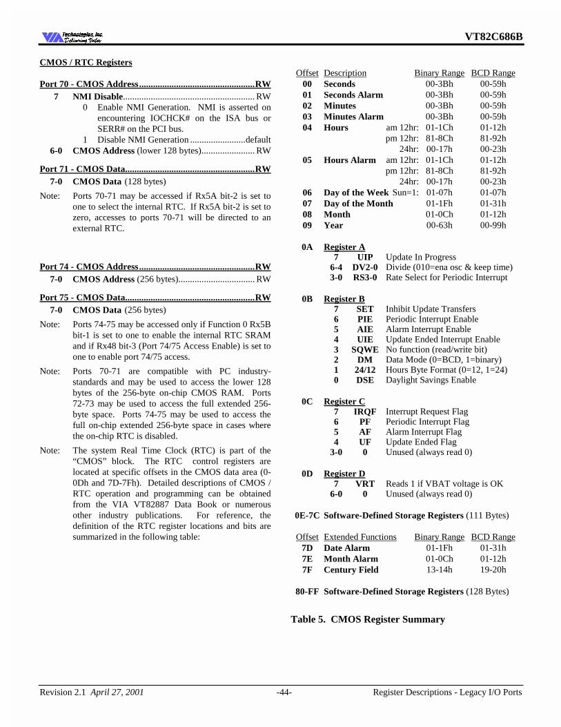
VT82C686B
Revision 2.1 April 27, 2001 -44- Register Descriptions - Legacy I/O Ports
7HFKQRORJLHV ,QF'HOLYHULQJ 9DOXH'HOLYHULQJ 9DOXH
CMOS / RTC Registers
Port 70 - CMOS Address..................................................RW 7 NMI Disable......................................................... RW 0 Enable NMI Generation. NMI is asserted on
encountering IOCHCK# on the ISA bus or SERR# on the PCI bus.
1 Disable NMI Generation ........................default 6-0 CMOS Address (lower 128 bytes)....................... RW
Port 71 - CMOS Data........................................................RW 7-0 CMOS Data (128 bytes)
Note: Ports 70-71 may be accessed if Rx5A bit-2 is set to one to select the internal RTC. If Rx5A bit-2 is set to zero, accesses to ports 70-71 will be directed to an external RTC.
Port 74 - CMOS Address..................................................RW 7-0 CMOS Address (256 bytes)................................. RW
Port 75 - CMOS Data........................................................RW 7-0 CMOS Data (256 bytes)
Note: Ports 74-75 may be accessed only if Function 0 Rx5B bit-1 is set to one to enable the internal RTC SRAM and if Rx48 bit-3 (Port 74/75 Access Enable) is set to one to enable port 74/75 access.
Note: Ports 70-71 are compatible with PC industry-standards and may be used to access the lower 128 bytes of the 256-byte on-chip CMOS RAM. Ports 72-73 may be used to access the full extended 256-byte space. Ports 74-75 may be used to access the full on-chip extended 256-byte space in cases where the on-chip RTC is disabled.
Note: The system Real Time Clock (RTC) is part of the “CMOS” block. The RTC control registers are located at specific offsets in the CMOS data area (0-0Dh and 7D-7Fh). Detailed descriptions of CMOS / RTC operation and programming can be obtained from the VIA VT82887 Data Book or numerous other industry publications. For reference, the definition of the RTC register locations and bits are summarized in the following table:
Offset Description Binary Range BCD Range 00 Seconds 00-3Bh 00-59h 01 Seconds Alarm 00-3Bh 00-59h 02 Minutes 00-3Bh 00-59h 03 Minutes Alarm 00-3Bh 00-59h 04 Hours am 12hr: 01-1Ch 01-12h pm 12hr: 81-8Ch 81-92h 24hr: 00-17h 00-23h 05 Hours Alarm am 12hr: 01-1Ch 01-12h pm 12hr: 81-8Ch 81-92h 24hr: 00-17h 00-23h 06 Day of the Week Sun=1: 01-07h 01-07h 07 Day of the Month 01-1Fh 01-31h 08 Month 01-0Ch 01-12h 09 Year 00-63h 00-99h 0A Register A 7 UIP Update In Progress 6-4 DV2-0 Divide (010=ena osc & keep time) 3-0 RS3-0 Rate Select for Periodic Interrupt 0B Register B 7 SET Inhibit Update Transfers 6 PIE Periodic Interrupt Enable 5 AIE Alarm Interrupt Enable 4 UIE Update Ended Interrupt Enable 3 SQWE No function (read/write bit) 2 DM Data Mode (0=BCD, 1=binary) 1 24/12 Hours Byte Format (0=12, 1=24) 0 DSE Daylight Savings Enable 0C Register C 7 IRQF Interrupt Request Flag 6 PF Periodic Interrupt Flag 5 AF Alarm Interrupt Flag 4 UF Update Ended Flag 3-0 0 Unused (always read 0) 0D Register D 7 VRT Reads 1 if VBAT voltage is OK 6-0 0 Unused (always read 0) 0E-7C Software-Defined Storage Registers (111 Bytes) Offset Extended Functions Binary Range BCD Range 7D Date Alarm 01-1Fh 01-31h 7E Month Alarm 01-0Ch 01-12h 7F Century Field 13-14h 19-20h 80-FF Software-Defined Storage Registers (128 Bytes)
Table 5. CMOS Register Summary
VT82C686B
Revision 2.1 April 27, 2001 -45- Register Descriptions - Super-I/O I/O Ports
7HFKQRORJLHV ,QF'HOLYHULQJ 9DOXH'HOLYHULQJ 9DOXH
Super-I/O Configuration Index / Data Registers
Super-I/O configuration registers are accessed by performing I/O operations to / from an index / data pair of registers in system I/O space at port addresses 3F0h and 3F1h. The configuration registers accessed using this mechanism are used to configure the Super-I/O registers (parallel port, serial ports, IR port, and floppy controller).
Super I/O configuration is accomplished in three steps:
1) Enter configuration mode (set Function 0 Rx85[1] = 1)
2) Configure the chip
a) Write index to port 3F0 b) Read / write data from / to port 3F1 c) Repeat a and b for all desired registers
3) Exit configuration mode (set Function 0 Rx85[1] = 0)
Port 3F0h – Super-I/O Configuration Index...................RW 7-0 Index value Function 0 PCI configuration space register Rx85[1] must be set to 1 to enable access to the Super-I/O configuration registers.
Port 3F1h – Super-I/O Configuration Data ....................RW 7-0 Data value This register shares a port with the Floppy Status Port (which is read only). This port is accessible only when Rx85[1] is set to 1 (the floppy status port is accessed if Rx85[1] = 0).
Super-I/O Configuration Registers
These registers are accessed via the port 3F0 / 3F1 index / data register pair using the indicated index values below
Index E0 – Super-I/O Device ID (3Ch) ............................ RO 7-0 Super-I/O ID ........................................ default = 3Ch
Index E1 – Super-I/O Device Revision (00h) ................... RO 7-0 Super-I/O Revision Code .........................default = 0
Index E2 – Super-I/O Function Select (03h)................... RW 7-5 Reserved ........................................always reads 0 4 Floppy Controller Enable 0 Disable................................................... default 1 Enable 3 Serial Port 2 Enable 0 Disable................................................... default 1 Enable 2 Serial Port 1 Enable 0 Disable................................................... default 1 Enable 1-0 Parallel Port Mode / Enable 00 Unidirectional mode 01 ECP 10 EPP 11 Parallel Port Disable .............................. default
Index E3 – Floppy Controller I/O Base Address (00h).. RW 7-2 I/O Address 9-4 .........................................default = 0 1-0 Must be 0 ..............................................default = 0
Index E6 – Parallel Port I/O Base Address (00h)........... RW 7-0 I/O Address 9-2 .........................................default = 0 If EPP is not enabled, the parallel port can be set to 192 locations on 4-byte boundaries from 100h to 3FCh. If EPP is enabled, the parallel port can be set to 96 locations on 8-byte boundaries from 100h to 3F8h.
Index E7 – Serial Port 1 I/O Base Address (00h) ........... RW 7-1 I/O Address 9-3 .........................................default = 0 0 Must be 0 ..............................................default = 0
Index E8 – Serial Port 2 I/O Base Address (00h) ........... RW 7-1 I/O Address 9-3 .........................................default = 0 0 Must be 0 ..............................................default = 0
VT82C686B
Revision 2.1 April 27, 2001 -46- Register Descriptions - Super-I/O I/O Ports
7HFKQRORJLHV ,QF'HOLYHULQJ 9DOXH'HOLYHULQJ 9DOXH
Index EE – Serial Port Configuration (00h) ...................RW 7 Serial Port 2 High Speed Enable 0 Disable ...................................................default 1 Enable 6 Serial Port 1 High Speed Enable 0 Disable ...................................................default 1 Enable 5-3 Serial Port 2 Mode 000 Standard ................................................default 001 IrDA (HIPSIR) 010 Amplitude shift keyed IR @ 500KHz 011 -reserved- 1xx -reserved- 2 Serial Port 2 Half Duplex 0 Disable ...................................................default 1 Enable 1 Serial Port 2 TX Output Inversion 0 Disable ...................................................default 1 Enable 0 Serial Port 2 RX Input Inversion 0 Disable ...................................................default 1 Enable
Index EF – Power Down Control (00h) ...........................RW 7-6 Reserved ........................................ always reads 0 5 Clock Power Down 0 Normal operation ...................................default 1 Power Down 4 Parallel Port Power Down 0 Normal operation ...................................default 1 Power Down 3 Serial Port 2 Power Down 0 Normal operation ...................................default 1 Power Down 2 Serial Port 1 Power Down 0 Normal operation ...................................default 1 Power Down 1 FDC Power Down 0 Normal operation ...................................default 1 Power Down 0 All Power Down 0 Normal operation ...................................default 1 Power Down All
Index F0 – Parallel Port Control (00h) ........................... RW 7 PS2 Type BiDirectionl Parallel Port 0 Disable................................................... default 1 Enable 6 EPP Direction by Register not by IOW 0 Disable................................................... default 1 Enable 5 EPP+ECP 0 Disable................................................... default 1 Enable 4 EPP Version 0 Version 1.9 ............................................ default 1 Version 1.7 3-0 Reserved ........................................always reads 0
Index F1 – Serial Port Control (00h) .............................. RW 7-6 Reserved ........................................always reads 0 5 IR Loop Back 0 Disable................................................... default 1 Enable 4 Serial Port 2 Power-Down State 0 Normal................................................... default 1 Tristate output in power down mode 3 Serial Port 1 Power-Down State 0 Normal................................................... default 1 Tristate output in power down mode 2 IR Dedicated Pin (IRTX/IRRX) Select 0 IRTX / IRRX Output from Serial Port 2...... def 1 Function 0 Rx76[5] = 0: IRRX output from dedicated pin D12 IRTX output from dedicated pin E12 1-0 Reserved ........................................always reads 0
Index F2 – Test Mode (Do Not Program) ....................... RW
Index F4 – Test Mode (Do Not Program) ....................... RW
VT82C686B
Revision 2.1 April 27, 2001 -47- Register Descriptions - Super-I/O I/O Ports
7HFKQRORJLHV ,QF'HOLYHULQJ 9DOXH'HOLYHULQJ 9DOXH
Index F6 – Floppy Controller Configuration..................RW 7-6 Reserved ........................................ always reads 0 5 Floppy Drive On Parallel Port 0 Parallel Port (SPP) Mode .......................default 1 FDC Mode This bit is used in notebook applications to allow
attachment of an external floppy drive using the parallel port I/O connector:
SPP Mode Pin Type FDC Mode Pin Type STROBE# I/O - n/a
PD0 I/O INDEX# I PD1 I/O TRK00# I PD2 I/O WRTPRT# I PD3 I/O RDATA# I PD4 I/O DSKCHG# I PD5 I/O - n/a PD6 I/O - n/a PD7 I/O - n/a
ACK# I DS1# O BUSY I MTR1# O PE I WDATA# O SLCT I WGATE# O AUTOFD# I/O DRVEN0 O ERROR# I HDSEL# O PINIT# I/O DIR# O SLCTIN# I/O STEP# O 4 3-Mode FDD 0 Disable ...................................................default 1 Enable 3 Reserved ........................................ always reads 0 2 Four Floppy Drive Option 0 Internal 2-Drive Decoder .......................default 1 External 4-Drive Decoder 1 FDC DMA Non-Burst 0 Burst .....................................................default 1 Non-Burst 0 FDC Swap 0 Disable ...................................................default 1 Enable
Index F8 – Floppy Drive Control .................................... RW 7-6 Floppy Drive 3 (see table below) 5-4 Floppy Drive 2 (see table below) 3-2 Floppy Drive 1 (see table below) 1-0 Floppy Drive 0 (see table below) DRVEN1 DRVEN0 00 DRATE0 DENSEL 01 DRATE0 DRATE1 10 DRATE0 DENSEL# 11 DRATE1 DRATE0
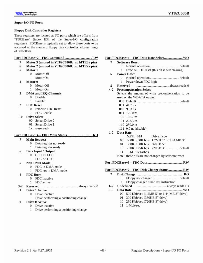
VT82C686B
Revision 2.1 April 27, 2001 -48- Register Descriptions - Super-I/O I/O Ports
7HFKQRORJLHV ,QF'HOLYHULQJ 9DOXH'HOLYHULQJ 9DOXH
Super-I/O I/O Ports
Floppy Disk Controller Registers
These registers are located at I/O ports which are offsets from “FDCBase” (index E3h of the Super-I/O configuration registers). FDCBase is typically set to allow these ports to be accessed at the standard floppy disk controller address range of 3F0-3F7h.
Port FDCBase+2 – FDC Command.................................RW 7 Motor 3 (unused in VT82C686B: no MTR3# pin) 6 Motor 2 (unused in VT82C686B: no MTR2# pin) 5 Motor 1 0 Motor Off 1 Motor On 4 Motor 0 0 Motor Off 1 Motor On 3 DMA and IRQ Channels 0 Disable 1 Enable 2 FDC Reset 0 Execute FDC Reset 1 FDC Enable 1-0 Drive Select 00 Select Drive 0 01 Select Drive 1 1x -reserved-
Port FDCBase+4 – FDC Main Status...............................RO 7 Main Request 0 Data register not ready 1 Data register ready 6 Data Input / Output 0 CPU => FDC 1 FDC => CPU 5 Non-DMA Mode 0 FDC in DMA mode 1 FDC not in DMA mode 4 FDC Busy 0 FDC inactive 1 FDC active 3-2 Reserved ........................................ always reads 0 1 Drive 1 Active 0 Drive inactive 1 Drive performing a positioning change 0 Drive 0 Active 0 Drive inactive 1 Drive performing a positioning change
Port FDCBase+4 – FDC Data Rate Select ...................... WO 7 Software Reset 0 Normal operation................................... default 1 Execute FDC reset (this bit is self clearing) 6 Power Down 0 Normal operation................................... default 1 Power down FDC logic 5 Reserved ........................................always reads 0 4-2 Precompensation Select Selects the amount of write precompensation to be
used on the WDATA output: 000 Default ................................................... default 001 41.7 ns 010 93.3 ns 011 125.0 ns 100 166.7 ns 101 208.3 ns 110 250.0 ns 111 0.0 ns (disable) 1-0 Data Rate MFM FM Drive Type 00 500K 250K bps 1.2MB 5” or 1.44 MB 3” 01 300K 150K bps 360KB 5” 10 250K 125K bps 720KB 3” ................ default 11 1M illegal bps Note: these bits are not changed by software reset
Port FDCBase+5 – FDC Data.......................................... RW
Port FDCBase+7 – FDC Disk Change Status................. RW 7 Disk Change ......................................................... RO 0 Floppy not changed................................ default 1 Floppy changed since last instruction 6-2 Undefined ..................................... always reads 1’s 1-0 Data Rate ........................................................ WO 00 500 Kbit/sec (1.2MB 5” or 1.44 MB 3” drive) 01 300 Kbit/sec (360KB 5” drive) 10 250 Kbit/sec (720KB 3” drive) 11 1 Mbit/sec
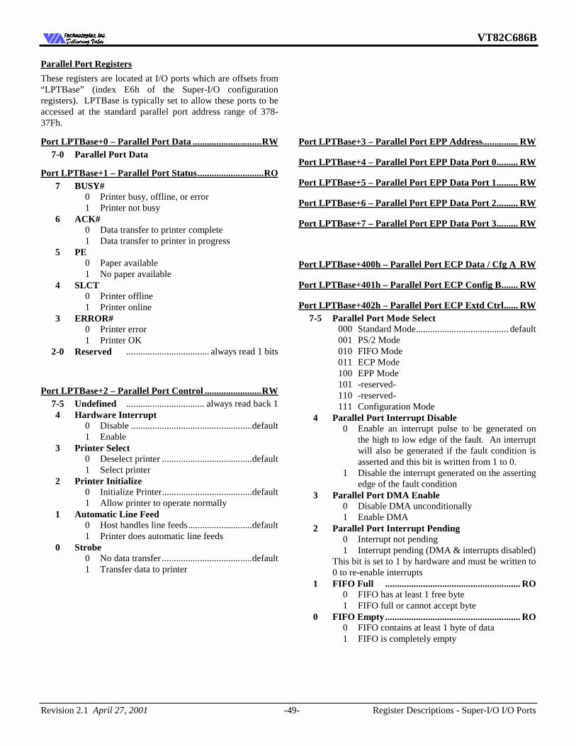
VT82C686B
Revision 2.1 April 27, 2001 -49- Register Descriptions - Super-I/O I/O Ports
7HFKQRORJLHV ,QF'HOLYHULQJ 9DOXH'HOLYHULQJ 9DOXH
Parallel Port Registers
These registers are located at I/O ports which are offsets from “LPTBase” (index E6h of the Super-I/O configuration registers). LPTBase is typically set to allow these ports to be accessed at the standard parallel port address range of 378-37Fh.
Port LPTBase+0 – Parallel Port Data .............................RW 7-0 Parallel Port Data
Port LPTBase+1 – Parallel Port Status............................RO 7 BUSY# 0 Printer busy, offline, or error 1 Printer not busy 6 ACK# 0 Data transfer to printer complete 1 Data transfer to printer in progress 5 PE 0 Paper available 1 No paper available 4 SLCT 0 Printer offline 1 Printer online 3 ERROR# 0 Printer error 1 Printer OK 2-0 Reserved ................................... always read 1 bits
Port LPTBase+2 – Parallel Port Control ........................RW 7-5 Undefined ................................. always read back 1 4 Hardware Interrupt 0 Disable ...................................................default 1 Enable 3 Printer Select 0 Deselect printer ......................................default 1 Select printer 2 Printer Initialize 0 Initialize Printer......................................default 1 Allow printer to operate normally 1 Automatic Line Feed 0 Host handles line feeds...........................default 1 Printer does automatic line feeds 0 Strobe 0 No data transfer ......................................default 1 Transfer data to printer
Port LPTBase+3 – Parallel Port EPP Address............... RW
Port LPTBase+4 – Parallel Port EPP Data Port 0......... RW
Port LPTBase+5 – Parallel Port EPP Data Port 1......... RW
Port LPTBase+6 – Parallel Port EPP Data Port 2......... RW
Port LPTBase+7 – Parallel Port EPP Data Port 3......... RW
Port LPTBase+400h – Parallel Port ECP Data / Cfg A RW
Port LPTBase+401h – Parallel Port ECP Config B....... RW
Port LPTBase+402h – Parallel Port ECP Extd Ctrl...... RW 7-5 Parallel Port Mode Select 000 Standard Mode....................................... default 001 PS/2 Mode 010 FIFO Mode 011 ECP Mode 100 EPP Mode 101 -reserved- 110 -reserved- 111 Configuration Mode 4 Parallel Port Interrupt Disable 0 Enable an interrupt pulse to be generated on
the high to low edge of the fault. An interrupt will also be generated if the fault condition is asserted and this bit is written from 1 to 0.
1 Disable the interrupt generated on the asserting edge of the fault condition
3 Parallel Port DMA Enable 0 Disable DMA unconditionally 1 Enable DMA 2 Parallel Port Interrupt Pending 0 Interrupt not pending 1 Interrupt pending (DMA & interrupts disabled) This bit is set to 1 by hardware and must be written to
0 to re-enable interrupts 1 FIFO Full ......................................................... RO 0 FIFO has at least 1 free byte 1 FIFO full or cannot accept byte 0 FIFO Empty......................................................... RO 0 FIFO contains at least 1 byte of data 1 FIFO is completely empty
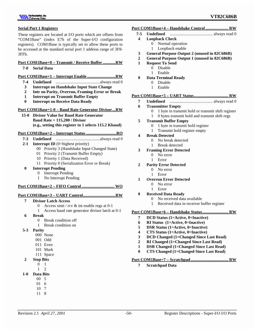
VT82C686B
Revision 2.1 April 27, 2001 -50- Register Descriptions - Super-I/O I/O Ports
7HFKQRORJLHV ,QF'HOLYHULQJ 9DOXH'HOLYHULQJ 9DOXH
Serial Port 1 Registers
These registers are located at I/O ports which are offsets from “COM1Base” (index E7h of the Super-I/O configuration registers). COM1Base is typically set to allow these ports to be accessed at the standard serial port 1 address range of 3F8-3FFh.
Port COM1Base+0 – Transmit / Receive Buffer ............RW 7-0 Serial Data
Port COM1Base+1 – Interrupt Enable ...........................RW 7-4 Undefined ..........................................always read 0 3 Interrupt on Handshake Input State Change 2 Intr on Parity, Overrun, Framing Error or Break 1 Interrupt on Transmit Buffer Empty 0 Interrupt on Receive Data Ready
Port COM1Base+1-0 – Baud Rate Generator Divisor...RW 15-0 Divisor Value for Baud Rate Generator Baud Rate = 115,200 / Divisor (e.g., setting this register to 1 selects 115.2 Kbaud)
Port COM1Base+2 – Interrupt Status .............................RO 7-3 Undefined ..........................................always read 0 2-1 Interrupt ID (0=highest priority) 00 Priority 3 (Handshake Input Changed State) 01 Priority 2 (Transmit Buffer Empty) 10 Priority 1 (Data Received) 11 Priority 0 (Serialization Error or Break) 0 Interrupt Pending 0 Interrupt Pending 1 No Interrupt Pending
Port COM1Base+2 – FIFO Control ............................... WO
Port COM1Base+3 – UART Control...............................RW 7 Divisor Latch Access 0 Access xmit / rcv & int enable regs at 0-1 1 Access baud rate generator divisor latch at 0-1 6 Break 0 Break condition off 1 Break condition on 5-3 Parity 000 None 001 Odd 011 Even 101 Mark 111 Space 2 Stop Bits 0 1 1 2 1-0 Data Bits 00 5 01 6 10 7 11 8
Port COM1Base+4 – Handshake Control ...................... RW 7-5 Undefined ......................................... always read 0 4 Loopback Check 0 Normal operation 1 Loopback enable 3 General Purpose Output 2 (unused in 82C686B) 2 General Purpose Output 1 (unused in 82C686B) 1 Request To Send 0 Disable 1 Enable 0 Data Terminal Ready 0 Disable 1 Enable
Port COM1Base+5 – UART Status................................. RW 7 Undefined ......................................... always read 0 6 Transmitter Empty 0 1 byte in transmit hold or transmit shift register 1 0 bytes transmit hold and transmit shift regs 5 Transmit Buffer Empty 0 1 byte in transmit hold register 1 Transmit hold register empty 4 Break Detected 0 No break detected 1 Break detected 3 Framing Error Detected 0 No error 1 Error 2 Parity Error Detected 0 No error 1 Error 1 Overrun Error Detected 0 No error 1 Error 0 Received Data Ready 0 No received data available 1 Received data in receiver buffer register
Port COM1Base+6 – Handshake Status......................... RW 7 DCD Status (1=Active, 0=Inactive) 6 RI Status (1=Active, 0=Inactive) 5 DSR Status (1=Active, 0=Inactive) 4 CTS Status (1=Active, 0=Inactive) 3 DCD Changed (1=Changed Since Last Read) 2 RI Changed (1=Changed Since Last Read) 1 DSR Changed (1=Changed Since Last Read) 0 CTS Changed (1=Changed Since Last Read)
Port COM1Base+7 – Scratchpad .................................... RW 7 Scratchpad Data
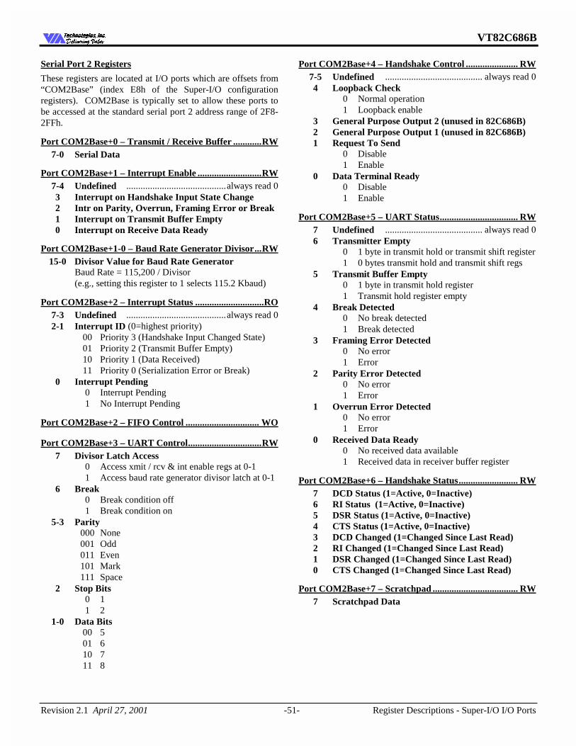
VT82C686B
Revision 2.1 April 27, 2001 -51- Register Descriptions - Super-I/O I/O Ports
7HFKQRORJLHV ,QF'HOLYHULQJ 9DOXH'HOLYHULQJ 9DOXH
Serial Port 2 Registers
These registers are located at I/O ports which are offsets from “COM2Base” (index E8h of the Super-I/O configuration registers). COM2Base is typically set to allow these ports to be accessed at the standard serial port 2 address range of 2F8-2FFh.
Port COM2Base+0 – Transmit / Receive Buffer ............RW 7-0 Serial Data
Port COM2Base+1 – Interrupt Enable ...........................RW 7-4 Undefined ..........................................always read 0 3 Interrupt on Handshake Input State Change 2 Intr on Parity, Overrun, Framing Error or Break 1 Interrupt on Transmit Buffer Empty 0 Interrupt on Receive Data Ready
Port COM2Base+1-0 – Baud Rate Generator Divisor...RW 15-0 Divisor Value for Baud Rate Generator Baud Rate = 115,200 / Divisor (e.g., setting this register to 1 selects 115.2 Kbaud)
Port COM2Base+2 – Interrupt Status .............................RO 7-3 Undefined ..........................................always read 0 2-1 Interrupt ID (0=highest priority) 00 Priority 3 (Handshake Input Changed State) 01 Priority 2 (Transmit Buffer Empty) 10 Priority 1 (Data Received) 11 Priority 0 (Serialization Error or Break) 0 Interrupt Pending 0 Interrupt Pending 1 No Interrupt Pending
Port COM2Base+2 – FIFO Control ............................... WO
Port COM2Base+3 – UART Control...............................RW 7 Divisor Latch Access 0 Access xmit / rcv & int enable regs at 0-1 1 Access baud rate generator divisor latch at 0-1 6 Break 0 Break condition off 1 Break condition on 5-3 Parity 000 None 001 Odd 011 Even 101 Mark 111 Space 2 Stop Bits 0 1 1 2 1-0 Data Bits 00 5 01 6 10 7 11 8
Port COM2Base+4 – Handshake Control ...................... RW 7-5 Undefined ......................................... always read 0 4 Loopback Check 0 Normal operation 1 Loopback enable 3 General Purpose Output 2 (unused in 82C686B) 2 General Purpose Output 1 (unused in 82C686B) 1 Request To Send 0 Disable 1 Enable 0 Data Terminal Ready 0 Disable 1 Enable
Port COM2Base+5 – UART Status................................. RW 7 Undefined ......................................... always read 0 6 Transmitter Empty 0 1 byte in transmit hold or transmit shift register 1 0 bytes transmit hold and transmit shift regs 5 Transmit Buffer Empty 0 1 byte in transmit hold register 1 Transmit hold register empty 4 Break Detected 0 No break detected 1 Break detected 3 Framing Error Detected 0 No error 1 Error 2 Parity Error Detected 0 No error 1 Error 1 Overrun Error Detected 0 No error 1 Error 0 Received Data Ready 0 No received data available 1 Received data in receiver buffer register
Port COM2Base+6 – Handshake Status......................... RW 7 DCD Status (1=Active, 0=Inactive) 6 RI Status (1=Active, 0=Inactive) 5 DSR Status (1=Active, 0=Inactive) 4 CTS Status (1=Active, 0=Inactive) 3 DCD Changed (1=Changed Since Last Read) 2 RI Changed (1=Changed Since Last Read) 1 DSR Changed (1=Changed Since Last Read) 0 CTS Changed (1=Changed Since Last Read)
Port COM2Base+7 – Scratchpad .................................... RW 7 Scratchpad Data
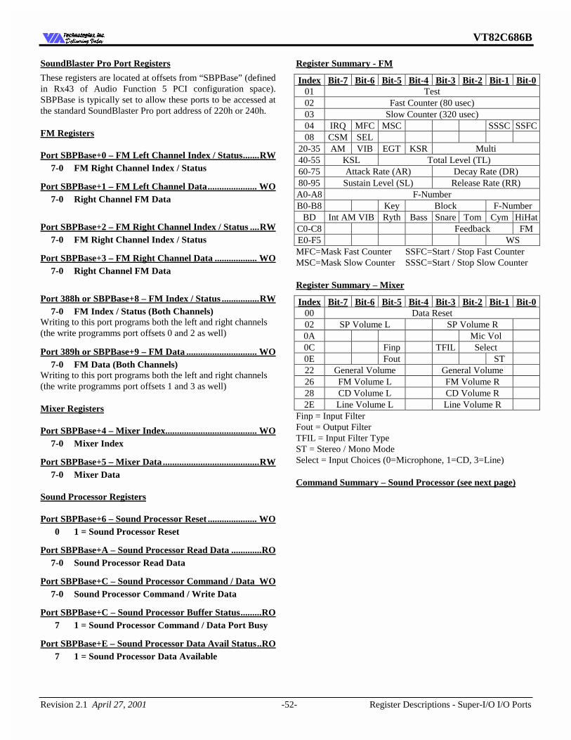
VT82C686B
Revision 2.1 April 27, 2001 -52- Register Descriptions - Super-I/O I/O Ports
7HFKQRORJLHV ,QF'HOLYHULQJ 9DOXH'HOLYHULQJ 9DOXH
SoundBlaster Pro Port Registers
These registers are located at offsets from “SBPBase” (defined in Rx43 of Audio Function 5 PCI configuration space). SBPBase is typically set to allow these ports to be accessed at the standard SoundBlaster Pro port address of 220h or 240h.
FM Registers
Port SBPBase+0 – FM Left Channel Index / Status.......RW 7-0 FM Right Channel Index / Status
Port SBPBase+1 – FM Left Channel Data..................... WO 7-0 Right Channel FM Data
Port SBPBase+2 – FM Right Channel Index / Status ....RW 7-0 FM Right Channel Index / Status
Port SBPBase+3 – FM Right Channel Data .................. WO 7-0 Right Channel FM Data
Port 388h or SBPBase+8 – FM Index / Status ................RW 7-0 FM Index / Status (Both Channels) Writing to this port programs both the left and right channels (the write programms port offsets 0 and 2 as well)
Port 389h or SBPBase+9 – FM Data .............................. WO 7-0 FM Data (Both Channels) Writing to this port programs both the left and right channels (the write programms port offsets 1 and 3 as well)
Mixer Registers
Port SBPBase+4 – Mixer Index....................................... WO 7-0 Mixer Index
Port SBPBase+5 – Mixer Data .........................................RW 7-0 Mixer Data
Sound Processor Registers
Port SBPBase+6 – Sound Processor Reset ..................... WO 0 1 = Sound Processor Reset
Port SBPBase+A – Sound Processor Read Data .............RO 7-0 Sound Processor Read Data
Port SBPBase+C – Sound Processor Command / Data WO 7-0 Sound Processor Command / Write Data
Port SBPBase+C – Sound Processor Buffer Status.........RO 7 1 = Sound Processor Command / Data Port Busy
Port SBPBase+E – Sound Processor Data Avail Status..RO 7 1 = Sound Processor Data Available
Register Summary - FM
Index Bit-7 Bit-6 Bit-5 Bit-4 Bit-3 Bit-2 Bit-1 Bit-0 01 Test 02 Fast Counter (80 usec) 03 Slow Counter (320 usec) 04 IRQ MFC MSC SSSC SSFC 08 CSM SEL
20-35 AM VIB EGT KSR Multi 40-55 KSL Total Level (TL) 60-75 Attack Rate (AR) Decay Rate (DR) 80-95 Sustain Level (SL) Release Rate (RR) A0-A8 F-Number B0-B8 Key Block F-Number
BD Int AM VIB Ryth Bass Snare Tom Cym HiHat C0-C8 Feedback FM E0-F5 WS MFC=Mask Fast Counter SSFC=Start / Stop Fast Counter MSC=Mask Slow Counter SSSC=Start / Stop Slow Counter
Register Summary – Mixer
Index Bit-7 Bit-6 Bit-5 Bit-4 Bit-3 Bit-2 Bit-1 Bit-0 00 Data Reset 02 SP Volume L SP Volume R 0A Mic Vol 0C Finp TFIL Select 0E Fout ST 22 General Volume General Volume 26 FM Volume L FM Volume R 28 CD Volume L CD Volume R 2E Line Volume L Line Volume R
Finp = Input Filter Fout = Output Filter TFIL = Input Filter Type ST = Stereo / Mono Mode Select = Input Choices (0=Microphone, 1=CD, 3=Line)
Command Summary – Sound Processor (see next page)
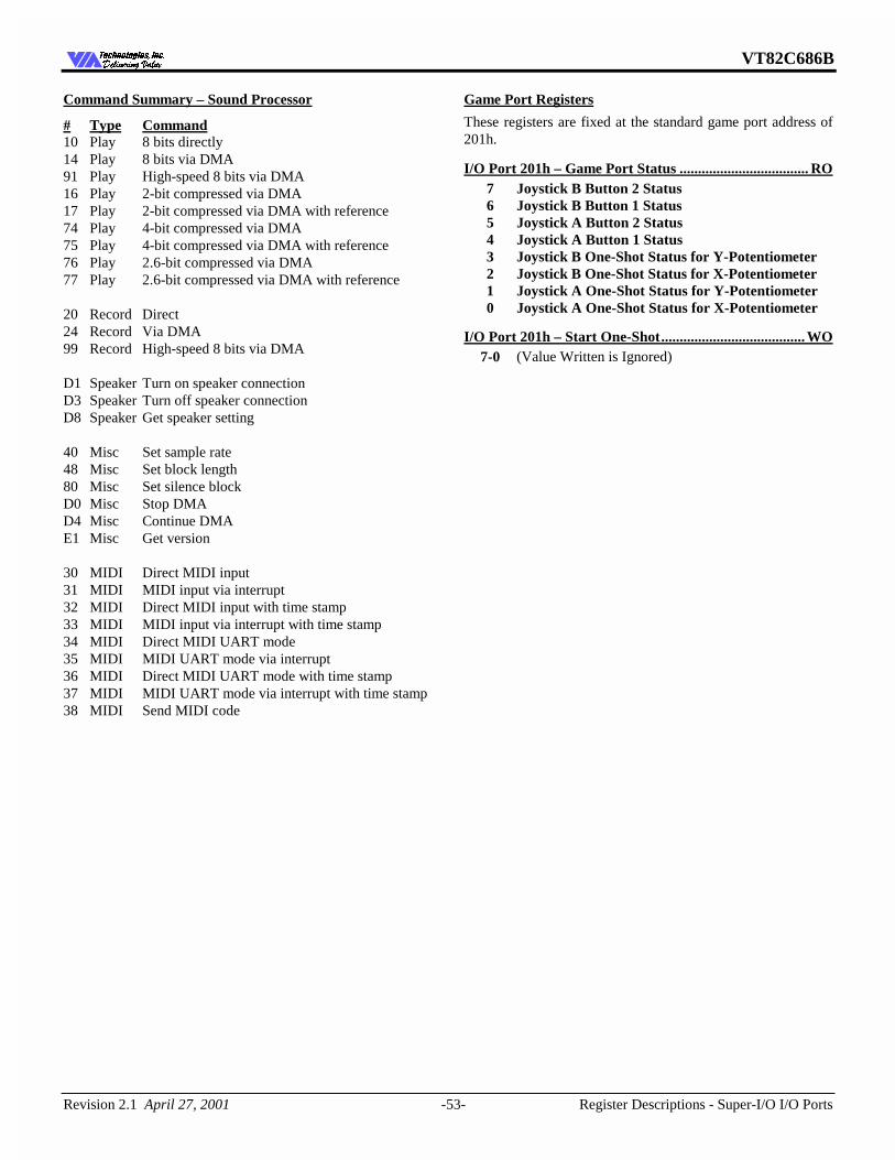
VT82C686B
Revision 2.1 April 27, 2001 -53- Register Descriptions - Super-I/O I/O Ports
7HFKQRORJLHV ,QF'HOLYHULQJ 9DOXH'HOLYHULQJ 9DOXH
Command Summary – Sound Processor
# Type Command 10 Play 8 bits directly 14 Play 8 bits via DMA 91 Play High-speed 8 bits via DMA 16 Play 2-bit compressed via DMA 17 Play 2-bit compressed via DMA with reference 74 Play 4-bit compressed via DMA 75 Play 4-bit compressed via DMA with reference 76 Play 2.6-bit compressed via DMA 77 Play 2.6-bit compressed via DMA with reference 20 Record Direct 24 Record Via DMA 99 Record High-speed 8 bits via DMA D1 Speaker Turn on speaker connection D3 Speaker Turn off speaker connection D8 Speaker Get speaker setting 40 Misc Set sample rate 48 Misc Set block length 80 Misc Set silence block D0 Misc Stop DMA D4 Misc Continue DMA E1 Misc Get version 30 MIDI Direct MIDI input 31 MIDI MIDI input via interrupt 32 MIDI Direct MIDI input with time stamp 33 MIDI MIDI input via interrupt with time stamp 34 MIDI Direct MIDI UART mode 35 MIDI MIDI UART mode via interrupt 36 MIDI Direct MIDI UART mode with time stamp 37 MIDI MIDI UART mode via interrupt with time stamp 38 MIDI Send MIDI code
Game Port Registers
These registers are fixed at the standard game port address of 201h.
I/O Port 201h – Game Port Status ................................... RO 7 Joystick B Button 2 Status 6 Joystick B Button 1 Status 5 Joystick A Button 2 Status 4 Joystick A Button 1 Status 3 Joystick B One-Shot Status for Y-Potentiometer 2 Joystick B One-Shot Status for X-Potentiometer 1 Joystick A One-Shot Status for Y-Potentiometer 0 Joystick A One-Shot Status for X-Potentiometer
I/O Port 201h – Start One-Shot....................................... WO 7-0 (Value Written is Ignored)
VT82C686B
Revision 2.1 April 27, 2001 -54- Function 0 Registers - PCI to ISA Bridge
7HFKQRORJLHV ,QF'HOLYHULQJ 9DOXH'HOLYHULQJ 9DOXH
PCI Configuration Space I/O
PCI configuration space accesses for functions 0-6 use PCI configuration mechanism 1 (see PCI specification revision 2.2 for more details). The ports respond only to double-word accesses. Byte or word accesses will be passed on unchanged.
Port CFB-CF8 - Configuration Address .........................RW 31 Configuration Space Enable 0 Disable ...................................................default 1 Convert configuration data port writes to
configuration cycles on the PCI bus 30-24 Reserved ........................................ always reads 0 23-16 PCI Bus Number Used to choose a specific PCI bus in the system 15-11 Device Number Used to choose a specific device in the system 10-8 Function Number Used to choose a specific function if the selected
device supports multiple functions 7-2 Register Number Used to select a specific DWORD in the device’s
configuration space 1-0 Fixed ........................................ always reads 0
Port CFF-CFC - Configuration Data ..............................RW
There are 7 “functions” implemented in the VT82C686B:
Function # Function
0 PCI to ISA Bridge
1 IDE Controller
2 USB Controller Ports 0-1
3 USB Controller Ports 2-3
4 Power Management, SMBus & Hardware Monitor
5 AC97 Audio Codec Controller
6 MC97 Modem Codec Controller
The following sections describe the registers and register bits of these functions.
VT82C686B
Revision 2.1 April 27, 2001 -55- Function 0 Registers - PCI to ISA Bridge
7HFKQRORJLHV ,QF'HOLYHULQJ 9DOXH'HOLYHULQJ 9DOXH
Function 0 Registers - PCI to ISA Bridge
All registers are located in the function 0 PCI configuration space of the VT82C686B. These registers are accessed through PCI configuration mechanism #1 via I/O address CF8/CFC.
PCI Configuration Space Header
Offset 1-0 - Vendor ID = 1106h.........................................RO
Offset 3-2 - Device ID = 0686h ..........................................RO
Offset 5-4 - Command.......................................................RW 15-8 Reserved ........................................ always reads 0 7 Address / Data Stepping 0 Disable 1 Enable ....................................................default 6-4 Reserved ........................................ always reads 0 3 Special Cycle Enable .....Normally RW†, default = 0 2 Bus Master ........................................ always reads 1 1 Memory Space.................. Normally RO†, reads as 1 0 I/O Space ...................... Normally RO†, reads as 1 † If the Rx46[4] test bit is set, access to bits 0, 1, and 3 above is reversed: bit-3 becomes read only (reading back 1) and bits 0-1 become read / write (with a default of 1).
Offset 7-6 - Status...........................................................RWC 15 Detected Parity Error ....................write one to clear 14 Signalled System Error...................... always reads 0 13 Signalled Master Abort .................write one to clear 12 Received Target Abort ..................write one to clear 11 Signalled Target Abort ..................write one to clear 10-9 DEVSEL# Timing .................... fixed at 01 (medium) 8 Data Parity Detected.......................... always reads 0 7 Fast Back-to-Back.............................. always reads 0 6-0 Reserved ........................................ always reads 0
Offset 8 - Revision ID = nn ................................................RO 7-0 Revision ID 0x VT82C686 1x VT82C686A 4x VT82C686B
Offset 9 - Program Interface = 00h...................................RO
Offset A - Sub Class Code = 01h .......................................RO
Offset B - Class Code = 06h...............................................RO
Offset E - Header Type = 80h............................................RO 7-0 Header Type Code .........80h (Multifunction Device)
Offset F - BIST = 00h.........................................................RO
Offset 2F-2C - Subsystem ID.............................................RO Use offset 70-73 to change the value returned.
Offset 34 – Power Management Capability Ptr = C0h ...RO
ISA Bus Control
Offset 40 - ISA Bus Control ............................................. RW 7 ISA Command Delay 0 Normal................................................... default 1 Extra 6 Extended ISA Bus Ready 0 Disable................................................... default 1 Enable 5 ISA Slave Wait States 0 4 Wait States.......................................... default 1 5 Wait States 4 Chipset I/O Wait States 0 2 Wait States.......................................... default 1 4 Wait States 3 I/O Recovery Time 0 Disable................................................... default 1 Enable 2 Extend-ALE 0 Disable................................................... default 1 Enable 1 ROM Wait States 0 1 Wait State ........................................... default 1 0 Wait States 0 ROM Write 0 Disable................................................... default 1 Enable
Offset 41 - ISA Test Mode................................................ RW 7 Bus Refresh Arbitration (do not program) default=0 6 I/O Recovery Time 0 Normal (13 BCLKs) .............................. default 1 Medium (8 BCLKs) 5 Port 92 Fast Reset 0 Disable................................................... default 1 Enable 4 A20G Emulation (do not program) .............default=0 3 Double DMA Clock 0 Disable (DMA Clock = ½ ISA Clock)... default 1 Enable (DMA Clock = ISA Clock) This function can be enabled for external ISA devices
(e.g., advanced Super-IO or FIR controllers) which support 8MHz DMA channels. However, if this bit is set to 1, then all DMA channels will be 8 MHz. If this bit is set to 1 and Rx45[n] is set to 1, then ISA DMA channel ‘n’ will be 16 MHz. Therefore, typically this bit is set to 0 and the appropriate bits of Rx45 should be set to 1 to enable 8 MHz DMA clock only for specific channels that support the higher rate.
2 SHOLD Lock During INTA (do not program) def=0 1 Refresh Request Test Mode (do not program).def=0 0 ISA Refresh 0 Disable................................................... default 1 Enable This bit should be set to 1 for ISA compatibility.
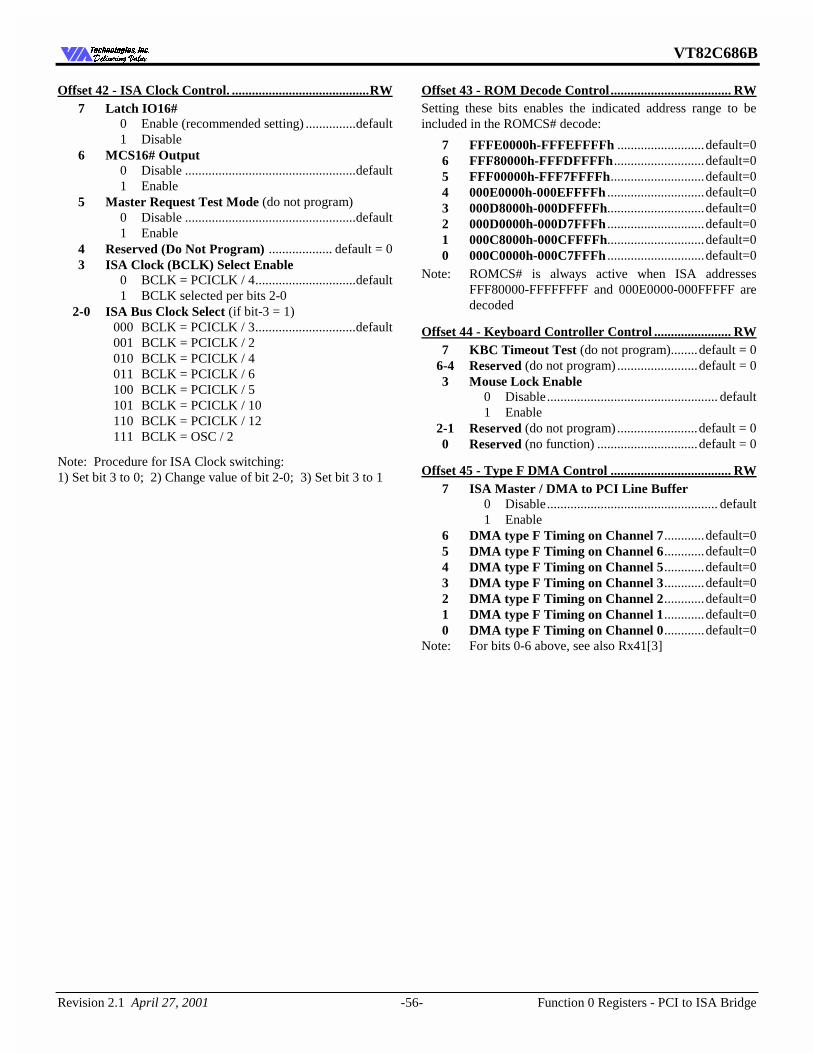
VT82C686B
Revision 2.1 April 27, 2001 -56- Function 0 Registers - PCI to ISA Bridge
7HFKQRORJLHV ,QF'HOLYHULQJ 9DOXH'HOLYHULQJ 9DOXH
Offset 42 - ISA Clock Control. .........................................RW 7 Latch IO16# 0 Enable (recommended setting) ...............default 1 Disable 6 MCS16# Output 0 Disable ...................................................default 1 Enable 5 Master Request Test Mode (do not program) 0 Disable ...................................................default 1 Enable 4 Reserved (Do Not Program) ................... default = 0 3 ISA Clock (BCLK) Select Enable 0 BCLK = PCICLK / 4..............................default 1 BCLK selected per bits 2-0 2-0 ISA Bus Clock Select (if bit-3 = 1) 000 BCLK = PCICLK / 3..............................default 001 BCLK = PCICLK / 2 010 BCLK = PCICLK / 4 011 BCLK = PCICLK / 6 100 BCLK = PCICLK / 5 101 BCLK = PCICLK / 10 110 BCLK = PCICLK / 12 111 BCLK = OSC / 2
Note: Procedure for ISA Clock switching: 1) Set bit 3 to 0; 2) Change value of bit 2-0; 3) Set bit 3 to 1
Offset 43 - ROM Decode Control .................................... RW Setting these bits enables the indicated address range to be included in the ROMCS# decode:
7 FFFE0000h-FFFEFFFFh ..........................default=0 6 FFF80000h-FFFDFFFFh...........................default=0 5 FFF00000h-FFF7FFFFh............................default=0 4 000E0000h-000EFFFFh .............................default=0 3 000D8000h-000DFFFFh.............................default=0 2 000D0000h-000D7FFFh .............................default=0 1 000C8000h-000CFFFFh.............................default=0 0 000C0000h-000C7FFFh .............................default=0 Note: ROMCS# is always active when ISA addresses
FFF80000-FFFFFFFF and 000E0000-000FFFFF are decoded
Offset 44 - Keyboard Controller Control ....................... RW 7 KBC Timeout Test (do not program)........default = 0 6-4 Reserved (do not program) ........................default = 0 3 Mouse Lock Enable 0 Disable................................................... default 1 Enable 2-1 Reserved (do not program) ........................default = 0 0 Reserved (no function) ..............................default = 0
Offset 45 - Type F DMA Control .................................... RW 7 ISA Master / DMA to PCI Line Buffer 0 Disable................................................... default 1 Enable 6 DMA type F Timing on Channel 7............default=0 5 DMA type F Timing on Channel 6............default=0 4 DMA type F Timing on Channel 5............default=0 3 DMA type F Timing on Channel 3............default=0 2 DMA type F Timing on Channel 2............default=0 1 DMA type F Timing on Channel 1............default=0 0 DMA type F Timing on Channel 0............default=0 Note: For bits 0-6 above, see also Rx41[3]
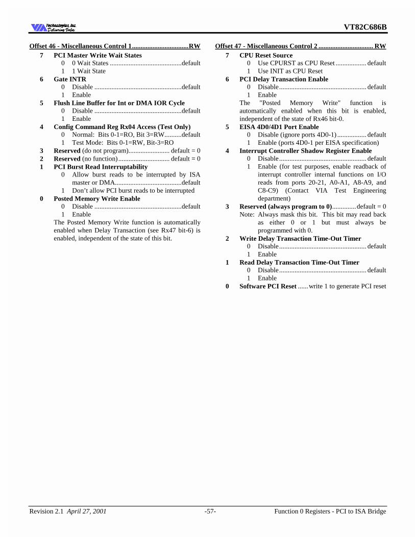
VT82C686B
Revision 2.1 April 27, 2001 -57- Function 0 Registers - PCI to ISA Bridge
7HFKQRORJLHV ,QF'HOLYHULQJ 9DOXH'HOLYHULQJ 9DOXH
Offset 46 - Miscellaneous Control 1.................................RW 7 PCI Master Write Wait States 0 0 Wait States ..........................................default 1 1 Wait State 6 Gate INTR 0 Disable ...................................................default 1 Enable 5 Flush Line Buffer for Int or DMA IOR Cycle 0 Disable ...................................................default 1 Enable 4 Config Command Reg Rx04 Access (Test Only) 0 Normal: Bits 0-1=RO, Bit 3=RW..........default 1 Test Mode: Bits 0-1=RW, Bit-3=RO 3 Reserved (do not program)........................ default = 0 2 Reserved (no function) .............................. default = 0 1 PCI Burst Read Interruptability 0 Allow burst reads to be interrupted by ISA
master or DMA.......................................default 1 Don’t allow PCI burst reads to be interrupted 0 Posted Memory Write Enable 0 Disable ...................................................default 1 Enable The Posted Memory Write function is automatically
enabled when Delay Transaction (see Rx47 bit-6) is enabled, independent of the state of this bit.
Offset 47 - Miscellaneous Control 2 ................................ RW 7 CPU Reset Source 0 Use CPURST as CPU Reset .................. default 1 Use INIT as CPU Reset 6 PCI Delay Transaction Enable 0 Disable................................................... default 1 Enable The "Posted Memory Write" function is
automatically enabled when this bit is enabled, independent of the state of Rx46 bit-0.
5 EISA 4D0/4D1 Port Enable 0 Disable (ignore ports 4D0-1) ................. default 1 Enable (ports 4D0-1 per EISA specification) 4 Interrupt Controller Shadow Register Enable 0 Disable................................................... default 1 Enable (for test purposes, enable readback of
interrupt controller internal functions on I/O reads from ports 20-21, A0-A1, A8-A9, and C8-C9) (Contact VIA Test Engineering department)
3 Reserved (always program to 0)..............default = 0 Note: Always mask this bit. This bit may read back
as either 0 or 1 but must always be programmed with 0.
2 Write Delay Transaction Time-Out Timer 0 Disable................................................... default 1 Enable 1 Read Delay Transaction Time-Out Timer 0 Disable................................................... default 1 Enable 0 Software PCI Reset ......write 1 to generate PCI reset
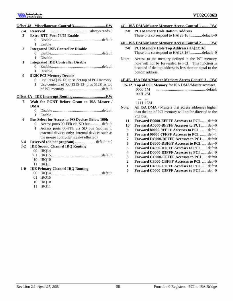
VT82C686B
Revision 2.1 April 27, 2001 -58- Function 0 Registers - PCI to ISA Bridge
7HFKQRORJLHV ,QF'HOLYHULQJ 9DOXH'HOLYHULQJ 9DOXH
Offset 48 - Miscellaneous Control 3.................................RW 7-4 Reserved ........................................ always reads 0 3 Extra RTC Port 74/75 Enable 0 Disable ...................................................default 1 Enable 2 Integrated USB Controller Disable 0 Enable.....................................................default 1 Disable 1 Integrated IDE Controller Disable 0 Enable.....................................................default 1 Disable 0 512K PCI Memory Decode 0 Use Rx4E[15-12] to select top of PCI memory 1 Use contents of Rx4E[15-12] plus 512K as top
of PCI memory .......................................default
Offset 4A - IDE Interrupt Routing ..................................RW 7 Wait for PGNT Before Grant to ISA Master /
DMA 0 Disable ...................................................default 1 Enable 6 Bus Select for Access to I/O Devices Below 100h 0 Access ports 00-FFh via XD bus............default 1 Access ports 00-FFh via SD bus (applies to
external devices only; internal devices such as the mouse controller are not effected)
5-4 Reserved (do not program) ..................... default = 0 3-2 IDE Second Channel IRQ Routing 00 IRQ14 01 IRQ15.....................................................default 10 IRQ10 11 IRQ11 1-0 IDE Primary Channel IRQ Routing 00 IRQ14.....................................................default 01 IRQ15 10 IRQ10 11 IRQ11
4C - ISA DMA/Master Memory Access Control 1 ........ RW 7-0 PCI Memory Hole Bottom Address These bits correspond to HA[23:16] ............default=0
4D - ISA DMA/Master Memory Access Control 2 ........ RW 7-0 PCI Memory Hole Top Address (HA[23:16]) These bits correspond to HA[23:16] ............default=0
Note: Access to the memory defined in the PCI memory hole will not be forwarded to PCI. This function is disabled if the top address is less than or equal to the bottom address.
4F-4E - ISA DMA/Master Memory Access Control 3 ... RW 15-12 Top of PCI Memory for ISA DMA/Master accesses 0000 1M .................................................... default 0001 2M ... ... 1111 16M Note: All ISA DMA / Masters that access addresses higher
than the top of PCI memory will not be directed to the PCI bus.
11 Forward E0000-EFFFF Accesses to PCI........def=0 10 Forward A0000-BFFFF Accesses to PCI .......def=0 9 Forward 80000-9FFFF Accesses to PCI ........def=1 8 Forward 00000-7FFFF Accesses to PCI ........def=1 7 Forward DC000-DFFFF Accesses to PCI ......def=0 6 Forward D8000-DBFFF Accesses to PCI ......def=0 5 Forward D4000-D7FFF Accesses to PCI .......def=0 4 Forward D0000-D3FFF Accesses to PCI .......def=0 3 Forward CC000-CFFFF Accesses to PCI .....def=0 2 Forward C8000-CBFFF Accesses to PCI ......def=0 1 Forward C4000-C7FFF Accesses to PCI .......def=0 0 Forward C0000-C3FFF Accesses to PCI .......def=0
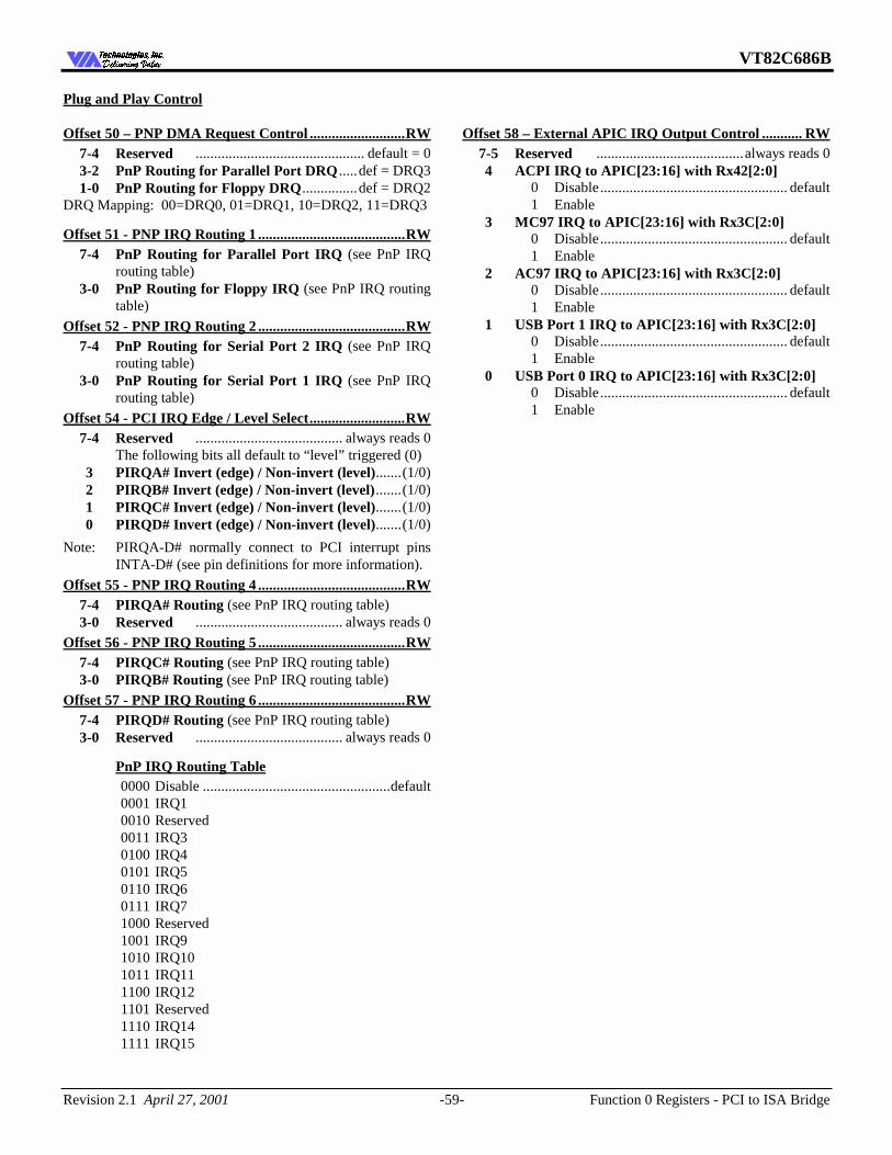
VT82C686B
Revision 2.1 April 27, 2001 -59- Function 0 Registers - PCI to ISA Bridge
7HFKQRORJLHV ,QF'HOLYHULQJ 9DOXH'HOLYHULQJ 9DOXH
Plug and Play Control
Offset 50 – PNP DMA Request Control ..........................RW 7-4 Reserved .............................................. default = 0 3-2 PnP Routing for Parallel Port DRQ .....def = DRQ3 1-0 PnP Routing for Floppy DRQ...............def = DRQ2 DRQ Mapping: 00=DRQ0, 01=DRQ1, 10=DRQ2, 11=DRQ3
Offset 51 - PNP IRQ Routing 1 ........................................RW 7-4 PnP Routing for Parallel Port IRQ (see PnP IRQ
routing table) 3-0 PnP Routing for Floppy IRQ (see PnP IRQ routing
table)
Offset 52 - PNP IRQ Routing 2 ........................................RW 7-4 PnP Routing for Serial Port 2 IRQ (see PnP IRQ
routing table) 3-0 PnP Routing for Serial Port 1 IRQ (see PnP IRQ
routing table)
Offset 54 - PCI IRQ Edge / Level Select..........................RW 7-4 Reserved ........................................ always reads 0 The following bits all default to “level” triggered (0) 3 PIRQA# Invert (edge) / Non-invert (level).......(1/0) 2 PIRQB# Invert (edge) / Non-invert (level).......(1/0) 1 PIRQC# Invert (edge) / Non-invert (level).......(1/0) 0 PIRQD# Invert (edge) / Non-invert (level).......(1/0)
Note: PIRQA-D# normally connect to PCI interrupt pins INTA-D# (see pin definitions for more information).
Offset 55 - PNP IRQ Routing 4 ........................................RW 7-4 PIRQA# Routing (see PnP IRQ routing table) 3-0 Reserved ........................................ always reads 0
Offset 56 - PNP IRQ Routing 5 ........................................RW 7-4 PIRQC# Routing (see PnP IRQ routing table) 3-0 PIRQB# Routing (see PnP IRQ routing table)
Offset 57 - PNP IRQ Routing 6 ........................................RW 7-4 PIRQD# Routing (see PnP IRQ routing table) 3-0 Reserved ........................................ always reads 0
PnP IRQ Routing Table 0000 Disable ...................................................default 0001 IRQ1 0010 Reserved 0011 IRQ3 0100 IRQ4 0101 IRQ5 0110 IRQ6 0111 IRQ7 1000 Reserved 1001 IRQ9 1010 IRQ10 1011 IRQ11 1100 IRQ12 1101 Reserved 1110 IRQ14 1111 IRQ15
Offset 58 – External APIC IRQ Output Control ........... RW 7-5 Reserved ........................................always reads 0 4 ACPI IRQ to APIC[23:16] with Rx42[2:0] 0 Disable................................................... default 1 Enable 3 MC97 IRQ to APIC[23:16] with Rx3C[2:0] 0 Disable................................................... default 1 Enable 2 AC97 IRQ to APIC[23:16] with Rx3C[2:0] 0 Disable................................................... default 1 Enable 1 USB Port 1 IRQ to APIC[23:16] with Rx3C[2:0] 0 Disable................................................... default 1 Enable 0 USB Port 0 IRQ to APIC[23:16] with Rx3C[2:0] 0 Disable................................................... default 1 Enable
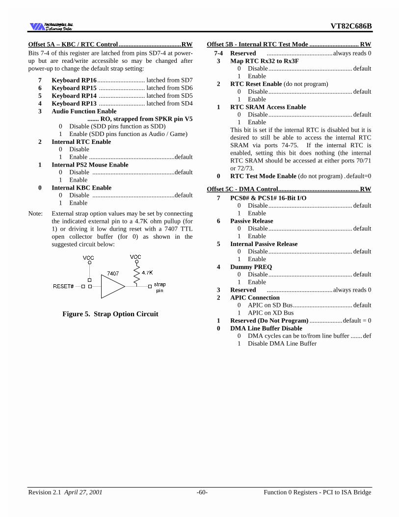
VT82C686B
Revision 2.1 April 27, 2001 -60- Function 0 Registers - PCI to ISA Bridge
7HFKQRORJLHV ,QF'HOLYHULQJ 9DOXH'HOLYHULQJ 9DOXH
Offset 5A – KBC / RTC Control ......................................RW Bits 7-4 of this register are latched from pins SD7-4 at power-up but are read/write accessible so may be changed after power-up to change the default strap setting:
7 Keyboard RP16 ............................. latched from SD7 6 Keyboard RP15 ............................ latched from SD6 5 Keyboard RP14 ............................ latched from SD5 4 Keyboard RP13 ............................ latched from SD4 3 Audio Function Enable ....... RO, strapped from SPKR pin V5 0 Disable (SDD pins function as SDD) 1 Enable (SDD pins function as Audio / Game) 2 Internal RTC Enable 0 Disable 1 Enable ....................................................default 1 Internal PS2 Mouse Enable 0 Disable ..................................................default 1 Enable 0 Internal KBC Enable 0 Disable ..................................................default 1 Enable
Note: External strap option values may be set by connecting the indicated external pin to a 4.7K ohm pullup (for 1) or driving it low during reset with a 7407 TTL open collector buffer (for 0) as shown in the suggested circuit below:
9&&
.
VWUDS
SLQ5(6(7
9&&
Figure 5. Strap Option Circuit
Offset 5B - Internal RTC Test Mode .............................. RW 7-4 Reserved ........................................always reads 0 3 Map RTC Rx32 to Rx3F 0 Disable................................................... default 1 Enable 2 RTC Reset Enable (do not program) 0 Disable................................................... default 1 Enable 1 RTC SRAM Access Enable 0 Disable................................................... default 1 Enable This bit is set if the internal RTC is disabled but it is
desired to still be able to access the internal RTC SRAM via ports 74-75. If the internal RTC is enabled, setting this bit does nothing (the internal RTC SRAM should be accessed at either ports 70/71 or 72/73.
0 RTC Test Mode Enable (do not program) .default=0
Offset 5C - DMA Control................................................. RW 7 PCS0# & PCS1# 16-Bit I/O 0 Disable................................................... default 1 Enable 6 Passive Release 0 Disable................................................... default 1 Enable 5 Internal Passive Release 0 Disable................................................... default 1 Enable 4 Dummy PREQ 0 Disable................................................... default 1 Enable 3 Reserved ........................................always reads 0 2 APIC Connection 0 APIC on SD Bus.................................... default 1 APIC on XD Bus 1 Reserved (Do Not Program) ....................default = 0 0 DMA Line Buffer Disable 0 DMA cycles can be to/from line buffer ....... def 1 Disable DMA Line Buffer
VT82C686B
Revision 2.1 April 27, 2001 -61- Function 0 Registers - PCI to ISA Bridge
7HFKQRORJLHV ,QF'HOLYHULQJ 9DOXH'HOLYHULQJ 9DOXH
Distributed DMA / Serial IRQ Control
Offset 61-60 - Distributed DMA Ch 0 Base / Enable......RW 15-4 Channel 0 Base Address Bits 15-4 .......... default = 0 3 Channel 0 Enable 0 Disable ...................................................default 1 Enable 2-0 Reserved ........................................ always reads 0
Offset 63-62 - Distributed DMA Ch 1 Base / Enable......RW 15-4 Channel 1 Base Address Bits 15-4 .......... default = 0 3 Channel 1 Enable 0 Disable ...................................................default 1 Enable 2-0 Reserved ........................................ always reads 0
Offset 65-64 - Distributed DMA Ch 2 Base / Enable......RW 15-4 Channel 2 Base Address Bits 15-4 .......... default = 0 3 Channel 2 Enable 0 Disable ...................................................default 1 Enable 2-0 Reserved ........................................ always reads 0
Offset 67-66 - Distributed DMA Ch 3 Base / Enable......RW 15-4 Channel 3 Base Address Bits 15-4 .......... default = 0 3 Channel 3 Enable 0 Disable ...................................................default 1 Enable 2-0 Reserved ........................................ always reads 0
Offset 69-68 – Serial IRQ Control ...................................RW 15-4 Reserved ........................................ always reads 0 3 ISA IRQ Asserted Via Serial IRQ (Pin H3 or L4) 0 Disable ...................................................default 1 Enable 2 Serial IRQ Mode 0 Continuous Mode ...................................default 1 Quiet Mode 1-0 Serial IRQ Start-Frame Width 00 4 PCI Clocks ..........................................default 01 6 PCI Clocks 10 8 PCI Clocks 11 10 PCI Clocks The frame size is fixed at 21 PCI clocks.
Offset 6B-6A - Distributed DMA Ch 5 Base / Enable.... RW 15-4 Channel 5 Base Address Bits 15-4...........default = 0 3 Channel 5 Enable 0 Disable................................................... default 1 Enable 2-0 Reserved ........................................always reads 0
Offset 6D-6C - Distributed DMA Ch 6 Base / Enable ... RW 15-4 Channel 6 Base Address Bits 15-4...........default = 0 3 Channel 6 Enable 0 Disable................................................... default 1 Enable 2-0 Reserved ........................................always reads 0
Offset 6F-6E - Distributed DMA Ch 7 Base / Enable .... RW 15-4 Channel 7 Base Address Bits 15-4...........default = 0 3 Channel 7 Enable 0 Disable................................................... default 1 Enable 2-0 Reserved ........................................always reads 0
VT82C686B
Revision 2.1 April 27, 2001 -62- Function 0 Registers - PCI to ISA Bridge
7HFKQRORJLHV ,QF'HOLYHULQJ 9DOXH'HOLYHULQJ 9DOXH
Miscellaneous / General Purpose I/O
Offset 73-70 - Subsystem ID ............................................ WO 31-0 Subsystem ID / Vendor ID................. always reads 0 Contents may be read at offset 2C.
Offset 74 – GPIO Control 1..............................................RW 7 Reserved (Do Not Program).................... default = 0 6 SERIRQ Pin 0 SERIRQ input from DRQ2 (Pin H3)......default 1 SERIRQ input from DACK5# (Pin L4) 5 GPIOD Direction (Pin U8) 0 Input .....................................................default 1 Output (GPO11) 4 GPIOC Direction (Pin V14) 0 Input .....................................................default 1 Output 3 GPIOB Direction (Pin U12) 0 Input .....................................................default 1 Output 2 GPIOA Direction (Pin T14) 0 Input .....................................................default 1 Output 1 THRM Enable (Pin T11) 0 PME# / GPI5 (see Func 4 Rx48[5]) .......default 1 THRM 0 GPI0 / IOCHCK# Select 0 GPI0 .....................................................default 1 IOCHCK#
Offset 75 – GPIO Control 2 ............................................. RW 7 GPO7 Enable (Pin T7) 0 Pin defined as SLP#............................... default 1 Pin defined as GPO7 6 Reserved ........................................always reads 0 5 GPO5 Enable (Pin V12) 0 Pin defined as PCISTP# ........................ default 1 Pin defined as GPO5 4 GPO4 Enable (Pin Y12) 0 Pin defined as CPUSTP#....................... default 1 Pin defined as GPO4 3 FDC External IRQ / DRQ Via DACK2# / DRQ2 0 Pin G5 is FDCIRQ, pin H3 is FDCDRQ ..... def 1 Pin G5 is DACK2# or other alternate function Pin H3 is DRQ2 or other alternate function (see bits 1-2 and Rx76[7-6]) 2 GPO25 Enable (Pin G5) 0 See bit-3 & Rx76[7-6] for G5 pin function.. def 1 Pin G5 defined as GPO25 1 GPO24 Enable (Pin H3) 0 See bit-3 & Rx68[3] for H3 pin function..... def 1 Pin H3 defined as GPO24 0 Positive Decode 0 Subtractive Decode................................ default 1 Positive Decode
VT82C686B
Revision 2.1 April 27, 2001 -63- Function 0 Registers - PCI to ISA Bridge
7HFKQRORJLHV ,QF'HOLYHULQJ 9DOXH'HOLYHULQJ 9DOXH
Offset 76 – GPIO Control 3 (00) ......................................RW 7 Over-Current (OC) Input 0 Disable ...................................................default 1 Enable (pins G5 and H3 are USBOC0# and
USBOC1# if bit-6 = 0) 6 OC[3:0] From SD[3:0] By Scan 0 Disable (pins G5 & H3 are USBOC0# and
USBOC1# if bit-7 = 1) ...........................default 1 Enable 5 GPO14 / GPO15 Enable (Pins E12 / D12) 0 Pins used for IRTX and IRRX ...............default 1 Pins used for GPO14 and GPO15 4 MCCS# Pin Select 0 MCCS# is on Pin U5..............................default 1 MCCS# is on Pin U8 3 MCCS# Function 0 Disable MCCS# function .......................default 1 Enable MCCS# function (see bit-4 for select of U5 or U8 for MCCS#) 2 CHAS Enable (Pin V14) 0 Pin is defined as GPIOC.........................default 1 Pin is defined as CHAS 1 GPO12 Enable (Pin T5) 0 Pin is defined as XDIR...........................default 1 Pin is defined as GPO12 0 GPOWE (GPO[23-16]) Enable (Pin T14) 0 Pin is defined as GPIOA ........................default 1 Pin is defined as GPOWE (Rx74[2] also must
be set to 1)
Offset 77 – GPIO Control 4 Control (10h) ..................... RW 7 DRQ / DACK# Pins are GPI / GPO 0 Disable................................................... default 1 Enable 6 Game Port XY Pins are GPI / GPO 0 Disable................................................... default 1 Enable 5 Reserved ........................................always reads 0 4 Internal APIC Enable 0 Disable 1 Enable (U10 = WSC#, V9 = APICD0, T10 =
APICD1)................................................ default 3 IRQ0 Output 0 Disable................................................... default 1 Enable IRQ0 output to GPIOC 2 RTC Rx32 Write Protect 0 Disable................................................... default 1 Enable 1 RTC Rx0D Write Protect 0 Disable................................................... default 1 Enable 0 GPO13 Enable (Pin U5) 0 Pin defined as SOE# .............................. default 1 Pin defined as GPO13
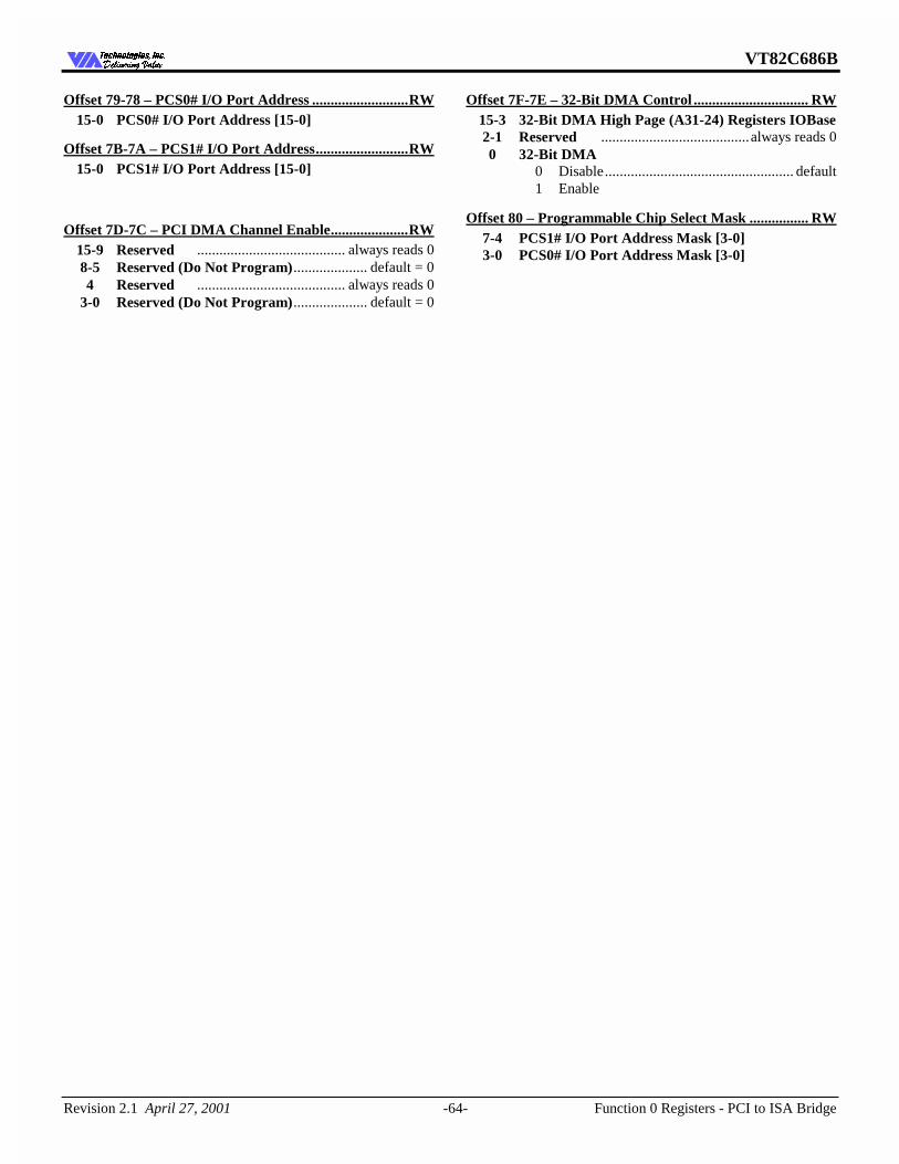
VT82C686B
Revision 2.1 April 27, 2001 -64- Function 0 Registers - PCI to ISA Bridge
7HFKQRORJLHV ,QF'HOLYHULQJ 9DOXH'HOLYHULQJ 9DOXH
Offset 79-78 – PCS0# I/O Port Address ..........................RW 15-0 PCS0# I/O Port Address [15-0]
Offset 7B-7A – PCS1# I/O Port Address.........................RW 15-0 PCS1# I/O Port Address [15-0]
Offset 7D-7C – PCI DMA Channel Enable.....................RW 15-9 Reserved ........................................ always reads 0 8-5 Reserved (Do Not Program).................... default = 0 4 Reserved ........................................ always reads 0 3-0 Reserved (Do Not Program).................... default = 0
Offset 7F-7E – 32-Bit DMA Control ............................... RW 15-3 32-Bit DMA High Page (A31-24) Registers IOBase 2-1 Reserved ........................................always reads 0 0 32-Bit DMA 0 Disable................................................... default 1 Enable
Offset 80 – Programmable Chip Select Mask ................ RW 7-4 PCS1# I/O Port Address Mask [3-0] 3-0 PCS0# I/O Port Address Mask [3-0]
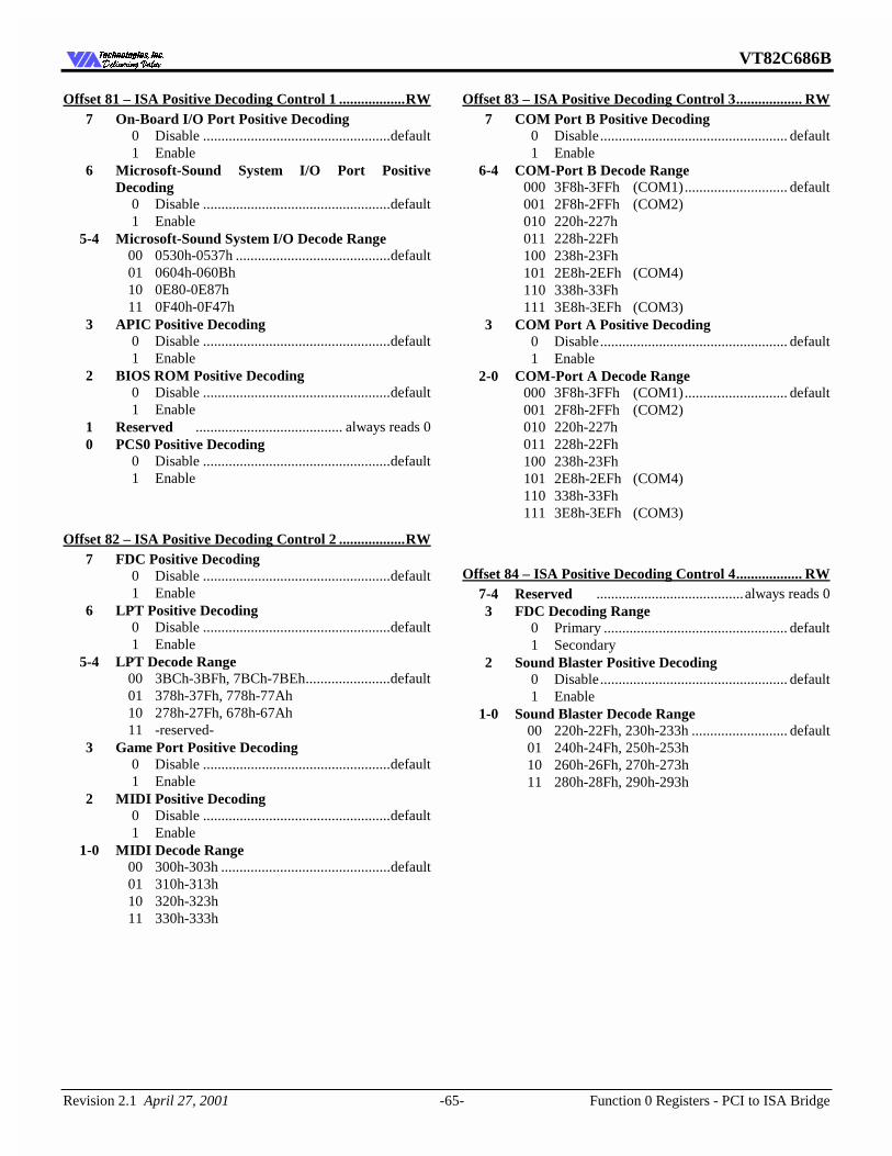
VT82C686B
Revision 2.1 April 27, 2001 -65- Function 0 Registers - PCI to ISA Bridge
7HFKQRORJLHV ,QF'HOLYHULQJ 9DOXH'HOLYHULQJ 9DOXH
Offset 81 – ISA Positive Decoding Control 1 ..................RW 7 On-Board I/O Port Positive Decoding 0 Disable ...................................................default 1 Enable 6 Microsoft-Sound System I/O Port Positive
Decoding 0 Disable ...................................................default 1 Enable 5-4 Microsoft-Sound System I/O Decode Range 00 0530h-0537h ..........................................default 01 0604h-060Bh 10 0E80-0E87h 11 0F40h-0F47h 3 APIC Positive Decoding 0 Disable ...................................................default 1 Enable 2 BIOS ROM Positive Decoding 0 Disable ...................................................default 1 Enable 1 Reserved ........................................ always reads 0 0 PCS0 Positive Decoding 0 Disable ...................................................default 1 Enable
Offset 82 – ISA Positive Decoding Control 2 ..................RW 7 FDC Positive Decoding 0 Disable ...................................................default 1 Enable 6 LPT Positive Decoding 0 Disable ...................................................default 1 Enable 5-4 LPT Decode Range 00 3BCh-3BFh, 7BCh-7BEh.......................default 01 378h-37Fh, 778h-77Ah 10 278h-27Fh, 678h-67Ah 11 -reserved- 3 Game Port Positive Decoding 0 Disable ...................................................default 1 Enable 2 MIDI Positive Decoding 0 Disable ...................................................default 1 Enable 1-0 MIDI Decode Range 00 300h-303h ..............................................default 01 310h-313h 10 320h-323h 11 330h-333h
Offset 83 – ISA Positive Decoding Control 3.................. RW 7 COM Port B Positive Decoding 0 Disable................................................... default 1 Enable 6-4 COM-Port B Decode Range 000 3F8h-3FFh (COM1)............................ default 001 2F8h-2FFh (COM2) 010 220h-227h 011 228h-22Fh 100 238h-23Fh 101 2E8h-2EFh (COM4) 110 338h-33Fh 111 3E8h-3EFh (COM3) 3 COM Port A Positive Decoding 0 Disable................................................... default 1 Enable 2-0 COM-Port A Decode Range 000 3F8h-3FFh (COM1)............................ default 001 2F8h-2FFh (COM2) 010 220h-227h 011 228h-22Fh 100 238h-23Fh 101 2E8h-2EFh (COM4) 110 338h-33Fh 111 3E8h-3EFh (COM3)
Offset 84 – ISA Positive Decoding Control 4.................. RW 7-4 Reserved ........................................always reads 0 3 FDC Decoding Range 0 Primary .................................................. default 1 Secondary 2 Sound Blaster Positive Decoding 0 Disable................................................... default 1 Enable 1-0 Sound Blaster Decode Range 00 220h-22Fh, 230h-233h .......................... default 01 240h-24Fh, 250h-253h 10 260h-26Fh, 270h-273h 11 280h-28Fh, 290h-293h
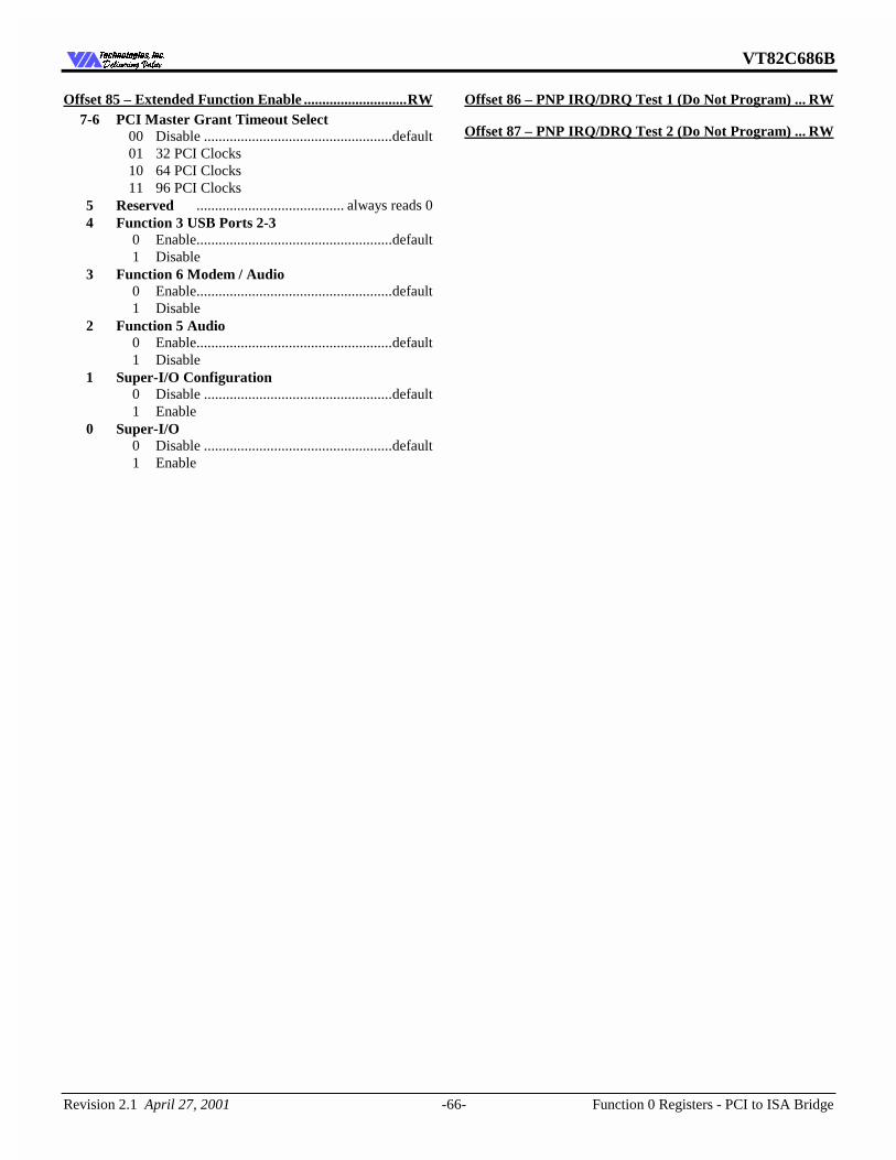
VT82C686B
Revision 2.1 April 27, 2001 -66- Function 0 Registers - PCI to ISA Bridge
7HFKQRORJLHV ,QF'HOLYHULQJ 9DOXH'HOLYHULQJ 9DOXH
Offset 85 – Extended Function Enable ............................RW 7-6 PCI Master Grant Timeout Select 00 Disable ...................................................default 01 32 PCI Clocks 10 64 PCI Clocks 11 96 PCI Clocks 5 Reserved ........................................ always reads 0 4 Function 3 USB Ports 2-3 0 Enable.....................................................default 1 Disable 3 Function 6 Modem / Audio 0 Enable.....................................................default 1 Disable 2 Function 5 Audio 0 Enable.....................................................default 1 Disable 1 Super-I/O Configuration 0 Disable ...................................................default 1 Enable 0 Super-I/O 0 Disable ...................................................default 1 Enable
Offset 86 – PNP IRQ/DRQ Test 1 (Do Not Program) ... RW
Offset 87 – PNP IRQ/DRQ Test 2 (Do Not Program) ... RW
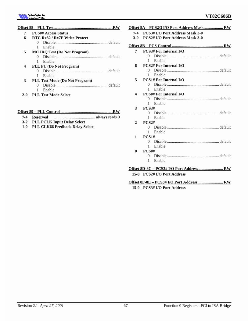
VT82C686B
Revision 2.1 April 27, 2001 -67- Function 0 Registers - PCI to ISA Bridge
7HFKQRORJLHV ,QF'HOLYHULQJ 9DOXH'HOLYHULQJ 9DOXH
Offset 88 – PLL Test .........................................................RW 7 PCS0# Access Status 6 RTC Rx32 / Rx7F Write Protect 0 Disable ...................................................default 1 Enable 5 MC IRQ Test (Do Not Program) 0 Disable ...................................................default 1 Enable 4 PLL PU (Do Not Program) 0 Disable ...................................................default 1 Enable 3 PLL Test Mode (Do Not Program) 0 Disable ...................................................default 1 Enable 2-0 PLL Test Mode Select
Offset 89 – PLL Control ...................................................RW 7-4 Reserved ........................................ always reads 0 3-2 PLL PCLK Input Delay Select 1-0 PLL CLK66 Feedback Delay Select
Offset 8A – PCS2/3 I/O Port Address Mask................... RW 7-4 PCS3# I/O Port Address Mask 3-0 3-0 PCS2# I/O Port Address Mask 3-0
Offset 8B – PCS Control .................................................. RW 7 PCS3# For Internal I/O 0 Disable................................................... default 1 Enable 6 PCS2# For Internal I/O 0 Disable................................................... default 1 Enable 5 PCS1# For Internal I/O 0 Disable................................................... default 1 Enable 4 PCS0# For Internal I/O 0 Disable................................................... default 1 Enable 3 PCS3# 0 Disable................................................... default 1 Enable 2 PCS2# 0 Disable................................................... default 1 Enable 1 PCS1# 0 Disable................................................... default 1 Enable 0 PCS0# 0 Disable................................................... default 1 Enable
Offset 8D-8C – PCS2# I/O Port Address ........................ RW 15-0 PCS2# I/O Port Address
Offset 8F-8E – PCS3# I/O Port Address......................... RW 15-0 PCS3# I/O Port Address
VT82C686B
Revision 2.1 April 27, 2001 -68- Function 1 Registers - Enhanced IDE Controller
7HFKQRORJLHV ,QF'HOLYHULQJ 9DOXH'HOLYHULQJ 9DOXH
Function 1 Registers - Enhanced IDE Controller
This Enhanced IDE controller interface is fully compatible with the SFF 8038i v.1.0 specification. There are two sets of software accessible registers -- PCI configuration registers and Bus Master IDE I/O registers. The PCI configuration registers are located in the function 1 PCI configuration space of the VT82C686B. The Bus Master IDE I/O registers are defined in the SFF8038i v1.0 specification.
PCI Configuration Space Header
Offset 1-0 - Vendor ID (1106h=VIA) ................................RO
Offset 3-2 - Device ID (0571h=IDE Controller) ...............RO
Offset 5-4 - Command.......................................................RW 15-10 Reserved ........................................ always reads 0 9 Fast Back to Back Cycles ....... default = 0 (disabled) 8 SERR# Enable ......................... default = 0 (disabled) 7 Address Stepping ....................default = 1 (enabled) A value of 1 provides additional address decode time
to IDE devices. 6 Parity Error Response ............ default = 0 (disabled) 5 VGA Palette Snoop ....................fixed at 0 (disabled) 4 Memory Write & Invalidate .....fixed at 0 (disabled) 3 Special Cycles .............................fixed at 0 (disabled) 2 Bus Master ............................. default = 0 (disabled) S/G operation can be issued only when the “Bus
Master” bit is enabled. 1 Memory Space......................... default = 0 (disabled) 0 I/O Space ............................. default = 0 (disabled) When the “I/O Space” bit is disabled, the device will
not respond to any I/O addresses for both compatible and native mode.
Offset 7-6 – Status ..............................................................RO 15 Detected Parity Error ........................ always reads 0 14 Signalled System Error...................... always reads 0 13 Received Master Abort...................... always reads 0 12 Received Target Abort ...................... always reads 0 11 Signalled Target Abort ...................... always reads 0 10-9 DEVSEL# Timing ............always reads 01 (medium) 8 Data Parity Detected.......................... always reads 0 7 Fast Back to Back .............................always reads 1 6-5 Reserved ........................................ always reads 0 4 Power Management Capabilty Ptr ..always reads 1 3-0 Reserved ........................................ always reads 0
Offset 8 - Revision ID (06) .................................................RO 0-7 Revision Code for IDE Controller Logic Block
Offset 9 - Programming Interface ................................... RW 7 Master IDE Capability........... fixed at 1 (Supported) 6-4 Reserved ........................................always reads 0 3 Programmable Indicator - Secondary ...... fixed at 1 Supports both modes (may be set to either mode by
writing bit-2) 2 Reserved ........................................always reads 0 1 Programmable Indicator - Primary .......... fixed at 1 Supports both modes (may be set to either mode by
writing bit-0) 0 Reserved ........................................always reads 0
Compatibility Mode (fixed IRQs and I/O addresses): Command Block Control Block Channel Registers Registers IRQ Pri 1F0-1F7 3F6 14 Sec 170-177 376 15
Native PCI Mode (registers are programmable in I/O space) Command Block Control Block Channel Registers Registers Pri BA @offset 10h BA @offset 14h Sec BA @offset 18h BA @offset 1Ch
Command register blocks are 8 bytes of I/O space Control registers are 4 bytes of I/O space (only byte 2 is used)
Offset A - Sub Class Code (01h=IDE Controller) ........... RO
Offset B - Base Class Code (01h=Mass Storage Ctrlr) ... RO
Offset C – Cache Line Size (00h)...................................... RO
Offset D - Latency Timer (Default=0)............................. RW
Offset E - Header Type (00h)............................................ RO
Offset F - BIST (00h) ......................................................... RO
VT82C686B
Revision 2.1 April 27, 2001 -69- Function 1 Registers - Enhanced IDE Controller
7HFKQRORJLHV ,QF'HOLYHULQJ 9DOXH'HOLYHULQJ 9DOXH
Offset 13-10 - Pri Data / Command Base Address..........RW Specifies an 8 byte I/O address space.
31-16 Reserved ..........................................always read 0 15-3 Port Address ....................................... default=01F0h 2-0 Fixed at 001b (Native Mode) ............................ fixed Fixed at 000b (Compatibility Mode)
Offset 17-14 - Pri Control / Status Base Address............RW Specifies a 4 byte I/O address space of which only the third byte is active (i.e., 3F6h for the default base address of 3F4h).
31-16 Reserved ..........................................always read 0 15-2 Port Address ....................................... default=03F4h 1-0 Fixed at 01b (Native Mode) .............................. fixed Fixed at 00b (Compatibility Mode)
Offset 1B-18 - Sec Data / Command Base Address ........RW Specifies an 8 byte I/O address space.
31-16 Reserved ..........................................always read 0 15-3 Port Address ...................................... default=0170h 2-0 Fixed at 001b (Native Mode) ............................ fixed Fixed at 000b (Compatibility Mode)
Offset 1F-1C - Sec Control / Status Base Address..........RW Specifies a 4 byte I/O address space of which only the third byte is active (i.e., 376h for the default base address of 374h).
31-16 Reserved ..........................................always read 0 15-2 Port Address ...................................... default=0374h 1-0 Fixed at 01b (Native Mode) .............................. fixed Fixed at 00b (Compatibility Mode)
Offset 23-20 - Bus Master Control Regs Base Address..RW Specifies a 16 byte I/O address space compliant with the SFF-8038i rev 1.0 specification.
31-16 Reserved ..........................................always read 0 15-4 Port Address ....................................... default=CC0h 3-0 Fixed at 0001b (Native Mode) .......................... fixed Fixed at 0000b (Compatibility Mode)
See Rx42[7-6] for Native / Compatibility mode select for the above registers
Offset 34 - Capability Pointer (C0h) ................................ RO
Offset 3C - Interrupt Line (0Eh) ...................................... RO
Offset 3D - Interrupt Pin (00h)......................................... RO 7-0 Interrupt Routing Mode 00h Legacy mode interrupt routing............... default 01h Native mode interrupt routing
Offset 3E - Min Gnt (00h) ................................................. RO
Offset 3F - Max Latency (00h).......................................... RO
VT82C686B
Revision 2.1 April 27, 2001 -70- Function 1 Registers - Enhanced IDE Controller
7HFKQRORJLHV ,QF'HOLYHULQJ 9DOXH'HOLYHULQJ 9DOXH
IDE-Controller-Specific Confiiguration Registers
Offset 40 - Chip Enable (08h)...........................................RW 7-4 Reserved ........................................ always reads 0 3-2 Reserved (Do Not Program).......R/W, default = 10b 1 Primary Channel Enable ........ default = 0 (disabled) 0 Secondary Channel Enable .... default = 0 (disabled)
Offset 41 - IDE Configuration I (02h) .............................RW 7 Primary IDE Read Prefetch Buffer 0 Disable ...................................................default 1 Enable 6 Primary IDE Post Write Buffer 0 Disable ...................................................default 1 Enable 5 Secondary IDE Read Prefetch Buffer 0 Disable ...................................................default 1 Enable 4 Secondary IDE Post Write Buffer 0 Disable ...................................................default 1 Enable 3-2 Reserved ........................................ always reads 0 1 Reserved (Do Not Program)...................... default=1 0 Reserved ........................................ always reads 0
Offset 42 - IDE Configuration II (09h)............................RW 7 Primary Channel PIO Operation Mode 0 Compatibility Mode 1 Native Mode...........................................default 6 Secondary Channel PIO Operation Mode 0 Compatibility Mode 1 Native Mode...........................................default 5-2 Reserved (Do Not Program)........ default = 000010b 1-0 DEVSEL# Timing Select ..................... default = 01b (also reflected in Rx07)
Offset 43 - FIFO Configuration (0Ah).............................RW 7-4 Reserved ........................................ always reads 0 3-2 Threshold for Primary Channel 00 1/4 01 1/2 10 3/4 .....................................................default 11 1 1-0 Threshold for Secondary Channel 00 1/4 01 1/2 10 3/4 .....................................................default 11 1
Offset 44 - Miscellaneous Control 1 (68h) ...................... RW 7 IDE Controller Max Speed 0 UDMA100............................................. default 1 UDMA66 6 Master Read Cycle IRDY# Wait States 0 0 wait states 1 1 wait state ............................................. default 5 Master Write Cycle IRDY# Wait States 0 0 wait states 1 1 wait state ............................................. default 4 PIO Read Prefetch Byte Counter 0 Disable................................................... default 1 Enable 3 Bus Master IDE Status Register Read Retry Retry bus master IDE status register read when
master write operation for DMA read is not complete 0 Disable 1 Enable .................................................... default 2 Packet Command Prefetching 0 Disable................................................... default 1 Enable 1 Reserved ........................................always reads 0 0 UltraDMA Host Must Wait for First Strobe
Before Termination 0 Enable .................................................... default 1 Disable
Offset 45 - Miscellaneous Control 2 (00h) ...................... RW 7 Reserved ........................................always reads 0 6 Interrupt Steering Swap 0 Don’t swap channel interrupts ............... default 1 Swap interrupts between the two channels 5 Reserved ........................................always reads 0 4 Rx3C Write Protect 0 Enable .................................................... default 1 Disable 3 Memory Read Multiple Command 0 Disable................................................... default 1 Enable 2 Memory Write and Invalidate Command 0 Disable................................................... default 1 Enable 1-0 Reserved ........................................always reads 0
Offset 46 - Miscellaneous Control 3 (C0h) ..................... RW 7 Primary Channel Read DMA FIFO Flush 0 Disable 1 Enable FIFO flush for Read DMA when
interrupt asserts primary channel. .......... default 6 Secondary Channel Read DMA FIFO Flush 0 Disable 1 Enable FIFO flush for Read DMA when
interrupt asserts secondary channel........ default 5-0 Reserved ........................................always reads 0
VT82C686B
Revision 2.1 April 27, 2001 -71- Function 1 Registers - Enhanced IDE Controller
7HFKQRORJLHV ,QF'HOLYHULQJ 9DOXH'HOLYHULQJ 9DOXH
Offset 4B-48 - Drive Timing Control (A8A8A8A8h)......RW The following fields define the Active Pulse Width and Recovery Time for the IDE DIOR# and DIOW# signals:
31-28 Primary Drive 0 Active Pulse Width ...... def=1010b 27-24 Primary Drive 0 Recovery Time ............. def=1000b 23-20 Primary Drive 1 Active Pulse Width ...... def=1010b 19-16 Primary Drive 1 Recovery Time ............. def=1000b 15-12 Secondary Drive 0 Active Pulse Width .. def=1010b 11-8 Secondary Drive 0 Recovery Time ......... def=1000b 7-4 Secondary Drive 1 Active Pulse Width .. def=1010b 3-0 Secondary Drive 1 Recovery Time ......... def=1000b
The actual value for each field is the encoded value in the field plus one and indicates the number of PCI clocks.
Offset 4C - Address Setup Time (FFh) ............................RW 7-6 Primary Drive 0 Address Setup Time ........ def = 11 5-4 Primary Drive 1 Address Setup Time ....... def = 11 3-2 Secondary Drive 0 Address Setup Time .... def = 11 1-0 Secondary Drive 1 Address Setup Time .... def = 11
For each field above: 00 1T 01 2T 10 3T 11 4T .....................................................default
Offset 53-50 - UltraDMA Extended Timing Control ..... RW 31 Pri Drive 0 UltraDMA-Mode Enable Method 0 Enable by using “Set Feature” command..... def 1 Enable by setting bit-30 of this register 30 Pri Drive 0 UltraDMA-Mode Enable 0 Disable................................................... default 1 Enable UltraDMA-Mode Operation 29 Pri Drive 0 Transfer Mode 0 DMA or PIO Mode ............................... default 1 UltraDMA Mode 28 Pri Drive 0 Cabal Type Reporting 0 Disable................................................... default 1 Enable 27 Reserved ........................................always reads 0 26-24 Pri Drive 0 Cycle Time (T = 10nsec) 000 2T 001 3T 010 4T 011 5T 100 6T 101 7T 110 8T 111 9T .................................................... default
23 Pri Drive 1 UltraDMA-Mode Enable Method 22 Pri Drive 1 UltraDMA-Mode Enable 21 Pri Drive 1 Transfer Mode 20 Pri Drive 1 Cabal Type Reporting 0 Disable................................................... default 1 Enable 19 Reserved ........................................always reads 0 18-16 Pri Drive 1 Cycle Time.......... (see above for default)
15 Sec Drive 0 UltraDMA-Mode Enable Method 14 Sec Drive 0 UltraDMA-Mode Enable 13 Sec Drive 0 Transfer Mode 12 Sec Drive 0 Cabal Type Reporting 0 Disable................................................... default 1 Enable 11 Reserved ........................................always reads 0 10-8 Sec Drive 0 Cycle Time ......... (see above for default)
7 Sec Drive 1 UltraDMA-Mode Enable Method 6 Sec Drive 1 UltraDMA-Mode Enable 5 Sec Drive 1 Transfer Mode 4 Sec Drive 1 Cabal Type Reporting 0 Disable................................................... default 1 Enable 3 Reserved ........................................always reads 0 2-0 Sec Drive 1 Cycle Time ......... (see above for default)
Each byte defines UltraDMA operation for the indicated drive. The bit definitions are the same within each byte.
VT82C686B
Revision 2.1 April 27, 2001 -72- Function 1 Registers - Enhanced IDE Controller
7HFKQRORJLHV ,QF'HOLYHULQJ 9DOXH'HOLYHULQJ 9DOXH
Offset 54 – UltraDMA FIFO Control (04h) ....................RW 7-5 Reserved ........................................ always reads 0 4 One Frame For Each PCI Request For IDE PCI
Master Cycles 0 Disable ...................................................default 1 Enable 3 Reserved ........................................ always reads 0 2 Change Drive to Clear All FIFO & Internal States 0 Disable 1 Enable.....................................................default 1 Reserved ........................................ always reads 0 0 Complete DMA Cycle with Transfer Size Less
Than FIFO Size 0 Enable.....................................................default 1 Disable
Offset 61-60 - Primary Sector Size (0200h).....................RW 15-12 Reserved ........................................ always reads 0 11-0 Number of Bytes Per Sector ... def=200h (512 bytes)
Offset 69-68 - Secondary Sector Size (0200h) .................RW 15-12 Reserved ........................................ always reads 0 11-0 Number of Bytes Per Sector ... def=200h (512 bytes)
Offset 70 – Primary IDE Status....................................... RW 7 Interrupt Status 6 Prefetch Buffer Status 5 Post Write Buffer Status 4 DMA Read Prefetch Status 3 DMA Write Prefetch Status 2 S/G Operation Complete 1 FIFO Empty Status 0 Response to External DMAREQ
Offset 71 – Primary Interrupt Control ........................... RW 7-1 Reserved ........................................always reads 0 0 Flush FIFO Before Generating IDE Interrupt 0 Disable................................................... default 1 Enable
Offset 78 – Secondary IDE Status ................................... RW 7 Interrupt Status 6 Prefetch Buffer Status 5 Post Write Buffer Status 4 DMA Read Prefetch Status 3 DMA Write Prefetch Status 2 S/G Operation Complete 1 FIFO Empty Status 0 Response to External DMAREQ
Offset 79 - Secondary Interrupt Control ........................ RW 7-1 Reserved ........................................always reads 0 0 Flush FIFO Before Generating IDE Interrupt 0 Disable................................................... default 1 Enable
Offset 83-80 – Primary S/G Descriptor Address............ RW
Offset 8B-88 – Secondary S/G Descriptor Address........ RW
Offset C3-C0 – PCI PM Block 1....................................... RO 31-0 PCI PM Block 1 ................. always reads 0002 0001h
Offset C7-C4 – PCI PM Block 2....................................... RO 31-2 Reserved ........................................always reads 0 1-0 Power State 00 On .................................................... default 01 Off 1x -reserved-
VT82C686B
Revision 2.1 April 27, 2001 -73- Function 1 Registers - Enhanced IDE Controller
7HFKQRORJLHV ,QF'HOLYHULQJ 9DOXH'HOLYHULQJ 9DOXH
IDE I/O Registers
These registers are compliant with the SFF 8038I v1.0 standard. Refer to the SFF 8038I v1.0 specification for further details.
I/O Offset 0 - Primary Channel Command
I/O Offset 2 - Primary Channel Status
I/O Offset 4-7 - Primary Channel PRD Table Address
I/O Offset 8 - Secondary Channel Command
I/O Offset A - Secondary Channel Status
I/O Offset C-F - Secondary Channel PRD Table Address
VT82C686B
Revision 2.1 April 27, 2001 -74- Function 2 Registers - USB Controller Ports 0-1
7HFKQRORJLHV ,QF'HOLYHULQJ 9DOXH'HOLYHULQJ 9DOXH
Function 2 Registers - USB Controller Ports 0-1
This Universal Serial Bus host controller interface is fully compatible with UHCI specification v1.1. There are two sets of software accessible registers: PCI configuration registers and USB I/O registers. The PCI configuration registers are located in the function 2 PCI configuration space of the VT82C686B. The USB I/O registers are defined in UHCI specification v1.1. The registers in this function control USB ports 0-1 (see function 3 for ports 2-3).
PCI Configuration Space Header
Offset 1-0 - Vendor ID .......................................................RO 0-7 Vendor ID ................. (1106h = VIA Technologies)
Offset 3-2 - Device ID.........................................................RO 0-7 Device ID (3038h = VT82C686B USB Controller)
Offset 5-4 – Command (0000h) ........................................RW 15-8 Reserved ........................................ always reads 0 7 Address Stepping ...................... default=0 (disabled) 6 Reserved (parity error response) ..................fixed at 0 5 Reserved (VGA palette snoop) ....................fixed at 0 4 Memory Write and Invalidate . default=0 (disabled) 3 Reserved (special cycle monitoring) ............fixed at 0 2 Bus Master ............................... default=0 (disabled) 1 Memory Space........................... default=0 (disabled) 0 I/O Space ............................... default=0 (disabled)
Offset 7-6 – Status (0210h) ............................................RWC 15 Reserved (detected parity error).......... always reads 0 14 Signalled System Error.............................. default=0 13 Received Master Abort.............................. default=0 12 Received Target Abort .............................. default=0 11 Signalled Target Abort .............................. default=0 10-9 DEVSEL# Timing 00 Fast 01 Medium ......................................default (fixed) 10 Slow 11 Reserved 8-5 Reserved ........................................ always reads 0 4 Pwr Mgmt Extended Capabilties...... always reads 1 3-0 Reserved ........................................ always reads 0
Offset 8 - Revision ID (nnh) .............................................. RO 7-0 Silicon Revision Code (0 indicates first silicon) 06h Corresponds to Chip Revision D
Offset 9 - Programming Interface (00h) .......................... RO
Offset A - Sub Class Code (03h=USB Controller) .......... RO
Offset B - Base Class Code (0Ch=Serial Bus Controller)RO
Offset C – Cache Line Size (00h)...................................... RO
Offset D - Latency Timer ................................................. RW 7-0 Timer Value ..........................................default = 16h
Offset E - Header Type (00h)............................................ RO
Offset F - BIST (00h) ......................................................... RO
Offset 23-20 - USB I/O Register Base Address............... RW 31-16 Reserved ........................................always reads 0 15-5 USB I/O Register Base Address. Port Address for
the base of the 32-byte USB I/O Register block, corresponding to AD[15:5]
4-0 00001b
Offset 34 – USB Power Management Capabilities (80h) RO
Offset 3C - Interrupt Line (00h)...................................... RW 7-4 Reserved ........................................always reads 0 3-0 USB Interrupt Routing ........................default = 16h 0000 Disable................................................... default 0001 IRQ1 0010 Reserved 0011 IRQ3 0100 IRQ4 0101 IRQ5 0110 IRQ6 0111 IRQ7 1000 IRQ8 1001 IRQ9 1010 IRQ10 1011 IRQ11 1100 IRQ12 1101 IRQ13 1110 IRQ14 1111 Disable
Offset 3D - Interrupt Pin (04h)......................................... RO
VT82C686B
Revision 2.1 April 27, 2001 -75- Function 2 Registers - USB Controller Ports 0-1
7HFKQRORJLHV ,QF'HOLYHULQJ 9DOXH'HOLYHULQJ 9DOXH
USB-Specific Configuration Registers
Offset 40 - Miscellaneous Control 1.................................RW 7 PCI Memory Command Option 0 Support Memory-Read-Line, Memory-Read-
Multiple, & Memory-Write-&-Invalidate.... def 1 Only support Mem Read, Mem Write Cmds 6 Babble Option 0 Automatically disable babbled port when EOF
babble occurs..........................................default 1 Don’t disable babbled port 5 PCI Parity Check Option 0 Disable PERR# generation.....................default 1 Enable parity check and PERR# generation 4 Frame Interval Select 0 1 ms frame..............................................default 1 0.1 ms frame 3 USB Data Length Option 0 Support TD length up to 1280................default 1 Support TD length up to 1023 2 USB Power Management 0 Disable USB power management...........default 1 Enable USB power management 1 DMA Option 0 8 DW burst access with better FIFO latencydef 1 16 DW burst access (original performance) 0 PCI Wait States 0 Zero wait ................................................default 1 One wait
Offset 41 - Miscellaneous Control 2 ................................ RW 7 USB 1.1 Improvement for EOP 0 USB Specification 1.1 Compliant.......... default If a bit stuffing error occurs before EOP, the
receiver will accept the packet 1 USB Specification 1.0 Compliant If a bit stuffing error occurs before EOP, the
receiver will ignore the packet 6-5 Reserved (Do Not Program) ....................default = 0 4 Hold PCI Request for Successive Accesses 0 Disable 1 Enable .................................................... default Setting this bit to “enable” causes the system to treat
the USB request as higher priority 3 Frame Counter Test Mode 0 Disable................................................... default 1 Enable 2 Trap Option 0 Set trap 60/64 status bits only when trap 60/64
enable bits are set. ................................. default 1 Set trap 60/64 status bits without checking
enable bits 1 A20gate Pass Through Option 0 Pass through A20GATE command sequence
defined in UHCI .................................... default 1 Don’t pass through Write I/O port 64 (ff) 0 USB IRQ Test Mode 0 Normal Operation .................................. default 1 Generate USB IRQ
VT82C686B
Revision 2.1 April 27, 2001 -76- Function 2 Registers - USB Controller Ports 0-1
7HFKQRORJLHV ,QF'HOLYHULQJ 9DOXH'HOLYHULQJ 9DOXH
Offset 42 - FIFO Control ..................................................RW 7-4 Reserved ........................................ always reads 0 3-2 Reserved (Do Not Program).................... default = 0 1-0 Release Continuous REQ After “N” PCICLKs 00 Do Not Release ......................................default 01 N = 32 PCICLKs 10 N = 64 PCICLKs 11 N = 96 PCICLKs
Offset 60 - Serial Bus Release Number.............................RO 7-0 Release Number.............................. always reads 10h
Offset 83-80 – PM Capability............................................RO 31-0 PM Capability .................... always reads 00020001h
Offset 84 – PM Capability Status ....................................RW 7-0 PM Capability Status........................... default = 00h Supports 00h (Off) and 11h (On) only
Offset C1-C0 - Legacy Support.........................................RO 15-0 UHCI v1.1 Compliant ................ always reads 2000h
USB I/O Registers
These registers are compliant with the UHCI v1.1 standard. Refer to the UHCI v1.1 specification for further details.
I/O Offset 1-0 - USB Command
I/O Offset 3-2 - USB Status
I/O Offset 5-4 - USB Interrupt Enable
I/O Offset 7-6 - Frame Number
I/O Offset B-8 - Frame List Base Address
I/O Offset 0C - Start Of Frame Modify
I/O Offset 11-10 - Port 0 Status / Control
I/O Offset 13-12 - Port 1 Status / Control
VT82C686B
Revision 2.1 April 27, 2001 -77- Function 3 Registers - USB Controller Ports 2-3
7HFKQRORJLHV ,QF'HOLYHULQJ 9DOXH'HOLYHULQJ 9DOXH
Function 3 Registers - USB Controller Ports 2-3
This Universal Serial Bus host controller interface is fully compatible with UHCI specification v1.1. There are two sets of software accessible registers: PCI configuration registers and USB I/O registers. The PCI configuration registers are located in the function 3 PCI configuration space of the VT82C686B. The USB I/O registers are defined in UHCI specification v1.1. The registers in this function control USB ports 2-3 (see function 2 for ports 0-1).
PCI Configuration Space Header
Offset 1-0 - Vendor ID .......................................................RO 0-7 Vendor ID ................. (1106h = VIA Technologies)
Offset 3-2 - Device ID.........................................................RO 0-7 Device ID (3038h = VT82C686B USB Controller)
Offset 5-4 – Command (0000h) ........................................RW 15-8 Reserved ........................................ always reads 0 7 Address Stepping ...................... default=0 (disabled) 6 Reserved (parity error response) ..................fixed at 0 5 Reserved (VGA palette snoop) ....................fixed at 0 4 Memory Write and Invalidate . default=0 (disabled) 3 Reserved (special cycle monitoring) ............fixed at 0 2 Bus Master ............................... default=0 (disabled) 1 Memory Space........................... default=0 (disabled) 0 I/O Space ............................... default=0 (disabled)
Offset 7-6 – Status (0210h) ............................................RWC 15 Reserved (detected parity error).......... always reads 0 14 Signalled System Error.............................. default=0 13 Received Master Abort.............................. default=0 12 Received Target Abort .............................. default=0 11 Signalled Target Abort .............................. default=0 10-9 DEVSEL# Timing 00 Fast 01 Medium ......................................default (fixed) 10 Slow 11 Reserved 8-5 Reserved ........................................ always reads 0 4 Pwr Mgmt Extended Capabilties...... always reads 1 3-0 Reserved ........................................ always reads 0
Offset 8 - Revision ID (nnh) .............................................. RO 7-0 Silicon Revision Code (0 indicates first silicon)
Offset 9 - Programming Interface (00h) .......................... RO
Offset A - Sub Class Code (03h=USB Controller) .......... RO
Offset B - Base Class Code (0Ch=Serial Bus Controller)RO
Offset C – Cache Line Size (00h)...................................... RO
Offset D - Latency Timer ................................................. RW 7-0 Timer Value ..........................................default = 16h
Offset E - Header Type (00h)............................................ RO
Offset F - BIST (00h) ......................................................... RO
Offset 23-20 - USB I/O Register Base Address............... RW 31-16 Reserved ........................................always reads 0 15-5 USB I/O Register Base Address. Port Address for
the base of the 32-byte USB I/O Register block, corresponding to AD[15:5]
4-0 00001b
Offset 34 – USB Power Management Capabilities (80h) RO
Offset 3C - Interrupt Line (00h)...................................... RW 7-4 Reserved ........................................always reads 0 3-0 USB Interrupt Routing ........................default = 16h 0000 Disable................................................... default 0001 IRQ1 0010 Reserved 0011 IRQ3 0100 IRQ4 0101 IRQ5 0110 IRQ6 0111 IRQ7 1000 IRQ8 1001 IRQ9 1010 IRQ10 1011 IRQ11 1100 IRQ12 1101 IRQ13 1110 IRQ14 1111 Disable
Offset 3D - Interrupt Pin (04h)......................................... RO

VT82C686B
Revision 2.1 April 27, 2001 -78- Function 3 Registers - USB Controller Ports 2-3
7HFKQRORJLHV ,QF'HOLYHULQJ 9DOXH'HOLYHULQJ 9DOXH
USB-Specific Configuration Registers
Offset 40 - Miscellaneous Control 1.................................RW 7 PCI Memory Command Option 0 Support Memory-Read-Line, Memory-Read-
Multiple, & Memory-Write-&-Invalidate.... def 1 Only support Mem Read, Mem Write Cmds 6 Babble Option 0 Automatically disable babbled port when EOF
babble occurs..........................................default 1 Don’t disable babbled port 5 PCI Parity Check Option 0 Disable PERR# generation.....................default 1 Enable parity check and PERR# generation 4 Frame Interval Select 0 1 ms frame..............................................default 1 0.1 ms frame 3 USB Data Length Option 0 Support TD length up to 1280................default 1 Support TD length up to 1023 2 USB Power Management 0 Disable USB power management...........default 1 Enable USB power management 1 DMA Option 0 8 DW burst access with better FIFO latencydef 1 16 DW burst access (original performance) 0 PCI Wait States 0 Zero wait ................................................default 1 One wait
Offset 41 - Miscellaneous Control 2 ................................ RW 7 USB 1.1 Improvement for EOP 0 USB Specification 1.1 Compliant.......... default If a bit stuffing error occurs before EOP, the
receiver will accept the packet 1 USB Specification 1.0 Compliant If a bit stuffing error occurs before EOP, the
receiver will ignore the packet 6-5 Reserved (Do Not Program) ....................default = 0 4 Hold PCI Request for Successive Accesses 0 Disable 1 Enable .................................................... default Setting this bit to “enable” causes the system to treat
the USB request as higher priority 3 Frame Counter Test Mode 0 Disable................................................... default 1 Enable 2 Trap Option 0 Set trap 60/64 status bits only when trap 60/64
enable bits are set. ................................. default 1 Set trap 60/64 status bits without checking
enable bits 1 A20gate Pass Through Option 0 Pass through A20GATE command sequence
defined in UHCI .................................... default 1 Don’t pass through Write I/O port 64 (ff) 0 USB IRQ Test Mode 0 Normal Operation .................................. default 1 Generate USB IRQ
VT82C686B
Revision 2.1 April 27, 2001 -79- Function 3 Registers - USB Controller Ports 2-3
7HFKQRORJLHV ,QF'HOLYHULQJ 9DOXH'HOLYHULQJ 9DOXH
Offset 42 - FIFO Control ..................................................RW 7-4 Reserved ........................................ always reads 0 3-2 Reserved (Do Not Program).................... default = 0 1-0 Release Continuous REQ After “N” PCICLKs 00 Do Not Release ......................................default 01 N = 32 PCICLKs 10 N = 64 PCICLKs 11 N = 96 PCICLKs
Offset 60 - Serial Bus Release Number.............................RO 7-0 Release Number.............................. always reads 10h
Offset 83-80 – PM Capability............................................RO 31-0 PM Capability .................... always reads 00020001h
Offset 84 – PM Capability Status ....................................RW 7-0 PM Capability Status.......supports 00h and 11h only
Offset C1-C0 - Legacy Support.........................................RO 15-0 UHCI v1.1 Compliant ................ always reads 2000h
USB I/O Registers
These registers are compliant with the UHCI v1.1 standard. Refer to the UHCI v1.1 specification for further details.
I/O Offset 1-0 - USB Command
I/O Offset 3-2 - USB Status
I/O Offset 5-4 - USB Interrupt Enable
I/O Offset 7-6 - Frame Number
I/O Offset B-8 - Frame List Base Address
I/O Offset 0C - Start Of Frame Modify
I/O Offset 11-10 - Port 0 Status / Control
I/O Offset 13-12 - Port 1 Status / Control
VT82C686B
Revision 2.1 April 27, 2001 -80- Function 4 Regs - Power Management, SMBus and HWM
7HFKQRORJLHV ,QF'HOLYHULQJ 9DOXH'HOLYHULQJ 9DOXH
Function 4 Regs - Power Management, SMBus and HWM
This section describes the ACPI (Advanced Configuration and Power Interface) Power Management system of the VT82C686B which includes a System Management Bus (SMBus) interface controller and Hardware Monitoring (HWM) subsystem. The power management system of the VT82C686B supports both ACPI and legacy power management functions and is compatible with the APM v1.2 and ACPI v1.0 specifications.
PCI Configuration Space Header
Offset 1-0 - Vendor ID .......................................................RO 0-7 Vendor ID ................. (1106h = VIA Technologies)
Offset 3-2 - Device ID.........................................................RO 0-7 Device ID ................ (3057h = ACPI Power Mgmt)
Offset 5-4 - Command.......................................................RW 15-8 Reserved ........................................ always reads 0 7 Address Stepping ........................................fixed at 0 6 Reserved (parity error response) ..................fixed at 0 5 Reserved (VGA palette snoop) ....................fixed at 0 4 Memory Write and Invalidate ...................fixed at 0 3 Reserved (special cycle monitoring) ............fixed at 0 2 Bus Master .................................................fixed at 0 1 Memory Space.............................................fixed at 0 0 I/O Space .................................................fixed at 0
Offset 7-6 - Status...........................................................RWC 15 Detected Parity Error ........................ always reads 0 14 Signalled System Error...................... always reads 0 13 Received Master Abort...................... always reads 0 12 Received Target Abort ...................... always reads 0 11 Signalled Target Abort ...................... always reads 0 10-9 DEVSEL# Timing 00 Fast 01 Medium .....................................default (fixed) 10 Slow 11 Reserved 8 Data Parity Detected.......................... always reads 0 7 Fast Back to Back Capable ............... always reads 1 6-5 Reserved ........................................ always reads 0 4 Pwr Mgmt Extended Capabilities..... always reads 1 3-0 Reserved ........................................ always reads 0
Offset 8 - Revision ID (nnh) .............................................. RO 7-0 Silicon Revision Code
Offset 9 - Programming Interface (00h) .......................... RO The value returned by this register may be changed by writing the desired value to PCI Configuration Function 4 offset 61h.
Offset A - Sub Class Code (00h) ....................................... RO The value returned by this register may be changed by writing the desired value to PCI Configuration Function 4 offset 62h.
Offset B - Base Class Code (00h) ...................................... RO The value returned by this register may be changed by writing the desired value to PCI Configuration Function 4 offset 63h.
Offset 0D - Latency Timer ............................................... RW 7-0 Timer Value ..............................................default = 0
Offset 0E - Header Type (00h).......................................... RO
Offset 34 –Pwr Mgmt Extended Capabilities Ptr (68h).. RO
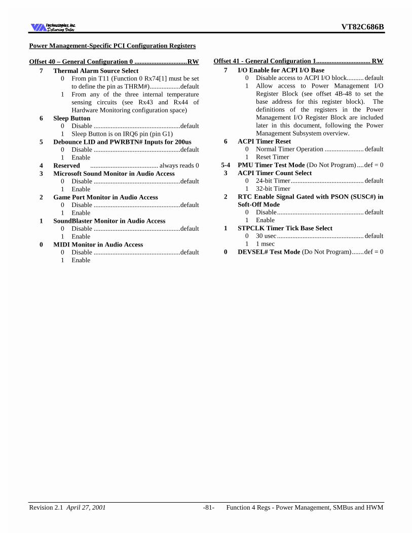
VT82C686B
Revision 2.1 April 27, 2001 -81- Function 4 Regs - Power Management, SMBus and HWM
7HFKQRORJLHV ,QF'HOLYHULQJ 9DOXH'HOLYHULQJ 9DOXH
Power Management-Specific PCI Configuration Registers
Offset 40 – General Configuration 0 ...............................RW 7 Thermal Alarm Source Select 0 From pin T11 (Function 0 Rx74[1] must be set
to define the pin as THRM#)..................default 1 From any of the three internal temperature
sensing circuits (see Rx43 and Rx44 of Hardware Monitoring configuration space)
6 Sleep Button 0 Disable ...................................................default 1 Sleep Button is on IRQ6 pin (pin G1) 5 Debounce LID and PWRBTN# Inputs for 200us 0 Disable ...................................................default 1 Enable 4 Reserved ........................................ always reads 0 3 Microsoft Sound Monitor in Audio Access 0 Disable ...................................................default 1 Enable 2 Game Port Monitor in Audio Access 0 Disable ...................................................default 1 Enable 1 SoundBlaster Monitor in Audio Access 0 Disable ...................................................default 1 Enable 0 MIDI Monitor in Audio Access 0 Disable ...................................................default 1 Enable
Offset 41 - General Configuration 1................................ RW 7 I/O Enable for ACPI I/O Base 0 Disable access to ACPI I/O block.......... default 1 Allow access to Power Management I/O
Register Block (see offset 4B-48 to set the base address for this register block). The definitions of the registers in the Power Management I/O Register Block are included later in this document, following the Power Management Subsystem overview.
6 ACPI Timer Reset 0 Normal Timer Operation ....................... default 1 Reset Timer 5-4 PMU Timer Test Mode (Do Not Program) ....def = 0 3 ACPI Timer Count Select 0 24-bit Timer........................................... default 1 32-bit Timer 2 RTC Enable Signal Gated with PSON (SUSC#) in
Soft-Off Mode 0 Disable................................................... default 1 Enable 1 STPCLK Timer Tick Base Select 0 30 usec ................................................... default 1 1 msec 0 DEVSEL# Test Mode (Do Not Program).......def = 0
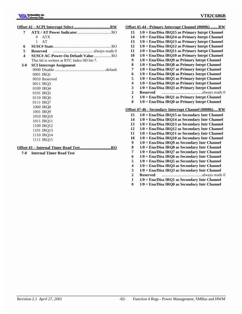
VT82C686B
Revision 2.1 April 27, 2001 -82- Function 4 Regs - Power Management, SMBus and HWM
7HFKQRORJLHV ,QF'HOLYHULQJ 9DOXH'HOLYHULQJ 9DOXH
Offset 42 - ACPI Interrupt Select ....................................RW 7 ATX / AT Power Indicator.................................. RO 0 ATX 1 AT 6 SUSC# State.......................................................... RO 5 Reserved ........................................ always reads 0 4 SUSC# AC-Power-On Default Value ................. RO This bit is written at RTC Index 0D bit-7. 3-0 SCI Interrupt Assignment 0000 Disable ...................................................default 0001 IRQ1 0010 Reserved 0011 IRQ3 0100 IRQ4 0101 IRQ5 0110 IRQ6 0111 IRQ7 1000 IRQ8 1001 IRQ9 1010 IRQ10 1011 IRQ11 1100 IRQ12 1101 IRQ13 1110 IRQ14 1111 IRQ15
Offset 43 – Internal Timer Read Test...............................RO 7-0 Internal Timer Read Test
Offset 45-44 - Primary Interrupt Channel (0000h) ....... RW 15 1/0 = Ena/Disa IRQ15 as Primary Intrpt Channel 14 1/0 = Ena/Disa IRQ14 as Primary Intrpt Channel 13 1/0 = Ena/Disa IRQ13 as Primary Intrpt Channel 12 1/0 = Ena/Disa IRQ12 as Primary Intrpt Channel 11 1/0 = Ena/Disa IRQ11 as Primary Intrpt Channel 10 1/0 = Ena/Disa IRQ10 as Primary Intrpt Channel 9 1/0 = Ena/Disa IRQ9 as Primary Intrpt Channel 8 1/0 = Ena/Disa IRQ8 as Primary Intrpt Channel 7 1/0 = Ena/Disa IRQ7 as Primary Intrpt Channel 6 1/0 = Ena/Disa IRQ6 as Primary Intrpt Channel 5 1/0 = Ena/Disa IRQ5 as Primary Intrpt Channel 4 1/0 = Ena/Disa IRQ4 as Primary Intrpt Channel 3 1/0 = Ena/Disa IRQ3 as Primary Intrpt Channel 2 Reserved ........................................always reads 0 1 1/0 = Ena/Disa IRQ1 as Primary Intrpt Channel 0 1/0 = Ena/Disa IRQ0 as Primary Intrpt Channel
Offset 47-46 - Secondary Interrupt Channel (0000h).... RW 15 1/0 = Ena/Disa IRQ15 as Secondary Intr Channel 14 1/0 = Ena/Disa IRQ14 as Secondary Intr Channel 13 1/0 = Ena/Disa IRQ13 as Secondary Intr Channel 12 1/0 = Ena/Disa IRQ12 as Secondary Intr Channel 11 1/0 = Ena/Disa IRQ11 as Secondary Intr Channel 10 1/0 = Ena/Disa IRQ10 as Secondary Intr Channel 9 1/0 = Ena/Disa IRQ9 as Secondary Intr Channel 8 1/0 = Ena/Disa IRQ8 as Secondary Intr Channel 7 1/0 = Ena/Disa IRQ7 as Secondary Intr Channel 6 1/0 = Ena/Disa IRQ6 as Secondary Intr Channel 5 1/0 = Ena/Disa IRQ5 as Secondary Intr Channel 4 1/0 = Ena/Disa IRQ4 as Secondary Intr Channel 3 1/0 = Ena/Disa IRQ3 as Secondary Intr Channel 2 Reserved ........................................always reads 0 1 1/0 = Ena/Disa IRQ1 as Secondary Intr Channel 0 1/0 = Ena/Disa IRQ0 as Secondary Intr Channel
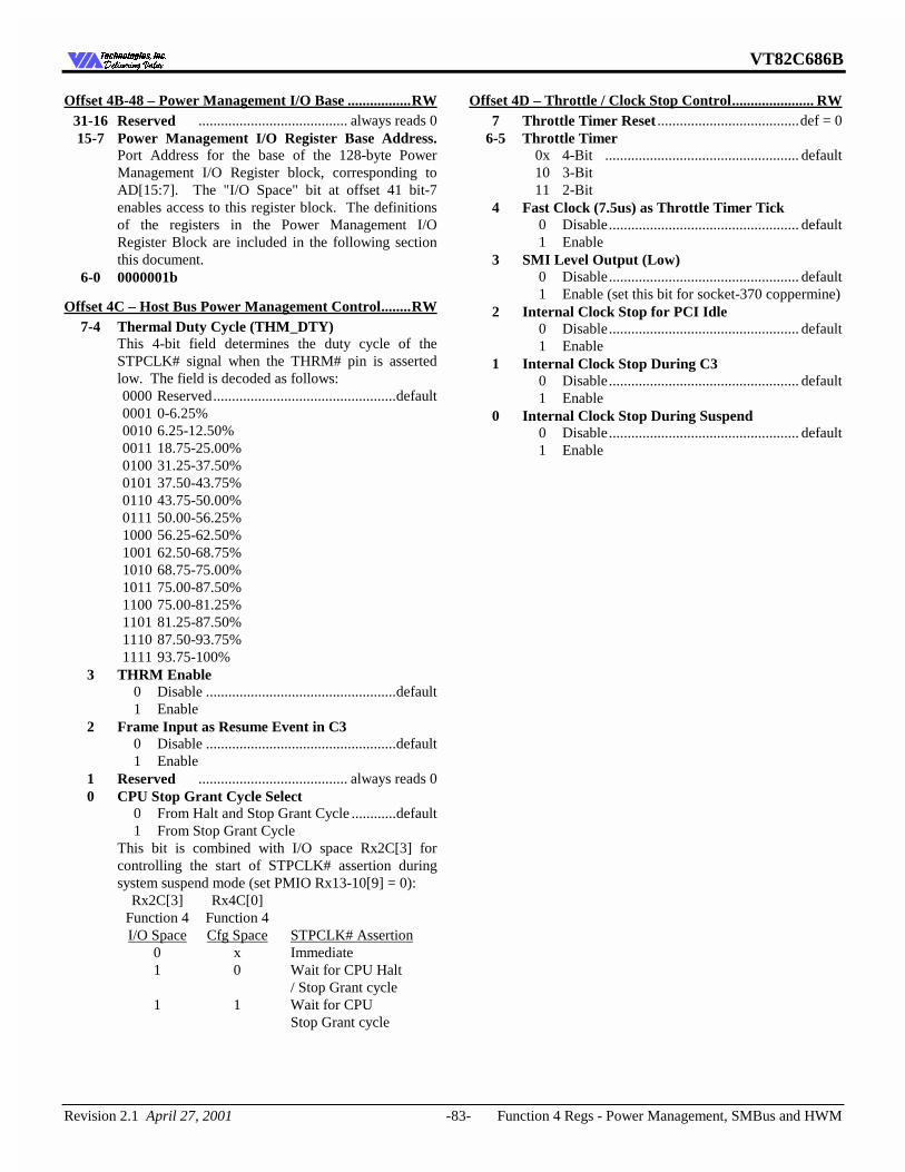
VT82C686B
Revision 2.1 April 27, 2001 -83- Function 4 Regs - Power Management, SMBus and HWM
7HFKQRORJLHV ,QF'HOLYHULQJ 9DOXH'HOLYHULQJ 9DOXH
Offset 4B-48 – Power Management I/O Base .................RW 31-16 Reserved ........................................ always reads 0 15-7 Power Management I/O Register Base Address.
Port Address for the base of the 128-byte Power Management I/O Register block, corresponding to AD[15:7]. The "I/O Space" bit at offset 41 bit-7 enables access to this register block. The definitions of the registers in the Power Management I/O Register Block are included in the following section this document.
6-0 0000001b
Offset 4C – Host Bus Power Management Control........RW 7-4 Thermal Duty Cycle (THM_DTY) This 4-bit field determines the duty cycle of the
STPCLK# signal when the THRM# pin is asserted low. The field is decoded as follows:
0000 Reserved.................................................default 0001 0-6.25% 0010 6.25-12.50% 0011 18.75-25.00% 0100 31.25-37.50% 0101 37.50-43.75% 0110 43.75-50.00% 0111 50.00-56.25% 1000 56.25-62.50% 1001 62.50-68.75% 1010 68.75-75.00% 1011 75.00-87.50% 1100 75.00-81.25% 1101 81.25-87.50% 1110 87.50-93.75% 1111 93.75-100% 3 THRM Enable 0 Disable ...................................................default 1 Enable 2 Frame Input as Resume Event in C3 0 Disable ...................................................default 1 Enable 1 Reserved ........................................ always reads 0 0 CPU Stop Grant Cycle Select 0 From Halt and Stop Grant Cycle ............default 1 From Stop Grant Cycle This bit is combined with I/O space Rx2C[3] for
controlling the start of STPCLK# assertion during system suspend mode (set PMIO Rx13-10[9] = 0):
Rx2C[3] Rx4C[0] Function 4 Function 4 I/O Space Cfg Space STPCLK# Assertion 0 x Immediate 1 0 Wait for CPU Halt / Stop Grant cycle 1 1 Wait for CPU Stop Grant cycle
Offset 4D – Throttle / Clock Stop Control...................... RW 7 Throttle Timer Reset ......................................def = 0 6-5 Throttle Timer 0x 4-Bit .................................................... default 10 3-Bit 11 2-Bit 4 Fast Clock (7.5us) as Throttle Timer Tick 0 Disable................................................... default 1 Enable 3 SMI Level Output (Low) 0 Disable................................................... default 1 Enable (set this bit for socket-370 coppermine) 2 Internal Clock Stop for PCI Idle 0 Disable................................................... default 1 Enable 1 Internal Clock Stop During C3 0 Disable................................................... default 1 Enable 0 Internal Clock Stop During Suspend 0 Disable................................................... default 1 Enable
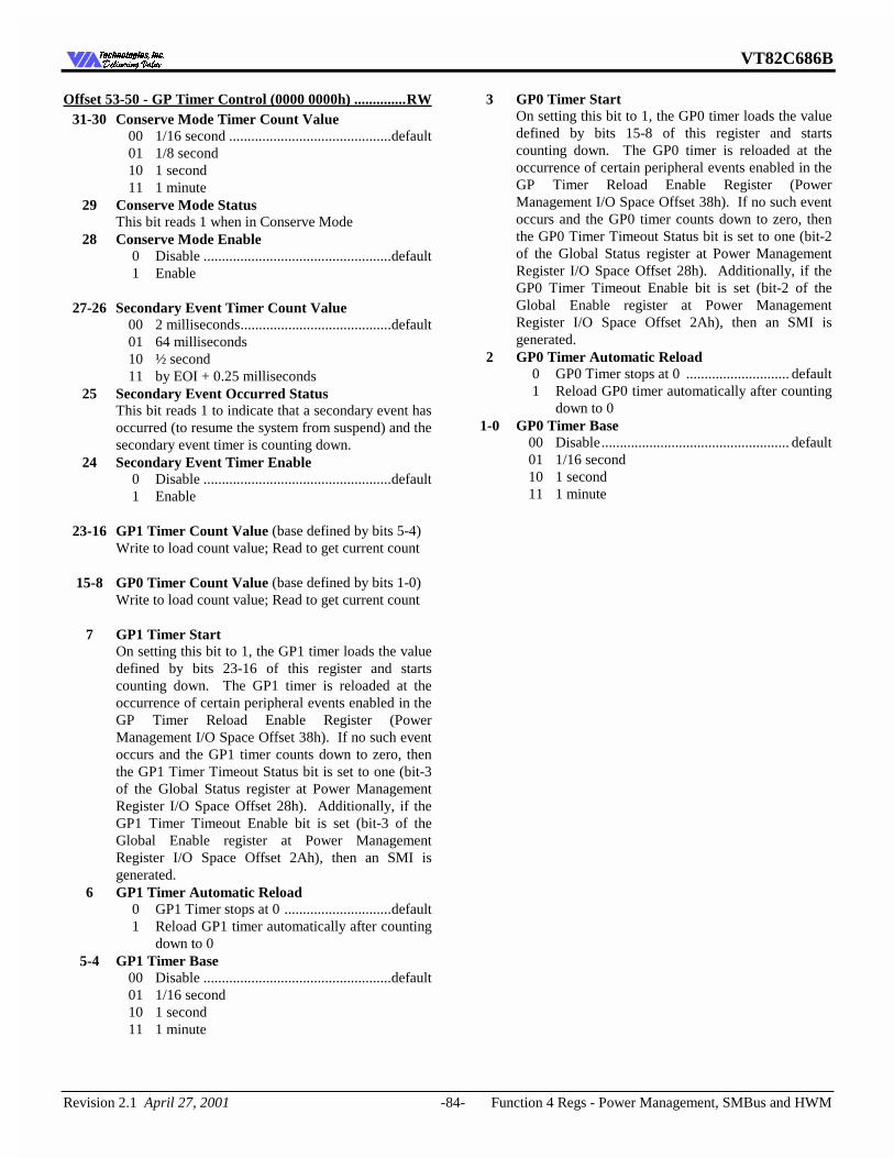
VT82C686B
Revision 2.1 April 27, 2001 -84- Function 4 Regs - Power Management, SMBus and HWM
7HFKQRORJLHV ,QF'HOLYHULQJ 9DOXH'HOLYHULQJ 9DOXH
Offset 53-50 - GP Timer Control (0000 0000h) ..............RW 31-30 Conserve Mode Timer Count Value 00 1/16 second ............................................default 01 1/8 second 10 1 second 11 1 minute 29 Conserve Mode Status This bit reads 1 when in Conserve Mode 28 Conserve Mode Enable 0 Disable ...................................................default 1 Enable 27-26 Secondary Event Timer Count Value 00 2 milliseconds.........................................default 01 64 milliseconds 10 ½ second 11 by EOI + 0.25 milliseconds 25 Secondary Event Occurred Status This bit reads 1 to indicate that a secondary event has
occurred (to resume the system from suspend) and the secondary event timer is counting down.
24 Secondary Event Timer Enable 0 Disable ...................................................default 1 Enable 23-16 GP1 Timer Count Value (base defined by bits 5-4) Write to load count value; Read to get current count 15-8 GP0 Timer Count Value (base defined by bits 1-0) Write to load count value; Read to get current count 7 GP1 Timer Start On setting this bit to 1, the GP1 timer loads the value
defined by bits 23-16 of this register and starts counting down. The GP1 timer is reloaded at the occurrence of certain peripheral events enabled in the GP Timer Reload Enable Register (Power Management I/O Space Offset 38h). If no such event occurs and the GP1 timer counts down to zero, then the GP1 Timer Timeout Status bit is set to one (bit-3 of the Global Status register at Power Management Register I/O Space Offset 28h). Additionally, if the GP1 Timer Timeout Enable bit is set (bit-3 of the Global Enable register at Power Management Register I/O Space Offset 2Ah), then an SMI is generated.
6 GP1 Timer Automatic Reload 0 GP1 Timer stops at 0 .............................default 1 Reload GP1 timer automatically after counting
down to 0 5-4 GP1 Timer Base 00 Disable ...................................................default 01 1/16 second 10 1 second 11 1 minute
3 GP0 Timer Start On setting this bit to 1, the GP0 timer loads the value
defined by bits 15-8 of this register and starts counting down. The GP0 timer is reloaded at the occurrence of certain peripheral events enabled in the GP Timer Reload Enable Register (Power Management I/O Space Offset 38h). If no such event occurs and the GP0 timer counts down to zero, then the GP0 Timer Timeout Status bit is set to one (bit-2 of the Global Status register at Power Management Register I/O Space Offset 28h). Additionally, if the GP0 Timer Timeout Enable bit is set (bit-2 of the Global Enable register at Power Management Register I/O Space Offset 2Ah), then an SMI is generated.
2 GP0 Timer Automatic Reload 0 GP0 Timer stops at 0 ............................ default 1 Reload GP0 timer automatically after counting
down to 0 1-0 GP0 Timer Base 00 Disable................................................... default 01 1/16 second 10 1 second 11 1 minute
VT82C686B
Revision 2.1 April 27, 2001 -85- Function 4 Regs - Power Management, SMBus and HWM
7HFKQRORJLHV ,QF'HOLYHULQJ 9DOXH'HOLYHULQJ 9DOXH
Offset 54 – Power Well Control ...................................... WO 7 SMBus Clock Select 0 SMBus Clock from 14.31818 MHz Divider def 1 SMBus Clock from RTC 32.768 KHz 6 STR Power Well Output Gating 0 Disable ...................................................default 1 Enable 5 SUSC# = 0 for STR 0 Disable ...................................................default 1 Enable 4 SUSST1# / GPO3 Select (Pin V10) 0 SUSST1#................................................default 1 GPO3 3 GPO2 / SUSB# Select (Pin W9) 0 SUSB#....................................................default 1 GPO2 2 GPO1 / SUSA# Select (Pin V9) 0 SUSA# ...................................................default 1 GPO1 1-0 GPO0 (SLOWCLK) Output Selection (Pin T8) 00 From GPO0 (PMU I/O Rx4C[0])...........default 01 1 Hz 10 4 Hz 11 16 Hz
Offset 55 – USB Wakeup.................................................. RW 7-4 Reserved ........................................always reads 0 3 PME# Trigger 0 Level .................................................... default 1 Edge 2 Deassert SUSST1# Before PWRGD Rising for S5
Wakeup 0 Disable................................................... default 1 Enable 1 Reserved ........................................always reads 0 0 USB Wakeup for STR/STD/Soff 0 Disable................................................... default 1 Enable
Offset 57 – Miscellaneous Control................................... RW 7-1 Reserved ........................................always reads 0 0 Internal THRM# Output on GPO21 0 Disable................................................... default 1 Enable
VT82C686B
Revision 2.1 April 27, 2001 -86- Function 4 Regs - Power Management, SMBus and HWM
7HFKQRORJLHV ,QF'HOLYHULQJ 9DOXH'HOLYHULQJ 9DOXH
Offset 58 – GP2 / GP3 Timer Control .............................RW 7 GP3 Timer Start On setting this bit to 1, the GP3 timer loads the value
defined by Rx5A and starts counting down. The GP3 timer is reloaded at the occurrence of certain events enabled in the GP Timer Reload Enable Register (Power Management I/O Space Offset 38h). If no such event occurs and the GP3 timer counts down to zero, then the GP3 Timer Timeout Status bit is set to one (bit-13 of the Global Status register at Power Management Register I/O Space Offset 28h). Additionally, if the GP3 Timer Timeout Enable bit is set (bit-13 of the Global Enable register at Power Management Register I/O Space Offset 2Ah), then an SMI is generated.
6 GP3 Timer Automatic Reload 0 GP3 Timer stops at 0 .............................default 1 Reload GP3 timer automatically after counting
down to 0 5-4 GP3 Timer Tick Select 00 Disable ...................................................default 01 1/16 second 10 1 second 11 1 minute 3 GP2 Timer Start On setting this bit to 1, the GP2 timer loads the value
defined by Rx59 and starts counting down. The GP2 timer is reloaded at the occurrence of certain events enabled in the GP Timer Reload Enable Register (Power Management I/O Space Offset 38h). If no such event occurs and the GP2 timer counts down to zero, then the GP2 Timer Timeout Status bit is set to one (bit-12 of the Global Status register at Power Management Register I/O Space Offset 28h). Additionally, if the GP2 Timer Timeout Enable bit is set (bit-12 of the Global Enable register at Power Management Register I/O Space Offset 2Ah), then an SMI is generated.
2 GP2 Timer Automatic Reload 0 GP2 Timer stops at 0 .............................default 1 Reload GP2 timer automatically after counting
down to 0 1-0 GP2 Timer Tick Select 00 Disable ...................................................default 01 1/16 second 10 1 second 11 1 minute
Offset 59 – GP2 Timer...................................................... RW 7 Write: GP2 Timer Load Value ...............default = 0 Read: GP2 Timer Current Count
Offset 5A – GP3 Timer..................................................... RW 7 Write: GP3 Timer Load Value ...............default = 0 Read: GP3 Timer Current Count
VT82C686B
Revision 2.1 April 27, 2001 -87- Function 4 Regs - Power Management, SMBus and HWM
7HFKQRORJLHV ,QF'HOLYHULQJ 9DOXH'HOLYHULQJ 9DOXH
Offset 61 – Program Interface Read Value.................... WO 7-0 Rx09 Read Value The value returned by the register at offset 9h (Programming Interface) may be changed by writing the desired value to this location.
Offset 62 - Sub Class Read Value.................................... WO 7-0 Rx0A Read Value The value returned by the register at offset 0Ah (Sub Class Code) may be changed by writing the desired value to this location.
Offset 63 - Base Class Read Value .................................. WO 7-0 Rx0B Read Value The value returned by the register at offset 0Bh (Base Class Code) may be changed by writing the desired value to this location.
Offset 6B-68 – Power Management Capabilities I ..........RO 31-16 Power Mgmt Capabilities.......... always reads 0002h 15-8 “Next” Pointer................................ always reads 00h 7-0 Capability ID .................................. always reads 01h
Offset 6F-6C – Power Management Capabilities II ........RO 31-24 PM Capabilities.................................. always reads 0 23-16 PM CSR P2P Support Extensions .... always reads 0 15-0 PM Control / Status ........................... always reads 0 (D0/D3 only)
VT82C686B
Revision 2.1 April 27, 2001 -88- Function 4 Regs - Power Management, SMBus and HWM
7HFKQRORJLHV ,QF'HOLYHULQJ 9DOXH'HOLYHULQJ 9DOXH
Hardware-Monitor-Specific Configuration Registers
Offset 71-70 – Hardware Monitor I/O Base ...................RW 15-7 I/O Base (128-byte I/O space) ................. default = 0 6-0 Fixed .......................... always reads 0000001b
Offset 74 –Hardware Monitor Control ...........................RW 7-4 Reserved ........................................ always reads 0 3 Hardware Monitoring Interrupt 0 SMI .....................................................default 1 SCI 2-1 Reserved ........................................ always reads 0 0 Hardware Monitoring I/O Enable 0 Disable hardware monitor functions.......default 1 Enable hardware monitor functions
System Management Bus-Specific Configuration Registers
Offset 93-90 – SMBus I/O Base ....................................... RW 31-16 Reserved ........................................always reads 0 15-4 I/O Base (16-byte I/O space)................default = 00h 3-0 Fixed ................................always reads 0001b
Offset D2 – SMBus Host Configuration ......................... RW 7-4 Reserved ........................................always reads 0 3 SMBus Interrupt Select 0 SMI .................................................... default 1 SCI 2 SMBus Clock Select 0 Divide down from 14.31818 MHz......... default 1 64 KHz derived from 32.768 KHz RTC clock 1 SMBus Host Interface SCI Interrupt 0 Disable................................................... default 1 Enable 0 SMBus Host Controller Functions 0 Disable SMB controller functions ......... default 1 Enable SMB controller functions
Offset D3 – SMBus Host Slave Command...................... RW 7-0 SMBus Host Slave Command Code ..........default=0
Offset D4 – SMBus Slave Address for Port 1................. RW 7-0 SMBus Slave Address for Port 1 ...............default=0 Bit-0 must be set to 0 for proper operation
Offset D5 – SMBus Slave Address for Port 2................. RW 7-0 SMBus Slave Address for Port 2 ...............default=0 Bit-0 must be set to 0 for proper operation
Offset D6 – SMBus Revision ID ....................................... RO 7-0 SMBus Revision Code
VT82C686B
Revision 2.1 April 27, 2001 -89- Power Management I/O-Space Registers
7HFKQRORJLHV ,QF'HOLYHULQJ 9DOXH'HOLYHULQJ 9DOXH
Power Management I/O-Space Registers
Basic Power Management Control and Status
I/O Offset 1-0 - Power Management Status .................RWC The bits in this register are set only by hardware and can be reset by software by writing a one to the desired bit position.
15 Wakeup Status (WAK_STS) ................... default = 0 This bit is set when the system is in the suspend state
and an enabled resume event occurs. Upon setting this bit, the system automatically transitions from the suspend state to the normal working state (from C3 to C0 for the processor).
14-12 Reserved ........................................ always reads 0 11 Abnormal Power-Off (APO_STS)........... default = 0 10 RTC Status (RTC_STS) ........................... default = 0 This bit is set when the RTC generates an alarm (on
assertion of the RTC IRQ signal). 9 Sleep Button Status (SB_STS)................. default = 0 This bit is set when the sleep button (SLPBTN# /
IRQ6 / GPI4) is pressed. 8 Power Button Status (PB_STS)............... default = 0 This bit is set when the PWRBTN# signal is asserted
LOW. If the PWRBTN# signal is held LOW for more than four seconds, this bit is cleared and the system will transition into the soft off state.
7-6 Reserved ........................................ always reads 0 5 Global Status (GBL_STS)........................ default = 0 This bit is set by hardware when BIOS_RLS is set
(typically by an SMI routine to release control of the SCI/SMI lock). When this bit is cleared by software (by writing a one to this bit position) the BIOS_RLS bit is also cleared at the same time by hardware.
4 Bus Master Status (BM_STS) ................. default = 0 This bit is set when a system bus master requests the
system bus. All PCI master, ISA master and ISA DMA devices are included.
3-1 Reserved ........................................ always reads 0 0 ACPI Timer Carry Status (TMR_STS) .. default = 0 The bit is set when the 23rd (31st) bit of the 24 (32)
bit ACPI power management timer changes.
I/O Offset 3-2 - Power Management Enable .................. RW The bits in this register correspond to the bits in the Power Management Status Register at offset 1-0.
15 Reserved ........................................always reads 0 14-12 Reserved ........................................always reads 0 11 Reserved ........................................always reads 0 10 RTC Enable (RTC_EN)............................default = 0 This bit may be set to trigger either an SCI or an SMI
(depending on the setting of the SCI_EN bit) to be generated when the RTC_STS bit is set.
9 Sleep Button Enable (SB_EN) .................default = 0 This bit may be set to trigger either an SCI or SMI
when the SB_STS bit is set. 8 Power Button Enable (PB_EN) ...............default = 0 This bit may be set to trigger either an SCI or an SMI
(depending on the setting of the SCI_EN bit) to be generated when the PB_STS bit is set.
7-6 Reserved ........................................always reads 0 5 Global Enable (GBL_EN).........................default = 0 This bit may be set to trigger either an SCI or an SMI
(depending on the setting of the SCI_EN bit) to be generated when the GBL_STS bit is set.
4 Reserved ........................................always reads 0 3-1 Reserved ........................................always reads 0 0 ACPI Timer Enable (TMR_EN) ..............default = 0 This bit may be set to trigger either an SCI or an SMI
(depending on the setting of the SCI_EN bit) to be generated when the TMR_STS bit is set.
VT82C686B
Revision 2.1 April 27, 2001 -90- Power Management I/O-Space Registers
7HFKQRORJLHV ,QF'HOLYHULQJ 9DOXH'HOLYHULQJ 9DOXH
I/O Offset 5-4 - Power Management Control .................RW 15 Soft Resume 14 Reserved ........................................ always reads 0 13 Sleep Enable (SLP_EN)...................... always reads 0 This is a write-only bit; reads from this bit always
return zero. Writing a one to this bit causes the system to sequence into the sleep (suspend) state defined by the SLP_TYP field.
12-10 Sleep Type (SLP_TYP) 000 Normal On 001 Suspend to RAM (STR) 010 Suspend to Disk (STD) (also called Soft Off).
The VCC power plane is turned off while the VCCS and VBAT planes remain on.
011 Reserved 100 Power On Suspend without Reset 101 Power On Suspend with CPU Reset 110 Power On Suspend with CPU/PCI Reset 111 Reserved In any sleep state, there is minimal interface between
powered and non-powered planes so that the effort for hardware design may be well managed.
9 Reserved ........................................ always reads 0 8 STD Command Generates System Reset Only 0 Disable ...................................................default 1 Enable 7-3 Reserved ........................................ always reads 0 2 Global Release (GBL_RLS) ............ WO, default = 0 This bit is set by ACPI software to indicate the
release of the SCI / SMI lock. Upon setting of this bit, the hardware automatically sets the BIOS_STS bit. The bit is cleared by hardware when the BIOS_STS bit is cleared by software. Note that the setting of this bit will cause an SMI to be generated if the BIOS_EN bit is set (bit-5 of the Global Enable register at offset 2Ah).
1 Bus Master Reload (BMS_RLD) 0 Bus master requests are ignored by power
management logic...................................default 1 Bus master requests transition the processor
from the C3 state to the C0 state 0 SCI Enable (SCI_EN) Selects the power management event to generate
either an SCI or SMI (for Power / Sleep Buttons & RTC only)
0 Generate SMI .........................................default 1 Generate SCI Note that certain power management events can be
programmed individually to generate an SCI or SMI independent of the setting of this bit (refer to the General Purpose SCI Enable and General Purpose SMI Enable registers at offsets 22 and 24). Also, TMR_STS & GBL_STS always generate SCI and BIOS_STS always generates SMI.
I/O Offset 0B-08 - Power Management Timer ............... RW 31-24 Extended Timer Value (ETM_VAL) This field reads back 0 if the 24-bit timer option is
selected (Rx41 bit-3). 23-0 Timer Value (TMR_VAL) This read-only field returns the running count of the
power management timer. This is a 24/32-bit counter that runs off a 3.579545 MHz clock, and counts while in the S0 (working) system state. The timer is reset to an initial value of zero during a reset, and then continues counting until the 14.31818 MHz input to the chip is stopped. If the clock is restarted without a reset, then the counter will continue counting from where it stopped.
VT82C686B
Revision 2.1 April 27, 2001 -91- Power Management I/O-Space Registers
7HFKQRORJLHV ,QF'HOLYHULQJ 9DOXH'HOLYHULQJ 9DOXH
Processor Power Management Registers
I/O Offset 13-10 - Processor & PCI Bus Control............RW 31-12 Reserved ........................................ always reads 0 11 PCI Stop (PCISTP# asserted) when PCKRUN# is
Deasserted (PCI_STP) 0 Enable.....................................................default 1 Disable 10 PCI Bus Clock Run Without Stop (PCI_RUN) 0 PCKRUN# is always asserted ................default 1 PCKRUN# will be de-activated after the PCI
bus is idle for 26 clocks 9 Host Clock Stop Enable (HOST_STP) 0 STPCLK# will be asserted in C3 state ...default 1 CPUSTP# will be asserted in C3 and S1 state 8 Assert SLP# for Processor Level 3 Read 0 Disable ...................................................default 1 Enable Used in Slot-1 systems only. 7-5 Reserved ........................................ always reads 0 4 Throttling Enable (THT_EN) Setting this bit starts clock throttling (modulating the
STPCLK# signal) regardless of the CPU state. The throttling duty cycle is determined by bits 3-0 of this register.
3-0 Throttling Duty Cycle (THT_DTY) This 4-bit field determines the duty cycle of the
STPCLK# signal when the system is in throttling mode (the "Throttling Enable" bit is set to one). The duty cycle indicates the percentage of time the STPCLK# signal is asserted while the Throttling Enable bit is set. The field is decoded as follows:
0000 Reserved 0001 0-6.25% 0010 6.25-12.50% 0011 18.75-25.00% 0100 31.25-37.50% 0101 37.50-43.75% 0110 43.75-50.00% 0111 50.00-56.25% 1000 56.25-62.50% 1001 62.50-68.75% 1010 68.75-75.00% 1011 75.00-87.50% 1100 75.00-81.25% 1101 81.25-87.50% 1110 87.50-93.75% 1111 93.75-100%
I/O Offset 14 - Processor Level 2...................................... RO 7-0 Level 2 ........................................always reads 0 Reads from this register put the processor into the
Stop Grant state (the VT82C686B asserts STPCLK# to suspend the processor). Wake up from Stop Grant state is by interrupt (INTR, SMI, and SCI).
Reads from this register return all zeros; writes to this register have no effect.
I/O Offset 15 - Processor Level 3...................................... RO 7-0 Level 3 ........................................always reads 0 Reads from this register put the processor in the C3
clock state with the STPCLK# signal asserted. If Rx10[9] = 1 then the CPU clock is also stopped by asserting CPUSTP#. Wakeup from the C3 state is by interrupt (INTR, SMI, and SCI).
Reads from this register return all zeros; writes to this register have no effect.
VT82C686B
Revision 2.1 April 27, 2001 -92- Power Management I/O-Space Registers
7HFKQRORJLHV ,QF'HOLYHULQJ 9DOXH'HOLYHULQJ 9DOXH
General Purpose Power Management Registers
I/O Offset 21-20 - General Purpose Status (GP_STS).RWC 15 Reserved ........................................ always reads 0 14 USB Wake-Up Status (UWAK_STS) For STR / STD / Soff 13 AC97 Wake-Up Status (AWAK_STS) Can be set only in suspend mode 12 Battery Low Status (BL_STS) This bit is set when the BATLOW# input is asserted
low. 11 Notebook Lid Status (LID_STS) This bit is set when the LID input detects the edge
selected by Rx2C bit-7 (0=rising, 1=falling). 10 Thermal Detect Status (THRM_STS) This bit is set when the THRM input detects the edge
selected by Rx2C bit-6 (0=rising, 1=falling). 9 USB Resume Status (USB_STS) This bit is set when a USB peripheral generates a
resume event. 8 Ring Status (RING_STS) This bit is set when the RING# input is asserted low. 7 GPI18 Toggle Status (GPI18_STS) This bit is set when the GPI18 pin is toggled. 6 GPI6 / EXTSMI6 Toggle Status (GPI6_STS) This bit is set when the GPI6 pin is toggled. 5 GPI5 / PME# Toggle Status (PME_STS) This bit is set when the GPI5 pin is toggled. 4 GPI4 / EXTSMI4 Toggle Status (GPI4_STS) This bit is set when the GPI4 pin is toggled. 3 GPI17 Toggle Status (GPI17_STS) This bit is set when the GPI17 pin is toggled. 2 GPI16 Toggle Status (GPI16_STS) This bit is set when the GPI16 pin is toggled. 1 GPI1 Toggle Status (GPI1_STS) This bit is set when the GPI1 pin is toggled. 0 EXTSMI# Status (EXT_STS) This bit is set when the EXTSMI# pin is asserted low.
Note that the above bits correspond one for one with the bits of the General Purpose SCI Enable and General Purpose SMI Enable registers at offsets 22 and 24: an SCI or SMI is generated if the corresponding bit of the General Purpose SCI or SMI Enable registers, respectively, is set to one.
The above bits are set by hardware only and can only be cleared by writing a one to the desired bit.
I/O Offset 23-22 - General Purpose SCI Enable ............ RW 15 Reserved ........................................always reads 0 14 Enable SCI on setting of the UWAK_STS bit def=0 13 Enable SCI on setting of the AWAK_STS bit def=0 12 Enable SCI on setting of the BL_STS bit ......def=0 11 Enable SCI on setting of the LID_STS bit .....def=0 10 Enable SCI on setting of the THRM_STS bit def=0 9 Enable SCI on setting of the USB_STS bit ....def=0 8 Enable SCI on setting of the RING_STS bit .def=0 7 Enable SCI on setting of the GPI18_STS bit..def=0 6 Enable SCI on setting of the GPI6_STS bit....def=0 5 Enable SCI on setting of the PME_STS bit....def=0 4 Enable SCI on setting of the GPI4_STS bit....def=0 3 Enable SCI on setting of the GPI17_STS bit..def=0 2 Enable SCI on setting of the GPI16_STS bit..def=0 1 Enable SCI on setting of the GPI1_STS bit....def=0 0 Enable SCI on setting of the EXT_STS bit ....def=0 These bits allow generation of an SCI using a separate set of conditions from those used for generating an SMI.
I/O Offset 25-24 - General Purpose SMI Enable ........... RW 15-14 Reserved ........................................always reads 0 13 Enable SMI on setting of the AWAK_STS bit def=0 12 Enable SMI on setting of the BL_STS bit .....def=0 11 Enable SMI on setting of the LID_STS bit ....def=0 10 Enable SMI on setting of the THRM_STS bit def=0 9 Enable SMI on setting of the USB_STS bit ...def=0 8 Enable SMI on setting of the RING_STS bit def=0 7 Enable SMI on setting of the GPI18_STS bit.def=0 6 Enable SMI on setting of the GPI6_STS bit...def=0 5 Enable SMI on setting of the PME_STS bit...def=0 4 Enable SMI on setting of the GPI4_STS bit...def=0 3 Enable SMI on setting of the GPI17_STS bit.def=0 2 Enable SMI on setting of the GPI16_STS bit.def=0 1 Enable SMI on setting of the GPI1_STS bit...def=0 0 Enable SMI on setting of the EXT_STS bit....def=0 These bits allow generation of an SMI using a separate set of conditions from those used for generating an SCI.
VT82C686B
Revision 2.1 April 27, 2001 -93- Power Management I/O-Space Registers
7HFKQRORJLHV ,QF'HOLYHULQJ 9DOXH'HOLYHULQJ 9DOXH
Generic Power Management Registers
I/O Offset 29-28 - Global Status....................................RWC 15 GPIO Range 1 Access Status (GR1_STS) ...... def=0 14 GPIO Range 0 Access Status (GR0_STS) ...... def=0 13 GP3 Timer Timeout Status (G3TO_STS) ...... def=0 12 GP2 Timer Timeout Status (G2TO_STS) ...... def=0 11 SERIRQ SMI Status (SSMI_STS).................. def=0 10 SLP Ena (Rx5[5]) Wr SMI Status (SE_STS). def=0 9 Reserved ........................................ always reads 0 8 PCKRUN# Resume Status (PRRSM_STS).... def=0 This bit is set when PCI bus peripherals wake up the
system by asserting PCKRUN# 7 Primary IRQ Resume Status (PIRSM_STS) . def=0 This bit is set at the occurrence of primary IRQs as
defined in Rx45-44 of PCI configuration space 6 Software SMI Status (SW_SMI_STS)............ def=0 This bit is set when the SMI_CMD port (offset 2F) is
written. 5 BIOS Status (BIOS_STS) ................................ def=0 This bit is set when the GBL_RLS bit is set to one
(typically by the ACPI software to release control of the SCI/SMI lock). When this bit is reset (by writing a one to this bit position) the GBL_RLS bit is reset at the same time by hardware.
4 Legacy USB Status (LEG_USB_STS) ............ def=0 This bit is set when a legacy USB event occurs. 3 GP1 Timer Time Out Status (GP1TO_STS).. def=0 This bit is set when the GP1 timer times out. 2 GP0 Timer Time Out Status (GP0TO_STS).. def=0 This bit is set when the GP0 timer times out. 1 Secondary Event Timer Time Out Status
(STTO_STS) ..................................................... def=0 This bit is set when the secondary event timer times
out. 0 Primary Activity Status (PACT_STS)............ def=0 This bit is set at the occurrence of any enabled
primary system activity (see the Primary Activity Detect Status register at offset 30h and the Primary Activity Detect Enable register at offset 34h). After checking this bit, software can check the status bits in the Primary Activity Detect Status register at offset 30h to identify the specific source of the primary event. Note that setting this bit can be enabled to reload the GP0 timer (see bit-0 of the GP Timer Reload Enable register at offset 38).
Note that SMI can be generated based on the setting of any of the above bits (see the offset 2Ah Global Enable register bit descriptions in the right hand column of this page).
The bits in this register are set by hardware only and can only be cleared by writing a one to the desired bit position.
I/O Offset 2B-2A - Global Enable ................................... RW 15 GPIO Range 1 SMI Enable (GR1_EN) ..........def=0 14 GPIO Range 0 SMI Enable (GR0_EN) ..........def=0 13 GP3 Timer Timeout SMI Enable (G3TO_EN)def=0 12 GP2 Timer Timeout SMI Enable (G2TO_EN)def=0 11 SERIRQ SMI Enable (SSMI_EN) ..................def=0 10 SERIRQ SMI Enable (SLP_EN) .....................def=0 9 Reserved ........................................always reads 0 8 PCKRUN# Resume Enable (PRRSM_EN) ....def=0 This bit may be set to trigger an SMI to be generated
when the PRRSM_STS bit is set. 7 Primary IRQ Resume Enable (PIRSM_EN) ..def=0 This bit may be set to trigger an SMI to be generated
when the PIRSM_STS bit is set. 6 SMI on Software SMI (SW_SMI_EN) ...........def=0 This bit may be set to trigger an SMI to be generated
when the SW_SMI_STS bit is set. 5 SMI on BIOS Status (BIOS_EN) ....................def=0 This bit may be set to trigger an SMI to be generated
when the BIOS_STS bit is set. 4 SMI on Legacy USB (LEG_USB_EN) ............def=0 This bit may be set to trigger an SMI to be generated
when the LEG_USB_STS bit is set. 3 SMI on GP1 Timer Time Out (GP1TO_EN) .def=0 This bit may be set to trigger an SMI to be generated
when the GP1TO_STS bit is set. 2 SMI on GP0 Timer Time Out (GP0TO_EN) .def=0 This bit may be set to trigger an SMI to be generated
when the GP0TO_STS bit is set. 1 SMI on Secondary Event Timer Time Out
(STTO_EN) ......................................................def=0 This bit may be set to trigger an SMI to be generated
when the STTO_STS bit is set. 0 SMI on Primary Activity (PACT_EN) ...........def=0 This bit may be set to trigger an SMI to be generated
when the PACT_STS bit is set.
VT82C686B
Revision 2.1 April 27, 2001 -94- Power Management I/O-Space Registers
7HFKQRORJLHV ,QF'HOLYHULQJ 9DOXH'HOLYHULQJ 9DOXH
I/O Offset 2D-2C - Global Control (GBL_CTL) ............RW 15-12 Reserved ........................................ always reads 0 11 IDE Secondary Bus Power-Off 0 Disable ...................................................default 1 Enable 10 IDE Primary Bus Power-Off 0 Disable ...................................................default 1 Enable 9 Reserved ........................................ always reads 0 8 SMI Active (INSMI) 0 SMI Inactive...........................................default 1 SMI Active. If the SMIIG bit is set, this bit
needs to be written with a 1 to clear it before the next SMI can be generated.
7 LID Triggering Polarity 0 Rising Edge ............................................default 1 Falling Edge 6 THRM# Triggering Polarity 0 Rising Edge ............................................default 1 Falling Edge 5 Battery Low Resume Disable 0 Enable resume ........................................default 1 Disable resume from suspend when
BATLOW# is asserted 4 SMI Lock (SMIIG) 0 Disable SMI Lock 1 Enable SMI Lock (SMI low to gate for the
next SMI) ...............................................default 3 Wait for Halt / Stop Grant Cycle for STPCLK#
Assertion 0 Don’t wait...............................................default 1 Wait This bit works with Function 4 Rx4C[0] to control the
start of STPCLK# assertion. 2 Power Button Triggering Select 0 SCI/SMI generated by PWRBTN# rising edge .....................................................default 1 SCI/SMI generated by PWRBTN# low level Set to zero to avoid the situation where PB_STS is set
to wake up the system then reset again by PBOR_STS to switch the system into the soft-off state.
1 BIOS Release (BIOS_RLS) This bit is set by legacy software to indicate release
of the SCI/SMI lock. Upon setting of this bit, hardware automatically sets the GBL_STS bit. This bit is cleared by hardware when the GBL_STS bit cleared by software.
Note that if the GBL_EN bit is set (bit-5 of the Power Management Enable register at offset 2), then setting this bit causes an SCI to be generated (because setting this bit causes the GBL_STS bit to be set).
0 SMI Enable (SMI_EN) 0 Disable all SMI generation.....................default 1 Enable SMI generation
I/O Offset 2F - SMI Command (SMI_CMD) ................. RW 7-0 SMI Command Writing to this port sets the SW_SMI_STS bit. Note
that if the SW_SMI_EN bit is set (see bit-6 of the Global Enable register at offset 2Ah), then an SMI is generated.
VT82C686B
Revision 2.1 April 27, 2001 -95- Power Management I/O-Space Registers
7HFKQRORJLHV ,QF'HOLYHULQJ 9DOXH'HOLYHULQJ 9DOXH
I/O Offset 33-30 - Primary Activity Detect Status.......RWC These bits correspond to the Primary Activity Detect Enable bits in offset 37-34. All bits default to 0, are set by hardware only, and may only be cleared by writing 1s to the desired bit.
31-11 Reserved ..........................................always read 0 10 Audio Access Status .............................. (AUD_STS) Set if Audio is accessed. 9 Keyboard Controller Access Status..... (KBC_STS) Set if the KBC is accessed via I/O port 60h. 8 VGA Access Status................................ (VGA_STS) Set if the VGA port is accessed via I/O ports 3B0-
3DFh or memory space A0000-BFFFFh. 7 Parallel Port Access Status.................... (LPT_STS) Set if the parallel port is accessed via I/O ports 278-
27Fh or 378-37Fh (LPT2 or LPT1). 6 Serial Port B Access Status .............. (COMB_STS) Set if the serial port is accessed via I/O ports 2F8-
2FFh or 2E8-2Efh (COM2 and COM4 respectively). 5 Serial Port A Access Status .............. (COMA_STS) Set if the serial port is accessed via I/O ports 3F8-
3FFh or 3E8-3EFh (COM1 and COM3, respectively). 4 Floppy Access Status..............................(FDC_STS) Set if the floppy controller is accessed via I/O ports
3F0-3F5h or 3F7h. 3 Secondary IDE Access Status...............(SIDE_STS) Set if the IDE controller is accessed via I/O ports
170-177h or 376h. 2 Primary IDE Access Status ................. (PIDE_STS) Set if the IDE controller is accessed via I/O ports
1F0-1F7h or 3F6h. 1 Primary Interrupt Activity Status...... (PIRQ_STS) Set on the occurrence of a primary interrupt (enabled
via the "Primary Interrupt Channel" register at Function 4 PCI configuration register offset 44h).
0 PCI Master Access Status .................... (DRQ_STS) Set on the occurrence of PCI master activity. Note: The bits above correspond to the bits of the Primary Activity Detect Enable register at offset 34 (see right hand column of this page): if the corresponding bit is set in that register, setting of the above bits will cause the PACT_STS bit to be set (bit-0 of the Global Status register at offset 28). Setting of PACT_STS may be set up to enable a "Primary Activity Event": an SMI will be generated if PACT_EN is set (bit-0 of the Global Enable register at offset 2Ah) and/or the GP0 timer will be reloaded if the "GP0 Timer Reload on Primary Activity" bit is set (bit-0 of the GP Timer Reload Enable register at offset 38 on this page). Note: Bits 2-9 above also correspond to bits of the GP Timer Reload Enable register (see offset 38 on next page): If bits are set in that register, setting a corresponding bit in this register will cause the GP1 timer to be reloaded.
I/O Offset 37-34 - Primary Activity Detect Enable........ RW These bits correspond to the Primary Activity Detect Status bits in offset 33-30. Setting of any of these bits also sets the PACT_STS bit (bit-0 of offset 28) which causes the GP0 timer to be reloaded (if PACT_GP0_EN is set) or generates an SMI (if PACT_EN is set).
31-11 Reserved ......................................... always read 0 10 SMI on Audio Status .............................. (KBC_EN) 0 Don't set PACT_STS if AUD_STS is set .... def 1 Set PACT_STS if AUD_STS is set 9 SMI on Keyboard Controller Status..... (KBC_EN) 0 Don't set PACT_STS if KBC_STS is set..... def 1 Set PACT_STS if KBC_STS is set 8 SMI on VGA Status................................ (VGA_EN) 0 Don't set PACT_STS if VGA_STS is set .... def 1 Set PACT_STS if VGA_STS is set 7 SMI on Parallel Port Status.................... (LPT_EN) 0 Don't set PACT_STS if LPT_STS is set...... def 1 Set PACT_STS if LPT_STS is set 6 SMI on Serial Port B Status ...............(COMB_EN) 0 Don't set PACT_STS if COMB_STS is set . def 1 Set PACT_STS if COMB_STS is set 5 SMI on Serial Port A Status .............. (COMA_EN) 0 Don't set PACT_STS if COMA_STS is set . def 1 Set PACT_STS if COMA_STS is set 4 SMI on Floppy Status .............................(FDC_EN) 0 Don't set PACT_STS if FDC_STS is set ..... def 1 Set PACT_STS if FDC_STS is set 3 SMI on Secondary IDE Status...............(SIDE_EN) 0 Don't set PACT_STS if SIDE_STS is set .... def 1 Set PACT_STS if SIDE_STS is set 2 SMI on PrimaryIDE Status ...................(PIDE_EN) 0 Don't set PACT_STS if PIDE_STS is set .... def 1 Set PACT_STS if PIDE_STS is set 1 SMI on Primary INTR Status .............. (PIRQ_EN) 0 Don't set PACT_STS if PIRQ_STS is set.... def 1 Set PACT_STS if PIRQ_STS is set 0 SMI on PCI Master Status .................... (DRQ_EN) 0 Don't set PACT_STS if DRQ_STS is set .... def 1 Set PACT_STS if DRQ_STS is set
VT82C686B
Revision 2.1 April 27, 2001 -96- Power Management I/O-Space Registers
7HFKQRORJLHV ,QF'HOLYHULQJ 9DOXH'HOLYHULQJ 9DOXH
I/O Offset 3B-38 - GP Timer Reload Enable ..................RW All bits in this register default to 0 on power up. 31-8 Reserved ..........................................always read 0 7 GP1 Timer Reload on KBC Access 0 Normal GP1 Timer Operation................default 1 Setting of KBC_STS causes the GP1 timer to
reload. 6 GP1 Timer Reload on Serial Port Access 0 Normal GP1 Timer Operation ...............default 1 Setting of COMA_STS or COMB_STS causes
the GP1 timer to reload. 5 Reserved ..........................................always read 0 4 GP1 Timer Reload on VGA Access 0 Normal GP1 Timer Operation ...............default 1 Setting of VGA_STS causes the GP1 timer to
reload. 3 GP1 Timer Reload on IDE/Floppy Access 0 Normal GP1 Timer Operation ...............default 1 Setting of FDC_STS, SIDE_STS, or
PIDE_STS causes the GP1 timer to reload. 2 GP3 Timer Reload on GPIO Range 1 Access 0 Normal GP3 Timer Operation ...............default 1 Setting of GR1_STS causes the GP3 timer to
reload. 1 GP2 Timer Reload on GPIO Range 0 Access 0 Normal GP2 Timer Operation ...............default 1 Setting of GR0_STS causes the GP2 timer to
reload. 0 GP0 Timer Reload on Primary Activity 0 Normal GP0 Timer Operation ...............default 1 Setting of PACT_STS causes the GP0 timer to
reload. Primary activities are enabled via the Primary Activity Detect Enable register (offset 37-34) with status recorded in the Primary Activity Detect Status register (offset 33-30).
I/O Offset 40 – Extended I/O Trap Status ................... RWC 7-5 Reserved ......................................... always read 0 4 BIOS Write Enable Status................... (BWR_STS) (Function 0 Rx40[7]) 3-2 Reserved ......................................... always read 0 1 GPIO Range 3 Access Status .............. (GPR3_STS) 0 GPIO Range 2 Access Status .............. (GPR2_STS)
I/O Offset 42 – Extended I/O Trap Enable..................... RW 7-5 Reserved ......................................... always read 0 4 SMI on BIOS Write............................... (BWR_EN) 0 Disable................................................... default 1 Enable 3-2 Reserved ......................................... always read 0 1 SMI on GPIO Range 3 Access..............(GPR3_EN) 0 Disable................................................... default 1 Enable 0 SMI on GPIO Range 2 Access..............(GPR2_EN) 0 Disable................................................... default 1 Enable
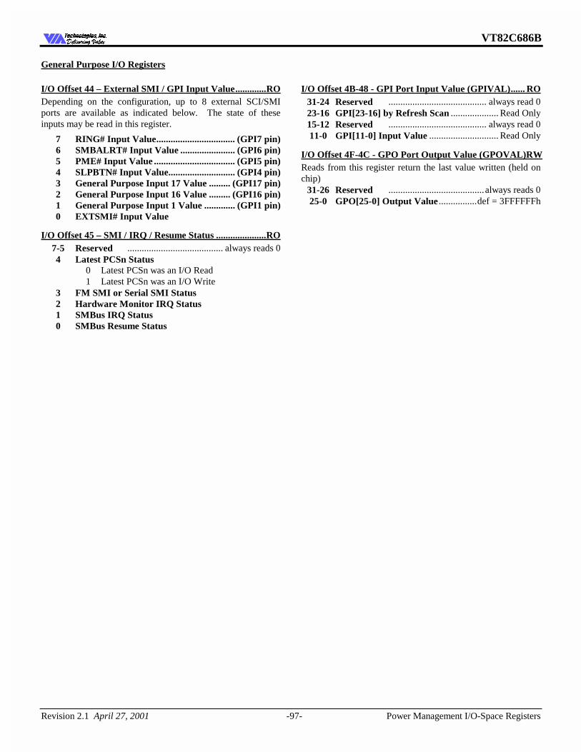
VT82C686B
Revision 2.1 April 27, 2001 -97- Power Management I/O-Space Registers
7HFKQRORJLHV ,QF'HOLYHULQJ 9DOXH'HOLYHULQJ 9DOXH
General Purpose I/O Registers
I/O Offset 44 – External SMI / GPI Input Value.............RO Depending on the configuration, up to 8 external SCI/SMI ports are available as indicated below. The state of these inputs may be read in this register.
7 RING# Input Value................................. (GPI7 pin) 6 SMBALRT# Input Value ....................... (GPI6 pin) 5 PME# Input Value .................................. (GPI5 pin) 4 SLPBTN# Input Value............................ (GPI4 pin) 3 General Purpose Input 17 Value ......... (GPI17 pin) 2 General Purpose Input 16 Value ......... (GPI16 pin) 1 General Purpose Input 1 Value ............. (GPI1 pin) 0 EXTSMI# Input Value
I/O Offset 45 – SMI / IRQ / Resume Status .....................RO 7-5 Reserved ........................................ always reads 0 4 Latest PCSn Status 0 Latest PCSn was an I/O Read 1 Latest PCSn was an I/O Write 3 FM SMI or Serial SMI Status 2 Hardware Monitor IRQ Status 1 SMBus IRQ Status 0 SMBus Resume Status
I/O Offset 4B-48 - GPI Port Input Value (GPIVAL)...... RO 31-24 Reserved ......................................... always read 0 23-16 GPI[23-16] by Refresh Scan .................... Read Only 15-12 Reserved ......................................... always read 0 11-0 GPI[11-0] Input Value ............................. Read Only
I/O Offset 4F-4C - GPO Port Output Value (GPOVAL)RW Reads from this register return the last value written (held on chip) 31-26 Reserved ........................................always reads 0 25-0 GPO[25-0] Output Value ................def = 3FFFFFFh
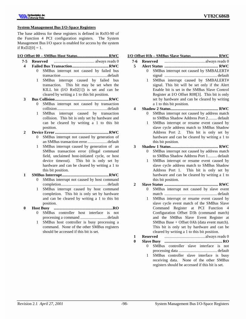
VT82C686B
Revision 2.1 April 27, 2001 -98- System Management Bus I/O-Space Registers
7HFKQRORJLHV ,QF'HOLYHULQJ 9DOXH'HOLYHULQJ 9DOXH
System Management Bus I/O-Space Registers
The base address for these registers is defined in Rx93-90 of the Function 4 PCI configuration registers. The System Management Bus I/O space is enabled for access by the system if RxD2[0] = 1.
I/O Offset 00 – SMBus Host Status...............................RWC 7-5 Reserved ........................................ always reads 0 4 Failed Bus Transaction....................................RWC 0 SMBus interrupt not caused by failed bus
transaction ..............................................default 1 SMBus interrupt caused by failed bus
transaction. This bit may be set when the KILL bit (I/O Rx02[1]) is set and can be cleared by writing a 1 to this bit position.
3 Bus Collision.....................................................RWC 0 SMBus interrupt not caused by transaction
collision..................................................default 1 SMBus interrupt caused by transaction
collision. This bit is only set by hardware and can be cleared by writing a 1 to this bit position.
2 Device Error .....................................................RWC 0 SMBus interrupt not caused by generation of
an SMBus transaction error....................default 1 SMBus interrupt caused by generation of an
SMBus transaction error (illegal command field, unclaimed host-initiated cycle, or host device timeout). This bit is only set by hardware and can be cleared by writing a 1 to this bit position.
1 SMBus Interrupt..............................................RWC 0 SMBus interrupt not caused by host command
completion..............................................default 1 SMBus interrupt caused by host command
completion. This bit is only set by hardware and can be cleared by writing a 1 to this bit position.
0 Host Busy ..........................................................RO 0 SMBus controller host interface is not
processing a command ...........................default 1 SMBus host controller is busy processing a
command. None of the other SMBus registers should be accessed if this bit is set.
I/O Offset 01h – SMBus Slave Status........................... RWC 7-6 Reserved ........................................always reads 0 5 Alert Status ..................................................... RWC 0 SMBus interrupt not caused by SMBALERT#
signal .................................................... default 1 SMBus interrupt caused by SMBALERT#
signal. This bit will be set only if the Alert Enable bit is set in the SMBus Slave Control Register at I/O Offset R08[3]. This bit is only set by hardware and can be cleared by writing a 1 to this bit position.
4 Shadow 2 Status............................................... RWC 0 SMBus interrupt not caused by address match
to SMBus Shadow Address Port 2......... default 1 SMBus interrupt or resume event caused by
slave cycle address match to SMBus Shadow Address Port 2. This bit is only set by hardware and can be cleared by writing a 1 to this bit position.
3 Shadow 1 Status............................................... RWC 0 SMBus interrupt not caused by address match
to SMBus Shadow Address Port 1......... default 1 SMBus interrupt or resume event caused by
slave cycle address match to SMBus Shadow Address Port 1. This bit is only set by hardware and can be cleared by writing a 1 to this bit position.
2 Slave Status ..................................................... RWC 0 SMBus interrupt not caused by slave event
match .................................................... default 1 SMBus interrupt or resume event caused by
slave cycle event match of the SMBus Slave Command Register at PCI Function 4 Configuration Offset D3h (command match) and the SMBus Slave Event Register at SMBus Base + Offset 0Ah (data event match). This bit is only set by hardware and can be cleared by writing a 1 to this bit position.
1 Reserved ........................................always reads 0 0 Slave Busy ......................................................... RO 0 SMBus controller slave interface is not
processing data ...................................... default 1 SMBus controller slave interface is busy
receiving data. None of the other SMBus registers should be accessed if this bit is set.
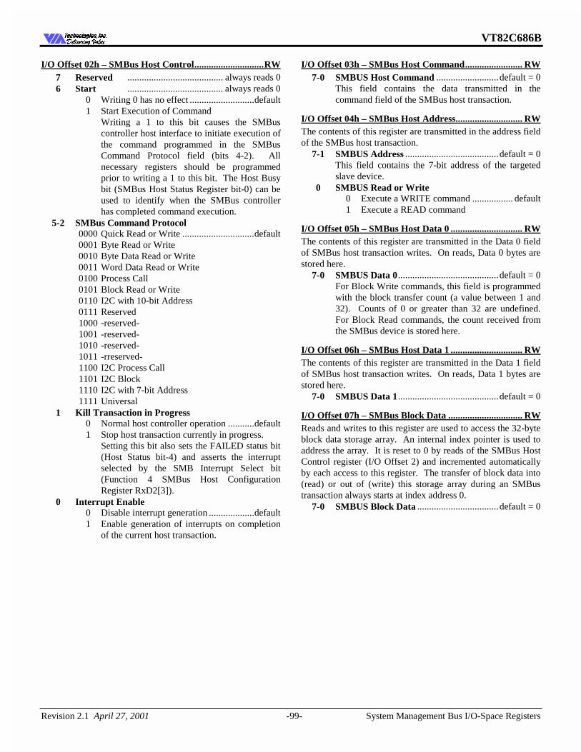
VT82C686B
Revision 2.1 April 27, 2001 -99- System Management Bus I/O-Space Registers
7HFKQRORJLHV ,QF'HOLYHULQJ 9DOXH'HOLYHULQJ 9DOXH
I/O Offset 02h – SMBus Host Control.............................RW 7 Reserved ........................................ always reads 0 6 Start ........................................ always reads 0 0 Writing 0 has no effect ...........................default 1 Start Execution of Command Writing a 1 to this bit causes the SMBus
controller host interface to initiate execution of the command programmed in the SMBus Command Protocol field (bits 4-2). All necessary registers should be programmed prior to writing a 1 to this bit. The Host Busy bit (SMBus Host Status Register bit-0) can be used to identify when the SMBus controller has completed command execution.
5-2 SMBus Command Protocol 0000 Quick Read or Write ..............................default 0001 Byte Read or Write 0010 Byte Data Read or Write 0011 Word Data Read or Write 0100 Process Call 0101 Block Read or Write 0110 I2C with 10-bit Address 0111 Reserved 1000 -reserved- 1001 -reserved- 1010 -reserved- 1011 -rreserved- 1100 I2C Process Call 1101 I2C Block 1110 I2C with 7-bit Address 1111 Universal 1 Kill Transaction in Progress 0 Normal host controller operation ...........default 1 Stop host transaction currently in progress. Setting this bit also sets the FAILED status bit
(Host Status bit-4) and asserts the interrupt selected by the SMB Interrupt Select bit (Function 4 SMBus Host Configuration Register RxD2[3]).
0 Interrupt Enable 0 Disable interrupt generation ...................default 1 Enable generation of interrupts on completion
of the current host transaction.
I/O Offset 03h – SMBus Host Command........................ RW 7-0 SMBUS Host Command ..........................default = 0 This field contains the data transmitted in the
command field of the SMBus host transaction.
I/O Offset 04h – SMBus Host Address............................ RW The contents of this register are transmitted in the address field of the SMBus host transaction. 7-1 SMBUS Address .......................................default = 0 This field contains the 7-bit address of the targeted
slave device. 0 SMBUS Read or Write 0 Execute a WRITE command ................. default 1 Execute a READ command
I/O Offset 05h – SMBus Host Data 0 .............................. RW The contents of this register are transmitted in the Data 0 field of SMBus host transaction writes. On reads, Data 0 bytes are stored here. 7-0 SMBUS Data 0..........................................default = 0 For Block Write commands, this field is programmed
with the block transfer count (a value between 1 and 32). Counts of 0 or greater than 32 are undefined. For Block Read commands, the count received from the SMBus device is stored here.
I/O Offset 06h – SMBus Host Data 1 .............................. RW The contents of this register are transmitted in the Data 1 field of SMBus host transaction writes. On reads, Data 1 bytes are stored here. 7-0 SMBUS Data 1..........................................default = 0
I/O Offset 07h – SMBus Block Data ............................... RW Reads and writes to this register are used to access the 32-byte block data storage array. An internal index pointer is used to address the array. It is reset to 0 by reads of the SMBus Host Control register (I/O Offset 2) and incremented automatically by each access to this register. The transfer of block data into (read) or out of (write) this storage array during an SMBus transaction always starts at index address 0. 7-0 SMBUS Block Data ..................................default = 0
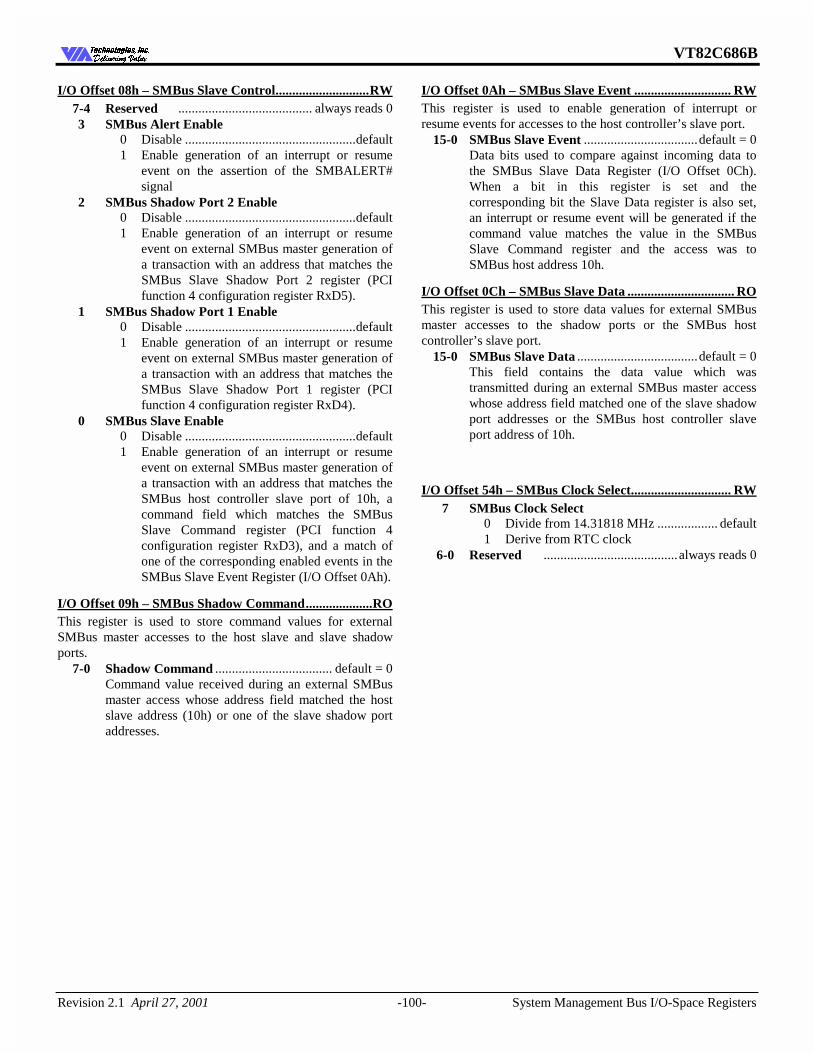
VT82C686B
Revision 2.1 April 27, 2001 -100- System Management Bus I/O-Space Registers
7HFKQRORJLHV ,QF'HOLYHULQJ 9DOXH'HOLYHULQJ 9DOXH
I/O Offset 08h – SMBus Slave Control............................RW 7-4 Reserved ........................................ always reads 0 3 SMBus Alert Enable 0 Disable ...................................................default 1 Enable generation of an interrupt or resume
event on the assertion of the SMBALERT# signal
2 SMBus Shadow Port 2 Enable 0 Disable ...................................................default 1 Enable generation of an interrupt or resume
event on external SMBus master generation of a transaction with an address that matches the SMBus Slave Shadow Port 2 register (PCI function 4 configuration register RxD5).
1 SMBus Shadow Port 1 Enable 0 Disable ...................................................default 1 Enable generation of an interrupt or resume
event on external SMBus master generation of a transaction with an address that matches the SMBus Slave Shadow Port 1 register (PCI function 4 configuration register RxD4).
0 SMBus Slave Enable 0 Disable ...................................................default 1 Enable generation of an interrupt or resume
event on external SMBus master generation of a transaction with an address that matches the SMBus host controller slave port of 10h, a command field which matches the SMBus Slave Command register (PCI function 4 configuration register RxD3), and a match of one of the corresponding enabled events in the SMBus Slave Event Register (I/O Offset 0Ah).
I/O Offset 09h – SMBus Shadow Command....................RO This register is used to store command values for external SMBus master accesses to the host slave and slave shadow ports. 7-0 Shadow Command ................................... default = 0 Command value received during an external SMBus
master access whose address field matched the host slave address (10h) or one of the slave shadow port addresses.
I/O Offset 0Ah – SMBus Slave Event ............................. RW This register is used to enable generation of interrupt or resume events for accesses to the host controller’s slave port. 15-0 SMBus Slave Event ..................................default = 0 Data bits used to compare against incoming data to
the SMBus Slave Data Register (I/O Offset 0Ch). When a bit in this register is set and the corresponding bit the Slave Data register is also set, an interrupt or resume event will be generated if the command value matches the value in the SMBus Slave Command register and the access was to SMBus host address 10h.
I/O Offset 0Ch – SMBus Slave Data ................................ RO This register is used to store data values for external SMBus master accesses to the shadow ports or the SMBus host controller’s slave port. 15-0 SMBus Slave Data ....................................default = 0 This field contains the data value which was
transmitted during an external SMBus master access whose address field matched one of the slave shadow port addresses or the SMBus host controller slave port address of 10h.
I/O Offset 54h – SMBus Clock Select.............................. RW 7 SMBus Clock Select 0 Divide from 14.31818 MHz .................. default 1 Derive from RTC clock 6-0 Reserved ........................................always reads 0
VT82C686B
Revision 2.1 April 27, 2001 -101- Hardware Monitor I/O Space Registers
7HFKQRORJLHV ,QF'HOLYHULQJ 9DOXH'HOLYHULQJ 9DOXH
Hardware Monitor I/O Space Registers
The I/O base address for access to the Hardware Monitor registers is defined in Rx71-70 of function 4 PCI configuration space. The hardware monitor I/O space is enabled for I/O access by the system if Rx74[0] = 1.
Offset 13 – Analog Data 15-8 ...........................................RW
Offset 14 – Analog Data 7-0 .............................................RW
Offset 15 – Digital Data 7-0 ..............................................RW
Offset 16 – Channel Counter............................................RW
Offset 17 – Data Valid & Channel Indicators.................RW Offset 20 – TSENS1 Temperature Reading ....................RW Temperature sensor 1 is an external sensor input on pin W13 which has 10-bit resolution. The high order 8 bits are stored here and the low order 2 bits are stored in Rx4B[7-6]. Only the high order 8 bits are used for comparison with the limit values in offsets 39 and 3A. Offset 21 – TSENS2 Temperature Reading ....................RW Temperature sensor 2 is an external sensor input on pin Y13 which has 10-bit resolution. The high order 8 bits are stored here and the low order 2 bits are stored in Rx49[5-4]. Only the high order 8 bits are used for comparison with the limit values in offsets 3D and 3E. Offset 22 – VSENS1 (Pin U13) Voltage Reading (2.0V).RW
Offset 23 – VSENS2 (Pin V13) Voltage Reading (2.5V).RW
Offset 24 – Internal Core Voltage Reading (3.3V) .........RW
Offset 25 – VSENS3 (Pin W14) Voltage Reading (5V) ..RW
Offset 26 – VSENS4 (Pin Y14) Voltage Reading (12V)..RW Offset 27 – Reserved (-12V Sense Voltage Reading) ......RW
Offset 28 – Reserved (-5V Sense Voltage Reading) ........RW
Offset 29 – FAN1 (Pin T12) Count Reading................... RW Offset 2A – FAN2 (Pin U12) Count Reading.................. RW The above two locations store the number of counts of the internal clock per fan revolution. Offset 2B – VSENS1 Voltage High Limit (CPU 2.0V)... RW
Offset 2C – VSENS1 Voltage Low Limit (CPU 2.0V) ... RW
Offset 2D – VSENS2 Voltage High Limit (NB 2.5V) ..... RW
Offset 2E – VSENS2 Voltage Low Limit (NB 2.5V) ...... RW
Offset 2F – Internal Core Voltage High Limit (3.3V).... RW
Offset 30 – Internal Core Voltage Low Limit (3.3V)..... RW
Offset 31 – VSENS3 Voltage High Limit (5V)................ RW
Offset 32 – VSENS3 Voltage Low Limit (5V) ................ RW
Offset 33 – VSENS4 Voltage High Limit (12V).............. RW
Offset 34 – VSENS4 Voltage Low Limit (12V) .............. RW Offset 35 – Reserved (-12V Sense High Limit) ............... RW
Offset 36 – Reserved (-12V Sense Low Limit)................ RW
Offset 37 – Reserved (-5V Sense High Limit) ................. RW
Offset 38 – Reserved (-5V Sense Low Limit).................. RW Offset 39 – TSENS1 Hot Temperature High Limit........ RW
Offset 3A – TSENS1Hot Temp Hysteresis Lo Limit...... RW Offset 3B – FAN1 Fan Count Limit ................................ RW
Offset 3C – FAN2 Fan Count Limit ................................ RW The above two locations store the number of counts of the internal clock per fan revolution for the low limit of the fan speed. Offset 3D – TSENS2 Hot Temperature High Limit....... RW
Offset 3E – TSENS2 Hot Temp Hysteresis Lo Limit ..... RW Offset 3F – Stepping ID Number..................................... RW
Note: For high limits, comparisons are “greater than” comparisons. For low limits, comparisons are “less than or equal” comparisons.
One consequence of the above is that if high limits are set to all ones (FFh or 11111111b), interrupts are disabled for high limits (i.e., interrupts will only be generated for cases when voltages are equal to or below the low limits).
VT82C686B
Revision 2.1 April 27, 2001 -102- Hardware Monitor I/O Space Registers
7HFKQRORJLHV ,QF'HOLYHULQJ 9DOXH'HOLYHULQJ 9DOXH
Offset 40 –Hardware Monitor Configuration ................RW 7 Initialization 0 Normal operation ...................................default 1 Restore power-up default values to this
register, the interrupt status and mask registers, the FAN/RST#/OS# register, and the OS# Configuration / Temperature Resolution register. This bit automatically clears itself since the power-on default is 0.
6 Chassis Intrusion Reset 0 Normal operation ...................................default 1 Reset the Chassis Intrusion pin 5-4 Reserved (R/W) ........................................ default = 0 3 Hardware Monitor Interrupt Clear 0 Normal operation 1 Clear the hardware monitor interrupt output
(does not effect the contents of the interrupt status register). Normally set during interrupt service ....................................................default
2 Reserved ........................................ always reads 0 1 Hardware Monitor Interrupt Enable 0 Disable hardware monitor interrupt output.. def 1 Enable hardware monitor interrupt output 0 Start 0 Place hardware monitor in standby mode.... def 1 Enable startup of hardware monitor logic. At startup, limit checking functions and
scanning begins. All high and low limits should be set prior to turning on this bit. Note: the hardware monitor interrupt output will not be cleared if the user writes a zero to this bit after an interrupt has occurred (the hardware monitor interrupt clear bit must be used for this purpose).
VT82C686B
Revision 2.1 April 27, 2001 -103- Hardware Monitor I/O Space Registers
7HFKQRORJLHV ,QF'HOLYHULQJ 9DOXH'HOLYHULQJ 9DOXH
Offset 41 –Hardware Monitor Interrupt Status 1...........RO 7 Fan 2 Error 0 No error ..................................................default 1 Fan 2 count limit exceeded 6 Fan 1 Error 0 No error ..................................................default 1 Fan 1 count limit exceeded 5 Reserved ........................................ always reads 0 4 TSENS1 Temperature Error 0 No error ..................................................default 1 High or low hot temperature limit exceeded.
The interrupt mode is determined by Temperature Resolution register Rx4B[1-0].
3 VSENS3 Voltage Error (5V) 0 No error ..................................................default 1 High or low limit exceeded 2 Internal Core VCC Voltage Error (3.3V) 0 No error ..................................................default 1 High or low limit exceeded 1 VSENS2 Voltage Error (2.5V NB Core Voltage) 0 No error ..................................................default 1 High or low limit exceeded 0 VSENS1 Voltage Error (2.0V CPU Core Voltage) 0 No error ..................................................default 1 High or low limit exceeded
Offset 42 –Hardware Monitor Interrupt Status 2...........RO 7-5 Reserved ........................................ always reads 0 4 Chassis Error 0 No error ..................................................default 1 Chassis Intrusion has gone high 3 TSENS2 Temperature Error 0 No error ..................................................default 1 High or low hot temperature limit exceeded.
Interrupt mode is determined by Rx4B[3-2]. 2-1 Reserved ........................................ always reads 0 0 VSENS4 Voltage Error (12V) 0 No error ..................................................default 1 High or low limit exceeded Note: When either status register is read, status conditions in that register are reset. In the case of voltage priority indications, if two or more voltages were out of limits, then another indication would automatically be generated if it was not handled during interrupt service. Errant voltages may be disabled in the control register until the operator has time to clear the errant condition or set the limit higher or lower.
Offset 43 –Hardware Monitor Interrupt Mask 1 .......... RW 7 Fan 2 Count Error Mask 0 Enable interrupt on error status bit set ......... def 1 Disable interrupt on error status bit set 6 Fan 1 Count Error Mask 0 Enable interrupt on error status bit set ......... def 1 Disable interrupt on error status bit set 5 TSENS1 Thermal Alarm Control Mask 0 Enable TSENS1 over-temp condition to
control the thermal alarm (function 4 Rx40[7] automatic CPU clock throttling must be set )def
1 Disable 4 TSENS1 Temperature Error Mask 0 Enable interrupt on error status bit set ......... def 1 Disable interrupt on error status bit set 3 VSENS3 Voltage Error Mask (5V) 0 Enable interrupt on error status bit set ......... def 1 Disable interrupt on error status bit set 2 Internal Core VCC Voltage Error Mask (3.3V) 0 Enable interrupt on error status bit set ......... def 1 Disable interrupt on error status bit set 1 VSENS2 Voltage Error Mask (2.5V NB Core) 0 Enable interrupt on error status bit set ......... def 1 Disable interrupt on error status bit set 0 VSENS1 Voltage Error Mask (2.0V CPU Core) 0 Enable interrupt on error status bit set ......... def 1 Disable interrupt on error status bit set
Offset 44 –Hardware Monitor Interrupt Mask 2 .......... RW 7-6 Reserved ........................................always reads 0 5 TSENS2 Thermal Alarm Control Mask 0 Enable TSENS2 over-temp condition to
control the thermal alarm (function 4 Rx40[7] automatic CPU clock throttling must be set)def
1 Disable 4 Chassis Error Mask 0 Enable interrupt on error status bit set ......... def 1 Disable interrupt on error status bit set 3 TSENS2 Temperature Error Mask 0 Enable interrupt on error status bit set ......... def 1 Disable interrupt on error status bit set 2-1 Reserved ........................................always reads 0 0 VSENS4 Voltage Error Mask (12V) 0 Enable interrupt on error status bit set ......... def 1 Disable interrupt on error status bit set
VT82C686B
Revision 2.1 April 27, 2001 -104- Hardware Monitor I/O Space Registers
7HFKQRORJLHV ,QF'HOLYHULQJ 9DOXH'HOLYHULQJ 9DOXH
Offset 47 –Hardware Monitor Fan Configuration.........RW 7-6 Fan 2 RPM Control 00 Divide by 1 01 Divide by 2 ............................................default 10 Divide by 4 11 Divide by 8 5-4 Fan 1 RPM Control 00 Divide by 1 01 Divide by 2 ............................................default 10 Divide by 4 11 Divide by 8 3-0 Reserved ........................................ always reads 0
Offset 49 –Hardware Monitor Temp Low Order ValueRW 7-6 Reserved ........................................ always reads 0 5-4 TSENS2 Value Low-Order Bits Upper 8 bits are stored in offset 21h 3 Over Temperature Active Low for PMU to
Control Stop Clock 0 Disable ...................................................default 1 Enable 2 Chassis Active Low Output 20 msec 0 Disable ...................................................default 1 Enable 1 Interrupt Active High Output 0 Disable ...................................................default 1 Enable 0 Reserved ........................................ always reads 0
Offset 4B –Temperature Interrupt Configuration ........ RW 7-6 TSENS1 Value Low-Order Bits ..................def = 00 Upper 8 bits are stored in offset 20h 5-4 Reserved ........................................always reads 0 3-2 TSENS2 Hot Temp Interrupt Mode ...........def = 01 1-0 TSENS1 Hot Temp Interrupt Mode ...........def = 01 The following applies to each of the above 3 fields 00 Default Interrupt Mode. An interrupt occurs if
the temperature goes above the hot limit. The interrupt will be cleared once the status register is read, but will be generated again when the next conversion is completed. Interrupts will continue to be generated until the temperature goes below the hysteresis limit.
01 One-Time Interrupt Mode. An interrupt is generated if the temperrature goes above the hot limit. The interrupt will be cleared when the status register is read. Another interrupt will not be generated until the temperature first drops below the hysteresis limit............. default
10 Comparator mode. An interrupt occurs if the temperature goes above the hot limit. This interrupt remains active until the temperature goes below the hot limit (i.e., no hysteresis).
11 Default Interrupt Mode (same as 00)
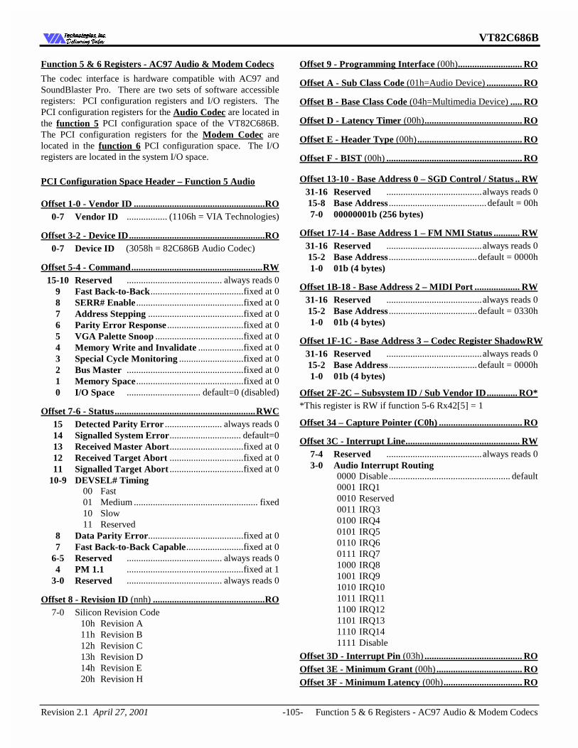
VT82C686B
Revision 2.1 April 27, 2001 -105- Function 5 & 6 Registers - AC97 Audio & Modem Codecs
7HFKQRORJLHV ,QF'HOLYHULQJ 9DOXH'HOLYHULQJ 9DOXH
Function 5 & 6 Registers - AC97 Audio & Modem Codecs
The codec interface is hardware compatible with AC97 and SoundBlaster Pro. There are two sets of software accessible registers: PCI configuration registers and I/O registers. The PCI configuration registers for the Audio Codec are located in the function 5 PCI configuration space of the VT82C686B. The PCI configuration registers for the Modem Codec are located in the function 6 PCI configuration space. The I/O registers are located in the system I/O space.
PCI Configuration Space Header – Function 5 Audio
Offset 1-0 - Vendor ID .......................................................RO 0-7 Vendor ID ................. (1106h = VIA Technologies)
Offset 3-2 - Device ID.........................................................RO 0-7 Device ID (3058h = 82C686B Audio Codec)
Offset 5-4 - Command.......................................................RW 15-10 Reserved ........................................ always reads 0 9 Fast Back-to-Back.......................................fixed at 0 8 SERR# Enable .............................................fixed at 0 7 Address Stepping ........................................fixed at 0 6 Parity Error Response ................................fixed at 0 5 VGA Palette Snoop .....................................fixed at 0 4 Memory Write and Invalidate ...................fixed at 0 3 Special Cycle Monitoring ...........................fixed at 0 2 Bus Master .................................................fixed at 0 1 Memory Space.............................................fixed at 0 0 I/O Space ............................... default=0 (disabled)
Offset 7-6 - Status...........................................................RWC 15 Detected Parity Error ........................ always reads 0 14 Signalled System Error.............................. default=0 13 Received Master Abort...............................fixed at 0 12 Received Target Abort ...............................fixed at 0 11 Signalled Target Abort ...............................fixed at 0 10-9 DEVSEL# Timing 00 Fast 01 Medium .................................................... fixed 10 Slow 11 Reserved 8 Data Parity Error........................................fixed at 0 7 Fast Back-to-Back Capable........................fixed at 0 6-5 Reserved ........................................ always reads 0 4 PM 1.1 .................................................fixed at 1 3-0 Reserved ........................................ always reads 0
Offset 8 - Revision ID (nnh) ...............................................RO 7-0 Silicon Revision Code 10h Revision A 11h Revision B 12h Revision C 13h Revision D 14h Revision E 20h Revision H
Offset 9 - Programming Interface (00h)........................... RO
Offset A - Sub Class Code (01h=Audio Device) ............... RO
Offset B - Base Class Code (04h=Multimedia Device) ..... RO
Offset D - Latency Timer (00h)......................................... RO
Offset E - Header Type (00h) ............................................ RO
Offset F - BIST (00h) ......................................................... RO
Offset 13-10 - Base Address 0 – SGD Control / Status .. RW 31-16 Reserved ........................................always reads 0 15-8 Base Address .........................................default = 00h 7-0 00000001b (256 bytes)
Offset 17-14 - Base Address 1 – FM NMI Status ........... RW 31-16 Reserved ........................................always reads 0 15-2 Base Address .....................................default = 0000h 1-0 01b (4 bytes)
Offset 1B-18 - Base Address 2 – MIDI Port ................... RW 31-16 Reserved ........................................always reads 0 15-2 Base Address .....................................default = 0330h 1-0 01b (4 bytes)
Offset 1F-1C - Base Address 3 – Codec Register ShadowRW 31-16 Reserved ........................................always reads 0 15-2 Base Address .....................................default = 0000h 1-0 01b (4 bytes)
Offset 2F-2C – Subsystem ID / Sub Vendor ID............. RO* *This register is RW if function 5-6 Rx42[5] = 1
Offset 34 – Capture Pointer (C0h) ................................... RO
Offset 3C - Interrupt Line................................................ RW 7-4 Reserved ........................................always reads 0 3-0 Audio Interrupt Routing 0000 Disable................................................... default 0001 IRQ1 0010 Reserved 0011 IRQ3 0100 IRQ4 0101 IRQ5 0110 IRQ6 0111 IRQ7 1000 IRQ8 1001 IRQ9 1010 IRQ10 1011 IRQ11 1100 IRQ12 1101 IRQ13 1110 IRQ14 1111 Disable
Offset 3D - Interrupt Pin (03h) ......................................... RO Offset 3E - Minimum Grant (00h) .................................... RO Offset 3F - Minimum Latency (00h)................................. RO
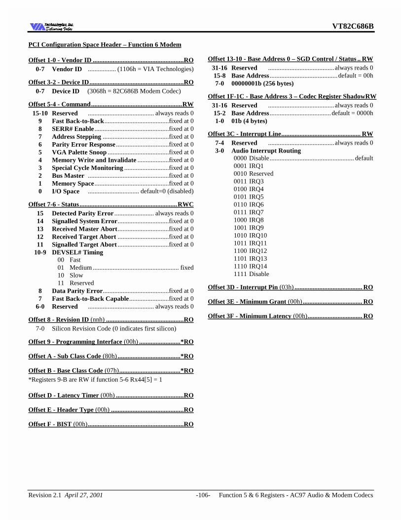
VT82C686B
Revision 2.1 April 27, 2001 -106- Function 5 & 6 Registers - AC97 Audio & Modem Codecs
7HFKQRORJLHV ,QF'HOLYHULQJ 9DOXH'HOLYHULQJ 9DOXH
PCI Configuration Space Header – Function 6 Modem
Offset 1-0 - Vendor ID .......................................................RO 0-7 Vendor ID ................. (1106h = VIA Technologies)
Offset 3-2 - Device ID.........................................................RO 0-7 Device ID (3068h = 82C686B Modem Codec)
Offset 5-4 - Command.......................................................RW 15-10 Reserved ........................................ always reads 0 9 Fast Back-to-Back.......................................fixed at 0 8 SERR# Enable .............................................fixed at 0 7 Address Stepping ........................................fixed at 0 6 Parity Error Response ................................fixed at 0 5 VGA Palette Snoop .....................................fixed at 0 4 Memory Write and Invalidate ...................fixed at 0 3 Special Cycle Monitoring ...........................fixed at 0 2 Bus Master .................................................fixed at 0 1 Memory Space.............................................fixed at 0 0 I/O Space ............................... default=0 (disabled)
Offset 7-6 - Status...........................................................RWC 15 Detected Parity Error ........................ always reads 0 14 Signalled System Error...............................fixed at 0 13 Received Master Abort...............................fixed at 0 12 Received Target Abort ...............................fixed at 0 11 Signalled Target Abort ...............................fixed at 0 10-9 DEVSEL# Timing 00 Fast 01 Medium .................................................... fixed 10 Slow 11 Reserved 8 Data Parity Error........................................fixed at 0 7 Fast Back-to-Back Capable........................fixed at 0 6-0 Reserved ........................................ always reads 0
Offset 8 - Revision ID (nnh) ...............................................RO 7-0 Silicon Revision Code (0 indicates first silicon)
Offset 9 - Programming Interface (00h) .........................*RO
Offset A - Sub Class Code (80h) ......................................*RO
Offset B - Base Class Code (07h).....................................*RO *Registers 9-B are RW if function 5-6 Rx44[5] = 1
Offset D - Latency Timer (00h) .........................................RO
Offset E - Header Type (00h) ............................................RO
Offset F - BIST (00h)..........................................................RO
Offset 13-10 - Base Address 0 – SGD Control / Status .. RW 31-16 Reserved ........................................always reads 0 15-8 Base Address .........................................default = 00h 7-0 00000001b (256 bytes)
Offset 1F-1C - Base Address 3 – Codec Register ShadowRW 31-16 Reserved ........................................always reads 0 15-2 Base Address .....................................default = 0000h 1-0 01b (4 bytes)
Offset 3C - Interrupt Line................................................ RW 7-4 Reserved ........................................always reads 0 3-0 Audio Interrupt Routing 0000 Disable................................................... default 0001 IRQ1 0010 Reserved 0011 IRQ3 0100 IRQ4 0101 IRQ5 0110 IRQ6 0111 IRQ7 1000 IRQ8 1001 IRQ9 1010 IRQ10 1011 IRQ11 1100 IRQ12 1101 IRQ13 1110 IRQ14 1111 Disable
Offset 3D - Interrupt Pin (03h) ......................................... RO
Offset 3E - Minimum Grant (00h) .................................... RO
Offset 3F - Minimum Latency (00h)................................. RO
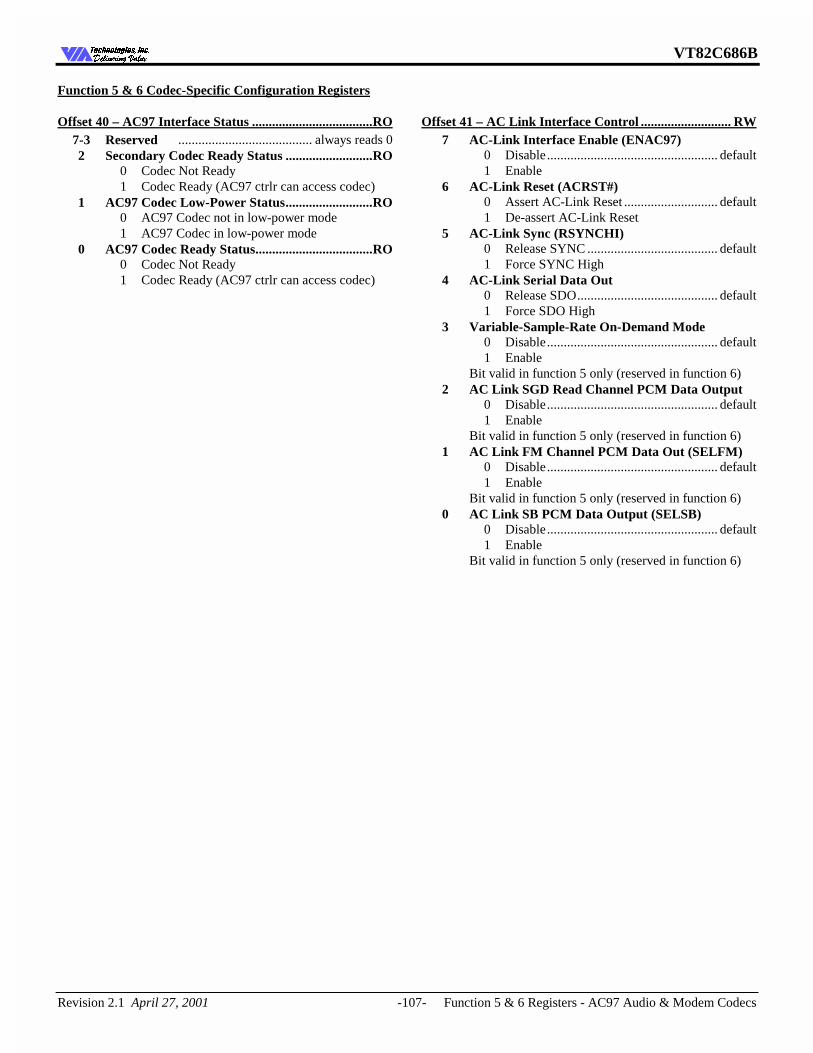
VT82C686B
Revision 2.1 April 27, 2001 -107- Function 5 & 6 Registers - AC97 Audio & Modem Codecs
7HFKQRORJLHV ,QF'HOLYHULQJ 9DOXH'HOLYHULQJ 9DOXH
Function 5 & 6 Codec-Specific Configuration Registers
Offset 40 – AC97 Interface Status ....................................RO 7-3 Reserved ........................................ always reads 0 2 Secondary Codec Ready Status ..........................RO 0 Codec Not Ready 1 Codec Ready (AC97 ctrlr can access codec) 1 AC97 Codec Low-Power Status..........................RO 0 AC97 Codec not in low-power mode 1 AC97 Codec in low-power mode 0 AC97 Codec Ready Status...................................RO 0 Codec Not Ready 1 Codec Ready (AC97 ctrlr can access codec)
Offset 41 – AC Link Interface Control ........................... RW 7 AC-Link Interface Enable (ENAC97) 0 Disable................................................... default 1 Enable 6 AC-Link Reset (ACRST#) 0 Assert AC-Link Reset ............................ default 1 De-assert AC-Link Reset 5 AC-Link Sync (RSYNCHI) 0 Release SYNC ....................................... default 1 Force SYNC High 4 AC-Link Serial Data Out 0 Release SDO.......................................... default 1 Force SDO High 3 Variable-Sample-Rate On-Demand Mode 0 Disable................................................... default 1 Enable Bit valid in function 5 only (reserved in function 6) 2 AC Link SGD Read Channel PCM Data Output 0 Disable................................................... default 1 Enable Bit valid in function 5 only (reserved in function 6) 1 AC Link FM Channel PCM Data Out (SELFM) 0 Disable................................................... default 1 Enable Bit valid in function 5 only (reserved in function 6) 0 AC Link SB PCM Data Output (SELSB) 0 Disable................................................... default 1 Enable Bit valid in function 5 only (reserved in function 6)
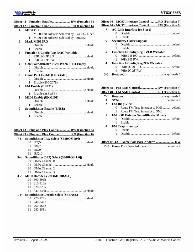
VT82C686B
Revision 2.1 April 27, 2001 -108- Function 5 & 6 Registers - AC97 Audio & Modem Codecs
7HFKQRORJLHV ,QF'HOLYHULQJ 9DOXH'HOLYHULQJ 9DOXH
Offset 42 – Function Enable .......................RW (Function 5) Offset 42 – Function Enable ........................RO (Function 6) 7 MIDI PnP 0 MIDI Port Address Selected by Rx43[3-2] . def 1 MIDI Port Address Selected by IOBase2 6 Mask MIDI IRQ 0 Disable ...................................................default 1 Enable 5 Function 5 Config Reg Rx2C Writable 0 F5Rx2C-2F RO ......................................default 1 F5Rx2C-2F RW 4 Gate SoundBlaster PCM When FIFO Empty 0 Disable ...................................................default 1 Enable 3 Game Port Enable (ENGAME) 0 Disable ...................................................default 1 Enable (200-207h) 2 FM Enable (ENFM) 0 Disable ...................................................default 1 Enable (388-38B) 1 MIDI Enable (ENMIDI) 0 Disable ...................................................default 1 Enable 0 SoundBlaster Enable (ENSB) 0 Disable ...................................................default 1 Enable
Offset 43 – Plug and Play Control .............RW (Function 5) Offset 43 – Plug and Play Control ..............RO (Function 6) 7-6 SoundBlaster IRQ Select (SBIRQS[1:0]) 00 IRQ5 .....................................................default 01 IRQ7 10 IRQ9 11 IRQ10 5-4 SoundBlaster DRQ Select (SBDRQS[1:0]) 00 DMA Channel 0 01 DMA Channel 1 .....................................default 10 DMA Channel 2 11 DMA Channel 3 3-2 MIDI Decode Select (MIDIBASE) 00 300-303h 01 310-313h 10 320-323h 11 330-333h ................................................default 1-0 SoundBlaster Decode Select (SBBASE) 00 220-22Fh ................................................default 01 240-24Fh 10 260-26Fh 11 280-28Fh
Offset 44 – MC97 Interface Control .......... RO (Function 5) Offset 44 – MC97 Interface Control ......... RW (Function 6) 7 AC-Link Interface for Slot-5 0 Disable................................................... default 1 Enable 6 Secondary Codec Support 0 Disable................................................... default 1 Enable 5 Function 6 Config Reg Rx9-B Writable 0 F6Rx9-B RO.......................................... default 1 F6Rx9-B RW 4 Function 6 Config Reg 2Ch Writable 0 F6Rx2C-2F RO...................................... default 1 F6Rx2C-2F RW 3-0 Reserved ........................................always reads 0
Offset 48 – FM NMI Control ..................... RW (Function 5) Offset 48 – FM NMI Control ...................... RO (Function 6) 7-4 Reserved ........................................always reads 0 3 SYNC ..............................................default = 0 2 FM IRQ Select 0 Route FM Trap interrupt to NMI........... default 1 Route FM Trap interrupt to SMI 1 FM SGD Data for SoundBlaster Mixing 0 Disable................................................... default 1 Enable 0 FM Trap Interrupt 0 Enable 1 Disable .................................................. default Offset 4B-4A – Game Port Base Address ....................... RW 15-0 Game Port Base Address .........................default = 0
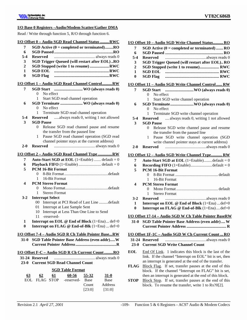
VT82C686B
Revision 2.1 April 27, 2001 -109- Function 5 & 6 Registers - AC97 Audio & Modem Codecs
7HFKQRORJLHV ,QF'HOLYHULQJ 9DOXH'HOLYHULQJ 9DOXH
I/O Base 0 Registers –Audio/Modem Scatter/Gather DMA
Read / Write through function 5, R/O through function 6.
I/O Offset 0 – Audio SGD Read Channel Status .........RWC 7 SGD Active (0 = completed or terminated)........RO 6 SGD Paused ..........................................................RO 5-4 Reserved ........................................ always reads 0 3 SGD Trigger Queued (will restart after EOL) ..RO 2 SGD Stopped (write 1 to resume) ...................RWC 1 SGD EOL ......................................................RWC 0 SGD Flag ......................................................RWC
I/O Offset 1 – Audio SGD Read Channel Control..........RW 7 SGD Start ............................ WO (always reads 0) 0 No effect 1 Start SGD read channel operation 6 SGD Terminate ...................... WO (always reads 0) 0 No effect 1 Terminate SGD read channel operation 5-4 Reserved .....always reads 0, writing 1 not allowed 3 SGD Pause 0 Release SGD read channel pause and resume
the transfer from the paused line 1 Pause SGD read channel operation (SGD read
channel pointer stays at the current address) 2-0 Reserved ........................................ always reads 0
I/O Offset 2 – Audio SGD Read Channel Type ..............RW 7 Auto-Start SGD at EOL (1=Enable) ....... default = 0 6 Playback FIFO (1=Enable) ...................... default = 0 5 PCM 16-Bit Format 0 8-Bit Format ...........................................default 1 16-Bit Format 4 PCM Stereo Format 0 Mono Format..........................................default 1 Stereo Format 3-2 Interrupt Select 00 Interrupt at PCI Read of Last Line .........default 01 Interrupt at Last Sample Sent 10 Interrupt at Less Than One Line to Send 11 -reserved- 1 Interrupt on EOL @ End of Block (1=Ena) ... def=0 0 Interrupt on FLAG @ End-of-Blk (1=Ena) ... def=0
I/O Offset 7-4 – Audio SGD R Ch Table Pointer Base...RW 31-0 SGD Table Pointer Base Address (even addr).....W Current Pointer Address ........................................R
I/O Offset F-C – Audio SGD R Ch Current Count .........RO 31-24 Reserved ........................................ always reads 0 23-0 Current SGD Read Channel Count
SGD Table Format 63 62 61 60-56 55-32 31-0 EOL FLAG STOP -reserved- Base Base Count Address [23:0] [31:0]
I/O Offset 10 – Audio SGD Write Channel Status.......... RO 7 SGD Active (0 = completed or terminated) ....... RO 6 SGD Paused ......................................................... RO 5-4 Reserved ........................................always reads 0 3 SGD Trigger Queued (will restart after EOL).. RO 2 SGD Stopped (write 1 to resume)................... RWC 1 SGD EOL ..................................................... RWC 0 SGD Flag ..................................................... RWC
I/O Offset 11 – Audio SGD Write Channel Control ...... RW 7 SGD Start ............................WO (always reads 0) 0 No effect 1 Start SGD write channel operation 6 SGD Terminate.......................WO (always reads 0) 0 No effect 1 Terminate SGD write channel operation 5-4 Reserved .... always reads 0, writing 1 not allowed 3 SGD Pause 0 Release SGD write channel pause and resume
the transfer from the paused line 1 Pause SGD write channel operation (SGD
write channel pointer stays at current address) 2-0 Reserved ........................................always reads 0
I/O Offset 12 – Audio SGD Write Channel Type........... RW 7 Auto-Start SGD at EOL (1=Enable)........default = 0 6 Recording FIFO (1=Enable).....................default = 0 5 PCM 16-Bit Format 0 8-Bit Format .......................................... default 1 16-Bit Format 4 PCM Stereo Format 0 Mono Format ......................................... default 1 Stereo Format 3-2 Reserved ........................................always reads 0 1 Interrupt on EOL @ End of Block (1=Ena) ...def=0 0 Interrupt on FLAG @ End-of-Blk (1=Ena)....def=0
I/O Offset 17-14 – Audio SGD W Ch Table Pointer BaseRW 31-0 SGD Table Pointer Base Address (even addr) .... W Current Pointer Address ....................................... R
I/O Offset 1F-1C – Audio SGD W Ch Current Count ... RO 31-24 Reserved ........................................always reads 0 23-0 Current SGD Write Channel Count
EOL End Of Link. 1 indicates this block is the last of the link. If the channel “Interrupt on EOL” bit is set, then an interrupt is generated at the end of the transfer.
FLAG Block Flag. If set, transfer pauses at the end of this block. If the channel “Interrupt on FLAG” bit is set, then an interrupt is generated at the end of this block.
STOP Block Stop. If set, transfer pauses at the end of this block. To resume the transfer, write 1 to Rx?0[2].
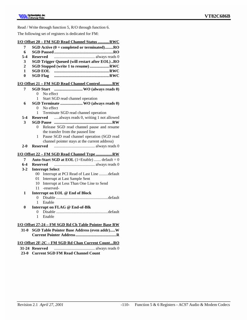
VT82C686B
Revision 2.1 April 27, 2001 -110- Function 5 & 6 Registers - AC97 Audio & Modem Codecs
7HFKQRORJLHV ,QF'HOLYHULQJ 9DOXH'HOLYHULQJ 9DOXH
Read / Write through function 5, R/O through function 6.
The following set of registers is dedicated for FM:
I/O Offset 20 – FM SGD Read Channel Status ...........RWC 7 SGD Active (0 = completed or terminated)........RO 6 SGD Paused ..........................................................RO 5-4 Reserved ........................................ always reads 0 3 SGD Trigger Queued (will restart after EOL) ..RO 2 SGD Stopped (write 1 to resume) ...................RWC 1 SGD EOL ......................................................RWC 0 SGD Flag ......................................................RWC
I/O Offset 21 – FM SGD Read Channel Control............RW 7 SGD Start ............................ WO (always reads 0) 0 No effect 1 Start SGD read channel operation 6 SGD Terminate ...................... WO (always reads 0) 0 No effect 1 Terminate SGD read channel operation 5-4 Reserved .....always reads 0, writing 1 not allowed 3 SGD Pause .........................................................RW 0 Release SGD read channel pause and resume
the transfer from the paused line 1 Pause SGD read channel operation (SGD read
channel pointer stays at the current address) 2-0 Reserved ........................................ always reads 0
I/O Offset 22 – FM SGD Read Channel Type ................RW 7 Auto-Start SGD at EOL (1=Enable) ....... default = 0 6-4 Reserved ........................................ always reads 0 3-2 Interrupt Select 00 Interrupt at PCI Read of Last Line .........default 01 Interrupt at Last Sample Sent 10 Interrupt at Less Than One Line to Send 11 -reserved- 1 Interrupt on EOL @ End of Block 0 Disable ...................................................default 1 Enable 0 Interrupt on FLAG @ End-of-Blk 0 Disable ...................................................default 1 Enable
I/O Offset 27-24 – FM SGD Rd Ch Table Pointer Base RW 31-0 SGD Table Pointer Base Address (even addr).....W Current Pointer Address ........................................R
I/O Offset 2F-2C – FM SGD Rd Chan Current Count...RO 31-24 Reserved ........................................ always reads 0 23-0 Current SGD FM Read Channel Count
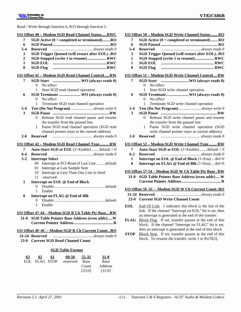
VT82C686B
Revision 2.1 April 27, 2001 -111- Function 5 & 6 Registers - AC97 Audio & Modem Codecs
7HFKQRORJLHV ,QF'HOLYHULQJ 9DOXH'HOLYHULQJ 9DOXH
Read / Write through function 6, R/O through function 5.
I/O Offset 40 – Modem SGD Read Channel Status.....RWC 7 SGD Active (0 = completed or terminated)........RO 6 SGD Paused ..........................................................RO 5-4 Reserved ........................................ always reads 0 3 SGD Trigger Queued (will restart after EOL) ..RO 2 SGD Stopped (write 1 to resume) ...................RWC 1 SGD EOL ......................................................RWC 0 SGD Flag ......................................................RWC
I/O Offset 41 – Modem SGD Read Channel Control .....RW 7 SGD Start ............................ WO (always reads 0) 0 No effect 1 Start SGD read channel operation 6 SGD Terminate ...................... WO (always reads 0) 0 No effect 1 Terminate SGD read channel operation 5-4 Test (Do Not Program) .......................always write 0 3 SGD Pause .........................................................RW 0 Release SGD read channel pause and resume
the transfer from the paused line 1 Pause SGD read channel operation (SGD read
channel pointer stays at the current address) 2-0 Reserved ........................................ always reads 0
I/O Offset 42 – Modem SGD Read Channel Type..........RW 7 Auto-Start SGD at EOL (1=Enable) ....... default = 0 6-4 Reserved ........................................ always reads 0 3-2 Interrupt Select 00 Interrupt at PCI Read of Last Line .........default 01 Interrupt at Last Sample Sent 10 Interrupt at Less Than One Line to Send 11 -reserved- 1 Interrupt on EOL @ End of Block 0 Disable ...................................................default 1 Enable 0 Interrupt on FLAG @ End-of-Blk 0 Disable ...................................................default 1 Enable
I/O Offset 47-44 – Modem SGD R Ch Table Ptr Base ...RW 31-0 SGD Table Pointer Base Address (even addr).....W Current Pointer Address ........................................R
I/O Offset 4F-4C – Modem SGD R Ch Current Count ..RO 31-24 Reserved ........................................ always reads 0 23-0 Current SGD Read Channel Count
SGD Table Format
63 62 61 60-56 55-32 31-0 EOL FLAG STOP -reserved- Base Base Count Address [23:0] [31:0]
I/O Offset 50 – Modem SGD Write Channel Status ....... RO 7 SGD Active (0 = completed or terminated) ....... RO 6 SGD Paused ......................................................... RO 5-4 Reserved ........................................always reads 0 3 SGD Trigger Queued (will restart after EOL).. RO 2 SGD Stopped (write 1 to resume)................... RWC 1 SGD EOL ..................................................... RWC 0 SGD Flag ..................................................... RWC
I/O Offset 51 – Modem SGD Write Channel Control ... RW 7 SGD Start ............................WO (always reads 0) 0 No effect 1 Start SGD write channel operation 6 SGD Terminate.......................WO (always reads 0) 0 No effect 1 Terminate SGD write channel operation 5-4 Test (Do Not Program)....................... always write 0 3 SGD Pause ........................................................ RW 0 Release SGD write channel pause and resume
the transfer from the paused line 1 Pause SGD write channel operation (SGD
write channel pointer stays at current address) 2-0 Reserved ........................................always reads 0
I/O Offset 52 – Modem SGD Write Channel Type ........ RW 7 Auto-Start SGD at EOL (1=Enable)........default = 0 6-2 Reserved ........................................always reads 0 1 Interrupt on EOL @ End of Block (1=Ena) ...def=0 0 Interrupt on FLAG @ End-of-Blk (1=Ena)....def=0
I/O Offset 57-54 – Modem SGD W Ch Table Ptr Base . RW 31-0 SGD Table Pointer Base Address (even addr) .... W Current Pointer Address ....................................... R
I/O Offset 5F-5C – Modem SGD W Ch Current Count. RO 31-24 Reserved ........................................always reads 0 23-0 Current SGD Write Channel Count
EOL End Of Link. 1 indicates this block is the last of the link. If the channel “Interrupt on EOL” bit is set, then an interrupt is generated at the end of the transfer.
FLAG Block Flag. If set, transfer pauses at the end of this block. If the channel “Interrupt on FLAG” bit is set, then an interrupt is generated at the end of this block.
STOP Block Stop. If set, transfer pauses at the end of this block. To resume the transfer, write 1 to Rx?0[2].
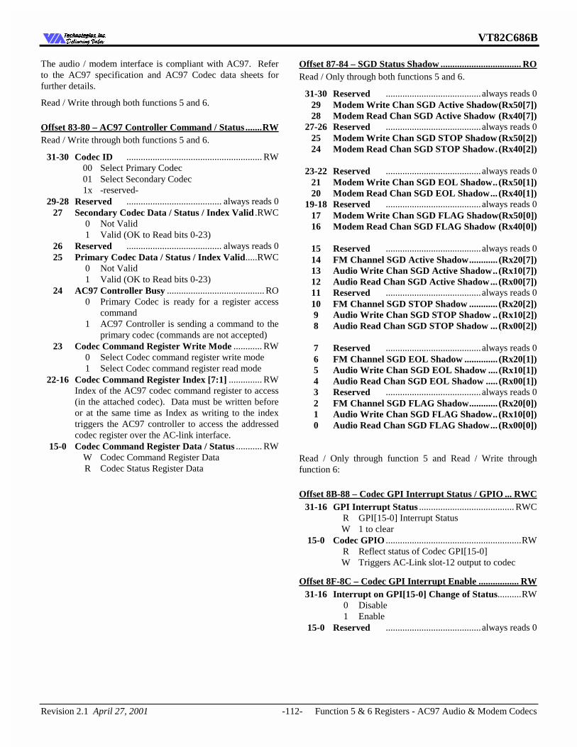
VT82C686B
Revision 2.1 April 27, 2001 -112- Function 5 & 6 Registers - AC97 Audio & Modem Codecs
7HFKQRORJLHV ,QF'HOLYHULQJ 9DOXH'HOLYHULQJ 9DOXH
The audio / modem interface is compliant with AC97. Refer to the AC97 specification and AC97 Codec data sheets for further details.
Read / Write through both functions 5 and 6.
Offset 83-80 – AC97 Controller Command / Status .......RW Read / Write through both functions 5 and 6.
31-30 Codec ID ......................................................... RW 00 Select Primary Codec 01 Select Secondary Codec 1x -reserved- 29-28 Reserved ........................................ always reads 0 27 Secondary Codec Data / Status / Index Valid .RWC 0 Not Valid 1 Valid (OK to Read bits 0-23) 26 Reserved ........................................ always reads 0 25 Primary Codec Data / Status / Index Valid.....RWC 0 Not Valid 1 Valid (OK to Read bits 0-23) 24 AC97 Controller Busy ......................................... RO 0 Primary Codec is ready for a register access
command 1 AC97 Controller is sending a command to the
primary codec (commands are not accepted) 23 Codec Command Register Write Mode ............ RW 0 Select Codec command register write mode 1 Select Codec command register read mode 22-16 Codec Command Register Index [7:1] .............. RW Index of the AC97 codec command register to access
(in the attached codec). Data must be written before or at the same time as Index as writing to the index triggers the AC97 controller to access the addressed codec register over the AC-link interface.
15-0 Codec Command Register Data / Status ........... RW W Codec Command Register Data R Codec Status Register Data
Offset 87-84 – SGD Status Shadow .................................. RO Read / Only through both functions 5 and 6.
31-30 Reserved ........................................always reads 0 29 Modem Write Chan SGD Active Shadow(Rx50[7]) 28 Modem Read Chan SGD Active Shadow (Rx40[7]) 27-26 Reserved ........................................always reads 0 25 Modem Write Chan SGD STOP Shadow (Rx50[2]) 24 Modem Read Chan SGD STOP Shadow.(Rx40[2]) 23-22 Reserved ........................................always reads 0 21 Modem Write Chan SGD EOL Shadow.. (Rx50[1]) 20 Modem Read Chan SGD EOL Shadow... (Rx40[1]) 19-18 Reserved ........................................always reads 0 17 Modem Write Chan SGD FLAG Shadow(Rx50[0]) 16 Modem Read Chan SGD FLAG Shadow (Rx40[0]) 15 Reserved ........................................always reads 0 14 FM Channel SGD Active Shadow............ (Rx20[7]) 13 Audio Write Chan SGD Active Shadow.. (Rx10[7]) 12 Audio Read Chan SGD Active Shadow... (Rx00[7]) 11 Reserved ........................................always reads 0 10 FM Channel SGD STOP Shadow ............ (Rx20[2]) 9 Audio Write Chan SGD STOP Shadow .. (Rx10[2]) 8 Audio Read Chan SGD STOP Shadow ... (Rx00[2]) 7 Reserved ........................................always reads 0 6 FM Channel SGD EOL Shadow .............. (Rx20[1]) 5 Audio Write Chan SGD EOL Shadow .... (Rx10[1]) 4 Audio Read Chan SGD EOL Shadow ..... (Rx00[1]) 3 Reserved ........................................always reads 0 2 FM Channel SGD FLAG Shadow............ (Rx20[0]) 1 Audio Write Chan SGD FLAG Shadow.. (Rx10[0]) 0 Audio Read Chan SGD FLAG Shadow... (Rx00[0])
Read / Only through function 5 and Read / Write through function 6:
Offset 8B-88 – Codec GPI Interrupt Status / GPIO ... RWC 31-16 GPI Interrupt Status ........................................ RWC R GPI[15-0] Interrupt Status W 1 to clear 15-0 Codec GPIO .........................................................RW R Reflect status of Codec GPI[15-0] W Triggers AC-Link slot-12 output to codec
Offset 8F-8C – Codec GPI Interrupt Enable ................. RW 31-16 Interrupt on GPI[15-0] Change of Status..........RW 0 Disable 1 Enable 15-0 Reserved ........................................always reads 0
VT82C686B
Revision 2.1 April 27, 2001 -113- Function 5 & 6 Registers - AC97 Audio & Modem Codecs
7HFKQRORJLHV ,QF'HOLYHULQJ 9DOXH'HOLYHULQJ 9DOXH
I/O Base 1 Registers – Audio FM NMI Status Registers
These registers are accessable through function 5 only.
I/O Offset 0 – FM NMI Status ..........................................RO 7-2 Reserved ........................................ always reads 0 1-0 FM NMI Status 00 Undefined 01 OPL3 Bank 0 10 OPL3 Bank 1 11 Undefined
I/O Offset 1 – FM NMI Data.............................................RO 7-0 FM NMI Data This register allows readback of the data written to
the FM data port
I/O Offset 2 – FM NMI Index ...........................................RO 7-0 FM NMI Index This register allows readback of the data written to
the FM index port
I/O Base 2 Registers – MIDI / Game Port
I/O Offset 1-0 – MIDI Base.............................................. RW 15-0 MIDI Port Base Address..................default = 0330h
I/O Offset 3-2 – Game Port Base ..................................... RW 15-0 Game Port Base Address .................default = 0200h These registers are functional only if Rx42[6] = 1
I/O Base 3 Registers – Codec Register Shadow
These registers are accessable through both functions 5 and 6.
I/O Offset 0-7Fh – Primary Codec Shadow.................... RW The content of these registers is updated when writing data to primary codec registers 0-7Fh or when valid primary codec register status is returned.
I/O Offset 80-FFh – Secondary Codec Shadow.............. RW The content of these registers is updated when writing data to secondary codec registers 0-7Fh or when valid secondary codec register status is returned.
VT82C686B
Revision 2.1 April 27, 2001 -114- Function 5 & 6 Registers - AC97 Audio & Modem Codecs
7HFKQRORJLHV ,QF'HOLYHULQJ 9DOXH'HOLYHULQJ 9DOXH
Memory Mapped I/O APIC Registers
Memory Address FEC00000 – APIC Index ....................RW 7-0 APIC Index .......................................... default = 00h 8-bit pointer to APIC registers.
Memory Address FEC00013-10 – APIC 32-bit Data .....RW 31-0 APIC 32-bit Data .................... default = 0000 0000h Data for the APIC register pointed to by the APIC
index
Memory Address FEC00020 – APIC IRQ Pin AssertionWO 7-5 Reserved ........................................ always reads 0 4-0 APIC IRQ Number ........................default undefined IRQ # for this interrupt. Valid values are 0-23 only.
Memory Address FEC00040 – APIC EOI ..................... WO 7-0 Redirection Entry Clear ................default undefined When a write is issued to this register, the APIC will
check this field and compare it with the vector field for each entry in the I/O redirection table. When a match is found, the “Remote_IRR” bit for that I/O Redirection Entry will be cleared.
Indexed I/O APIC 32-Bit Registers
Offset 0 – APIC Identification (0000 0000h) .................. RW 31-28 Reserved ........................................always reads 0 27-24 APIC Identification ..................................default = 0 Software must program this value before using the
APIC. 23-0 Reserved ........................................always reads 0
Offset 1 – APIC Version (0017 0011h)............................. RO 31-24 Reserved .................................... always reads 00h 23-16 Maximum Redirection ................... always reads 17h Equal to the number of APIC interrupt pins minus
one. For this APIC, this value is 17h (23 decimal). 15-8 Reserved .................................... always reads 00h 7-0 APIC Version.................................. always reads 11h The implementation version for this APIC is 11h.
Offset 2 – APIC Arbitration (0000 0000h) ...................... RO 31-28 Reserved .................................... always reads 00h 27-24 APIC Arbitration ID ...................... always reads 00h 23-0 Reserved .................................... always reads 00h
VT82C686B
Revision 2.1 April 27, 2001 -115- Function 5 & 6 Registers - AC97 Audio & Modem Codecs
7HFKQRORJLHV ,QF'HOLYHULQJ 9DOXH'HOLYHULQJ 9DOXH
Offset 3F-10 – I/O Redirection Table This table contains 24 registers, with one dedicated table entry for each of the 24 APIC interrupt signals. Each 64-bit register consists of two 32-bit values at consecutive index locations, with the low 32 bits at the even index and the upper 32 bits at the odd index. The default value for all registers is xxx1 xxxx xxxx xxxxh.
Offset 11-10 – I/O Redirection – APIC IRQ0 .................RW Offset 13-12 – I/O Redirection – APIC IRQ1 .................RW Offset 15-14 – I/O Redirection – APIC IRQ2 .................RW Offset 17-16 – I/O Redirection – APIC IRQ3 .................RW Offset 19-18 – I/O Redirection – APIC IRQ4 .................RW Offset 1B-1A – I/O Redirection – APIC IRQ5................RW Offset 1D-1C – I/O Redirection – APIC IRQ6 ...............RW Offset 1F-1E – I/O Redirection – APIC IRQ7 ................RW Offset 21-20 – I/O Redirection – APIC IRQ8 .................RW Offset 23-22 – I/O Redirection – APIC IRQ9 .................RW Offset 25-24 – I/O Redirection – APIC IRQ10 ...............RW Offset 27-26 – I/O Redirection – APIC IRQ11 ...............RW Offset 29-28 – I/O Redirection – APIC IRQ12 ...............RW Offset 2B-2A – I/O Redirection – APIC IRQ13..............RW Offset 2D-2C – I/O Redirection – APIC IRQ14 .............RW Offset 2F-2E – I/O Redirection – APIC IRQ15 ..............RW Offset 31-30 – I/O Redirection – APIC IRQ16 ...............RW Offset 33-32 – I/O Redirection – APIC IRQ17 ...............RW Offset 35-34 – I/O Redirection – APIC IRQ18 ...............RW Offset 37-36 – I/O Redirection – APIC IRQ19 ...............RW Offset 39-38 – I/O Redirection – APIC IRQ20 ...............RW Offset 3B-3A – I/O Redirection – APIC IRQ21..............RW Offset 3D-3C – I/O Redirection – APIC IRQ22 .............RW Offset 3F-3E – I/O Redirection – APIC IRQ23 ..............RW
Offset 42 – SMI on BIOS Write .......................................RW 0 Disable ...................................................default 1 Enable
Offset 4B-48 – General Purpose Input ............................RW 31-0 GPI 31-0
Offset 4F-4C – General Purpose Output.........................RW 31-0 GPO 31-0
Format for Each I/O Redirection Table Entry:
Physical Mode (bit-11=0) 63-60 Reserved ........................................always reads 0 59-56 APIC ID ................................ default = undefined Logical Mode (bit-11=1) 63-56 Destination ................................ default = undefined 55-17 Reserved ........................................always reads 0 16 Interrupt Masked 0 Not masked ............................................ default 1 Masked 15 Trigger Mode 0 Edge Sensitive ....................................... default 1 Level Sensitive 14 Remote IRR (Level Sensitive Interrupts Only). RO 0 EOI message with a matching interrupt vector
received from a local APIC 1 Level sensitive interrupt sent by IOAPIC
accepted by local APIC(s) 13 Interrupt Input Pin Polarity 0 Active High............................................ default 1 Active Low 12 Delivery Status..................................................... RO Contains the current status of the delivery of this
interrupt. 0 Idle (no activity) 1 Send Pending (the interrupt has been injected
but its delivery is temporarily delayed either because the APIC bus is busy or because the receiving APIC unit cannot currently accept the interrupt)
11 Destination Mode Determines the interpretation of bits 56-63. 0 Physical Mode ....................................... default 1 Lowest Priority 10-8 Delivery Mode Specifies how the APICs listed in the destination field
should act upon reception of this signal 000 Fixed .................................................... default 001 Logical Mode 010 SMI 011 -reserved- 100 NMI 101 INIT 110 -reserved- 111 External INT 7-0 Interrupt Vector Contains the interrupt vector for this interrupt.
Vector values range from 10h to FEh.
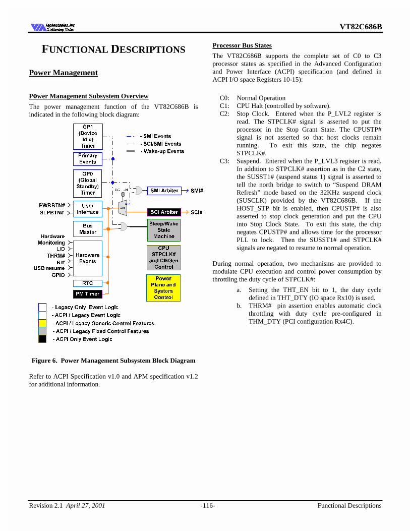
VT82C686B
Revision 2.1 April 27, 2001 -116- Functional Descriptions
7HFKQRORJLHV ,QF'HOLYHULQJ 9DOXH'HOLYHULQJ 9DOXH
FUNCTIONAL DESCRIPTIONS
Power Management
Power Management Subsystem Overview
The power management function of the VT82C686B is indicated in the following block diagram:
7+50
3RZHU
3ODQH DQG
6\VWHP
&RQWURO
*3
*OREDO
6WDQGE\
7LPHU
3:5%71
5,
60, $UELWHU
6OHHS:DNH
6WDWH
0DFKLQH
60,
6&,
/HJDF\ 2QO\ (YHQW /RJLF
$&3, /HJDF\ (YHQW /RJLF
$&3, 2QO\ (YHQW /RJLF
60, (YHQWV
6&,60, (YHQWV
'HF
&38
673&/.
DQG &ON*HQ
&RQWURO
*3
'HYLFH
,GOH
7LPHU
8VHU
,QWHUIDFH
+DUGZDUH
(YHQWV
57&
6&,B(1
$&3, /HJDF\ *HQHULF &RQWURO )HDWXUHV
$&3, /HJDF\ )L[HG &RQWURO )HDWXUHV
:DNHXS (YHQWV
30 7LPHU
6&, $UELWHU
%XV
0DVWHU
6/3%71
3ULPDU\
(YHQWV
86% UHVXPH
/,'
*3,2
+DUGZDUH
0RQLWRULQJ
Figure 6. Power Management Subsystem Block Diagram
Refer to ACPI Specification v1.0 and APM specification v1.2 for additional information.
Processor Bus States
The VT82C686B supports the complete set of C0 to C3 processor states as specified in the Advanced Configuration and Power Interface (ACPI) specification (and defined in ACPI I/O space Registers 10-15):
C0: Normal Operation C1: CPU Halt (controlled by software). C2: Stop Clock. Entered when the P_LVL2 register is
read. The STPCLK# signal is asserted to put the processor in the Stop Grant State. The CPUSTP# signal is not asserted so that host clocks remain running. To exit this state, the chip negates STPCLK#.
C3: Suspend. Entered when the P_LVL3 register is read. In addition to STPCLK# assertion as in the C2 state, the SUSST1# (suspend status 1) signal is asserted to tell the north bridge to switch to “Suspend DRAM Refresh” mode based on the 32KHz suspend clock (SUSCLK) provided by the VT82C686B. If the HOST_STP bit is enabled, then CPUSTP# is also asserted to stop clock generation and put the CPU into Stop Clock State. To exit this state, the chip negates CPUSTP# and allows time for the processor PLL to lock. Then the SUSST1# and STPCLK# signals are negated to resume to normal operation.
During normal operation, two mechanisms are provided to modulate CPU execution and control power consumption by throttling the duty cycle of STPCLK#:
a. Setting the THT_EN bit to 1, the duty cycle defined in THT_DTY (IO space Rx10) is used.
b. THRM# pin assertion enables automatic clock throttling with duty cycle pre-configured in THM_DTY (PCI configuration Rx4C).
VT82C686B
Revision 2.1 April 27, 2001 -117- Functional Descriptions
7HFKQRORJLHV ,QF'HOLYHULQJ 9DOXH'HOLYHULQJ 9DOXH
System Suspend States and Power Plane Control
There are three power planes inside the VT82C686B. The first power plane (VCCS) is always on unless turned off by the mechanical switch. The second power plane (VCC) is controlled by chip output SUSC# (also called “PSON”). The third plane (VCCRTC) is powered by the combination of the VCCS and the external battery (VBAT) for the integrated real time clock. Most of the circuitry inside the VT82C686B is powered by VCC. The amount of logic powered by VCCS is very small; its main function is to control the supply of VCC and other power planes. VCCRTC is always on unless both the mechanical switch and VBAT are removed.
The VT82C686B supports multiple system suspend states by configuring the SLP_TYP field of ACPI I/O space register Rx4-5:
a) POS (Power On Suspend): Most devices in the system remain powered. The host bus is put into an equivalent of the C3 state. In particular, the CPU is put into the Stop Grant State or Stop Clock State depending on the setting of the HOST_STP bit. SUSST1# is asserted to tell the north bridge to switch to “Suspend DRAM Refresh” mode based on the 32KHz SUSCLK provided by the VT82C686B. As to the PCI bus, setting the PCLK_RUN bit to 0 enables the CLKRUN protocol defined in the PCI Mobile Design Guide. That is, the PCKRUN# pin will be de-activated after the PCI bus is idle for 26 clocks. Any PCI bus masters including the north bridge may resume PCI clock operation by pulling the PCKRUN# pin low. During the PCKRUN# de-activation period, the PCISTP# pin may be activated to disable the output of the PCI clock generator if the PCI_STP bit is enabled. When the system resumes from POS, the VT82C686B can optionally resume without resetting the system, can reset the processor only, or can reset the entire system. When no reset is performed, the chip only needs to wait for the clock synthesizer and processor PLL to lock before the system is resumed, which typically takes 20ms.
b) STR (Suspend to RAM): Power is removed from most of the system except the system DRAM. Power is supplied to the suspend refresh logic in the north bridge (VTT of VT82C598) and the suspend logic of the VT82C686B (VCCS). The VT82C686B provides a 32KHz suspend clock to the north bridge for it to use to continue DRAM refresh.
c) STD (Suspend to Disk, also called Soft-off): Power is removed from most of the system except the suspend logic of VT82C686B (VCCS).
d) Mechanical Off: This is not a suspend state. All power in the system is removed except the RTC battery.
The suspend state is entered by setting the SLP_EN bit to 1. Three power plane control signals (SUSA#, SUSB# and
SUSC#) are provided to turn off more system power planes as the system moves to deeper power-down states, i.e., from normal operation to POS (only SUSA# asserted), to STR (both SUSA# and SUSB# asserted), and to STD (all three SUS# signals asserted). In particular, the assertion of SUSC# can be used to turn off the VCC supply to the VT82C686B.
One additional suspend status indicator (SUSST1#) is provided to inform the north bridge and the rest of the system of the processor and system suspend states. SUSST1# is asserted when the system enters the suspend state or the processor enters the C3 state. SUSST1# is connected to the north bridge to switch between normal and suspend-DRAM-refresh modes.
General Purpose I/O Ports
As ACPI compliant hardware, the VT82C686B includes PWRBTN#, SLPBTN#, and RI# pins to implement power button, sleep button, and ring indicator functionality, respectively. Furthermore, the VT82C686B offers many general-purpose I/O ports with the following capabilities:
• I2C/SMB Support • Thermal Detect • Notebook Lid Open/Close Detect • Battery Low Detect • Twelve General Purpose Input Ports (multiplexed with
other functions).
• Nineteen General Purpose Output Ports (1 dedicated and 18 multiplexed with other functions)
• Four General Purpose Input / Output Ports (multiplexed with other functions)
In addition, the VT82C686B provides an external dedicated SMI pin (EXTSMI#). The external SMI input can be programmed to trigger an SCI or SMI at both the rising and falling edges of the corresponding input signal. Software can check the status of the input pin and take appropriate actions.
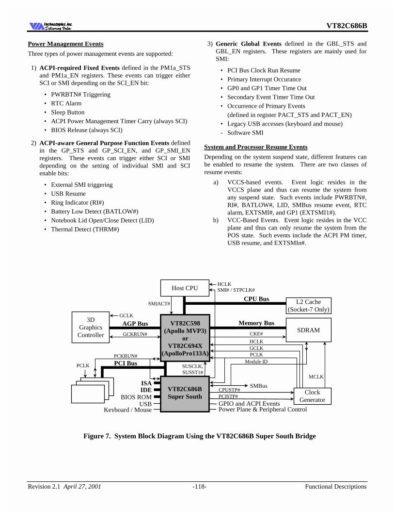
VT82C686B
Revision 2.1 April 27, 2001 -118- Functional Descriptions
7HFKQRORJLHV ,QF'HOLYHULQJ 9DOXH'HOLYHULQJ 9DOXH
Power Management Events
Three types of power management events are supported:
1) ACPI-required Fixed Events defined in the PM1a_STS and PM1a_EN registers. These events can trigger either SCI or SMI depending on the SCI_EN bit:
• PWRBTN# Triggering • RTC Alarm • Sleep Button • ACPI Power Management Timer Carry (always SCI) • BIOS Release (always SCI)
2) ACPI-aware General Purpose Function Events defined in the GP_STS and GP_SCI_EN, and GP_SMI_EN registers. These events can trigger either SCI or SMI depending on the setting of individual SMI and SCI enable bits:
• External SMI triggering • USB Resume • Ring Indicator (RI#) • Battery Low Detect (BATLOW#) • Notebook Lid Open/Close Detect (LID) • Thermal Detect (THRM#)
3) Generic Global Events defined in the GBL_STS and GBL_EN registers. These registers are mainly used for SMI:
• PCI Bus Clock Run Resume • Primary Interrupt Occurance • GP0 and GP1 Timer Time Out • Secondary Event Timer Time Out • Occurrence of Primary Events (defined in register PACT_STS and PACT_EN) • Legacy USB accesses (keyboard and mouse) - Software SMI
System and Processor Resume Events
Depending on the system suspend state, different features can be enabled to resume the system. There are two classes of resume events:
a) VCCS-based events. Event logic resides in the VCCS plane and thus can resume the system from any suspend state. Such events include PWRBTN#, RI#, BATLOW#, LID, SMBus resume event, RTC alarm, EXTSMI#, and GP1 (EXTSMI1#).
b) VCC-Based Events. Event logic resides in the VCC plane and thus can only resume the system from the POS state. Such events include the ACPI PM timer, USB resume, and EXTSMIn#.
PCKRUN# PCLK
HCLKGCLK
Host CPU
CPU Bus
CKE#
Memory Bus
SMBusISA
VT82C598(Apollo MVP3)
orVT82C694X
(ApolloPro133A)
SDRAM
3DGraphics
Controller
AGP Bus
PCISTP#
GPIO and ACPI EventsBIOS ROM
L2 Cache(Socket-7 Only)
GCKRUN#
PCI Bus
IDE
USBPower Plane & Peripheral Control
VT82C686BSuper South
Keyboard / Mouse
CPUSTP# ClockGenerator
MCLK
HCLK
GCLK
PCLK
SMI# / STPCLK#
SUSCLK,SUSST1#
SMIACT#
Module ID
Figure 7. System Block Diagram Using the VT82C686B Super South Bridge
VT82C686B
Revision 2.1 April 27, 2001 -119- Functional Descriptions
7HFKQRORJLHV ,QF'HOLYHULQJ 9DOXH'HOLYHULQJ 9DOXH
Legacy Power Management Timers
In addition to the ACPI power management timer, the VT82C686B includes the following four legacy power management timers:
GP0 Timer: general purpose timer with primary event
GP1 Timer: general purpose timer with peripheral event reload
Secondary Event Timer: to monitor secondary events
Conserve Mode Timer: Hardware-controlled return to standby
The normal sequence of operations for a general purpose timer (GP0 or GP1) is to
1) First program the time base and timer value of the initial count (register GP_TIM_CNT).
2) Then activate counting by setting the GP0_START or GP1_START bit to one: the timer will start with the initial count and count down towards 0.
3) When the timer counts down to zero, an SMI will be generated if enabled (GP0TO_EN and GP1TO_EN in the GBL_EN register) with status recorded (GP0TO_STS and GP1TO_STS in the GBL_STS register).
4) Each timer can also be programmed to reload the initial count and restart counting automatically after counting down to 0. This feature is not used in standard VIA BIOS.
The GP0 and GP1 timers can be used just as the general purpose timers described above. However, they can also be programmed to reload the initial count by system primary events or peripheral events thus used as primary event (global standby) timer and peripheral timer, respectively. The secondary event timer is solely used to monitor secondary events.
System Primary and Secondary Events
Primary system events are distinguished in the PRI_ACT_STS and PRI_ACT_EN registers:
Bit Event Trigger 7 Keyboard Access I/O port 60h 6 Serial Port Access I/O ports 3F8h-3FFh, 2F8h-2FFh,
3E8h-3EFh, or 2E8h-2EFh 5 Parallel Port Access I/O ports 378h-37Fh or 278h-27Fh 4 Video Access I/O ports 3B0h-3DFh or memory
A/B segments 3 IDE/Floppy Access I/O ports 1F0h-1F7h, 170h-177h,
or 3F5h 2 Reserved 1 Primary Interrupts Each channel of the interrupt
controller can be programmed to be a primary or secondary interrupt
0 ISA Master/DMA Activity Each category can be enabled as a primary event by setting the corresponding bit of the PRI_ACT_EN register to 1. If
enabled, the occurrence of the primary event reloads the GP0 timer if the PACT_GP0_EN bit is also set to 1. The cause of the timer reload is recorded in the corresponding bit of PRI_ACT_STS register while the timer is reloaded. If no enabled primary event occurs during the count down, the GP0 timer will time out (count down to 0) and the system can be programmed (setting the GP0TO_EN bit in the GBL_EN register to one) to trigger an SMI to switch the system to a power down mode.
The VT82C686B distinguishes two kinds of interrupt requests as far as power management is concerned: the primary and secondary interrupts. Like other primary events, the occurrence of a primary interrupt demands that the system be restored to full processing capability. Secondary interrupts, however, are typically used for housekeeping tasks in the background unnoticeable to the user. The VT82C686B allows each channel of interrupt request to be declared as either primary, secondary, or ignorable in the PIRQ_CH and SIRQ_CH registers. Secondary interrupts are the only system secondary events defined in the VT82C686B.
Like primary events, primary interrupts can be made to reload the GP0 timer by setting the PIRQ_EN bit to 1. Secondary interrupts do not reload the GP0 timer. Therefore the GP0 timer will time out and the SMI routine can put the system into power down mode if no events other than secondary interrupts are happening periodically in the background.
Primary events can be programmed to trigger an SMI (setting of the PACT_EN bit). Typically, this SMI triggering is turned off during normal system operation to avoid degrading system performance. Triggering is turned on by the SMI routine before entering the power down mode so that the system may be returned to normal operation at the occurrence of primary events. At the same time, the GP0 timer is reloaded and the count down process is restarted.
Peripheral Events
Primary and secondary events define system events in general and the response is typically expressed in terms of system events. Individual peripheral events can also be monitored by the VT82C686B through the GP1 timer. The following four categories of peripheral events are distinguished (via register GP_RLD_EN):
Bit-7 Keyboard Access Bit-6 Serial Port Access Bit-4 Video Access Bit-3 IDE/Floppy Access The four categories are subsets of the primary events as defined in PRI_ACT_EN and the occurrence of these events can be checked through a common register PRI_ACT_STS. As a peripheral timer, GP1 can be used to monitor one (or more than one) of the above four device types by programming the corresponding bit to one and the other bits to zero. Time out of the GP1 timer indicates no activity of the corresponding device type and appropriate action can be taken as a result.
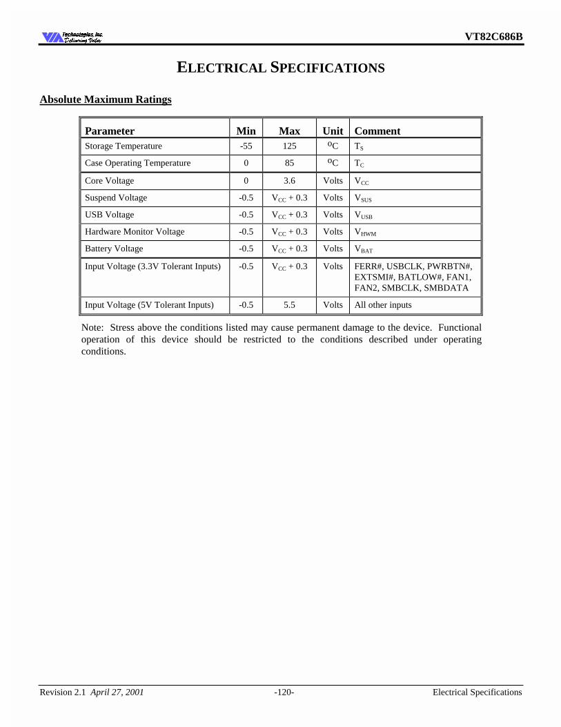
VT82C686B
Revision 2.1 April 27, 2001 -120- Electrical Specifications
7HFKQRORJLHV ,QF'HOLYHULQJ 9DOXH'HOLYHULQJ 9DOXH
ELECTRICAL SPECIFICATIONS
Absolute Maximum Ratings
Parameter Min Max Unit Comment Storage Temperature -55 125 oC TS
Case Operating Temperature 0 85 oC TC
Core Voltage 0 3.6 Volts VCC
Suspend Voltage -0.5 VCC + 0.3 Volts VSUS
USB Voltage -0.5 VCC + 0.3 Volts VUSB
Hardware Monitor Voltage -0.5 VCC + 0.3 Volts VHWM
Battery Voltage -0.5 VCC + 0.3 Volts VBAT
Input Voltage (3.3V Tolerant Inputs) -0.5 VCC + 0.3 Volts FERR#, USBCLK, PWRBTN#, EXTSMI#, BATLOW#, FAN1, FAN2, SMBCLK, SMBDATA
Input Voltage (5V Tolerant Inputs) -0.5 5.5 Volts All other inputs
Note: Stress above the conditions listed may cause permanent damage to the device. Functional operation of this device should be restricted to the conditions described under operating conditions.
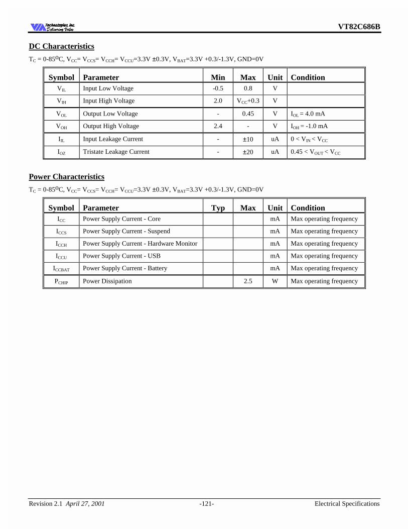
VT82C686B
Revision 2.1 April 27, 2001 -121- Electrical Specifications
7HFKQRORJLHV ,QF'HOLYHULQJ 9DOXH'HOLYHULQJ 9DOXH
DC Characteristics
TC = 0-85oC, VCC= VCCS= VCCH= VCCU=3.3V ±0.3V, VBAT=3.3V +0.3/-1.3V, GND=0V
Symbol Parameter Min Max Unit Condition VIL Input Low Voltage -0.5 0.8 V
VIH Input High Voltage 2.0 VCC+0.3 V
VOL Output Low Voltage - 0.45 V IOL = 4.0 mA
VOH Output High Voltage 2.4 - V IOH = -1.0 mA
IIL Input Leakage Current - ±10 uA 0 < VIN < VCC
IOZ Tristate Leakage Current - ±20 uA 0.45 < VOUT < VCC
Power Characteristics
TC = 0-85oC, VCC= VCCS= VCCH= VCCU=3.3V ±0.3V, VBAT=3.3V +0.3/-1.3V, GND=0V
Symbol Parameter Typ Max Unit Condition ICC Power Supply Current - Core mA Max operating frequency
ICCS Power Supply Current - Suspend mA Max operating frequency
ICCH Power Supply Current - Hardware Monitor mA Max operating frequency
ICCU Power Supply Current - USB mA Max operating frequency
ICCBAT Power Supply Current - Battery mA Max operating frequency
PCHIP Power Dissipation 2.5 W Max operating frequency
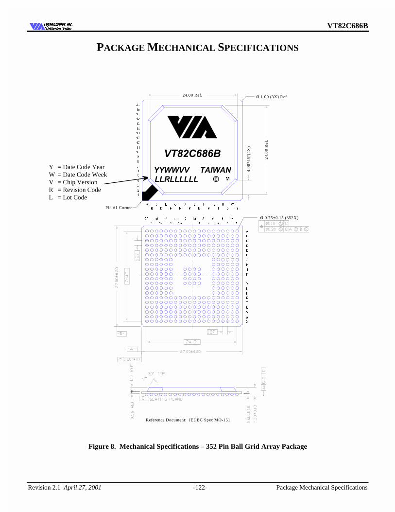
VT82C686B
Revision 2.1 April 27, 2001 -122- Package Mechanical Specifications
7HFKQRORJLHV ,QF'HOLYHULQJ 9DOXH'HOLYHULQJ 9DOXH
PACKAGE MECHANICAL SPECIFICATIONS
Figure 8. Mechanical Specifications – 352 Pin Ball Grid Array Package
=0
Y = Date Code Year W = Date Code Week V = Chip Version R = Revision Code L = Lot Code
Reference Document: JEDEC Spec MO-151
Ø 0.75±0.15 (352X)
4.00
*45°
(4X
)
24.0
0 R
ef.
Ø 1.00 (3X) Ref.
Pin #1 Corner
24.00 Ref.
<
:
9
8
7
5
3
1
0
/
.
-
+
*
)
(
'
&
%
$
;
:
9
8
7
5
*
)
(
'
+
-
.
/
0
1
3
$
%
&