Embed Size (px)
Citation preview
112/14/2010
PCB COST
DRIVERS
2
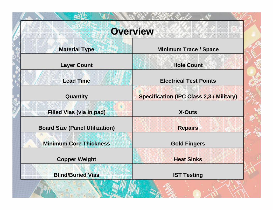
OverviewOverviewMaterial Type Minimum Trace / Space
Layer Count Hole Count
Lead Time Electrical Test Points
Quantity Specification (IPC Class 2,3 / Military)
Filled Vias (via in pad) X-Outs
Board Size (Panel Utilization) Repairs
Minimum Core Thickness Gold Fingers
Copper Weight Heat Sinks
Blind/Buried Vias IST Testing
3
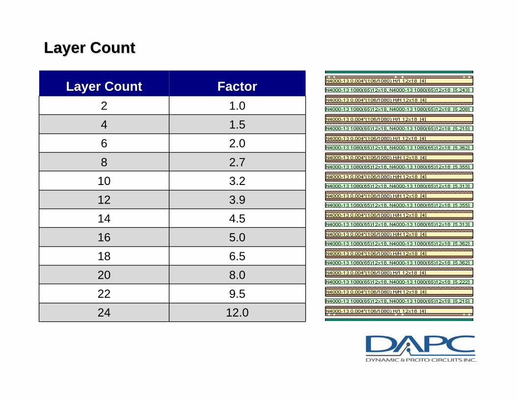
Layer CountLayer Count
Layer Count Factor2 1.04 1.56 2.08 2.7
10 3.212 3.914 4.516 5.018 6.520 8.022 9.524 12.0
4
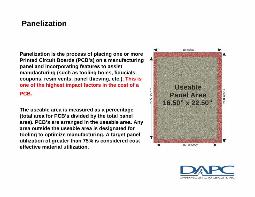
Panelization
Panelization is the process of placing one or more Printed Circuit Boards (PCB’s) on a manufacturing panel and incorporating features to assist manufacturing (such as tooling holes, fiducials, coupons, resin vents, panel thieving, etc.). This is one of the highest impact factors in the cost of a PCB.
The useable area is measured as a percentage (total area for PCB’s divided by the total panel area). PCB’s are arranged in the useable area. Any area outside the useable area is designated for tooling to optimize manufacturing. A target panel utilization of greater than 75% is considered cost effective material utilization.
Useable Panel Area
16.50” x 22.50”
18 inches
16.50 inches
22.5
0 inc
hes
24.0
inch
es
5
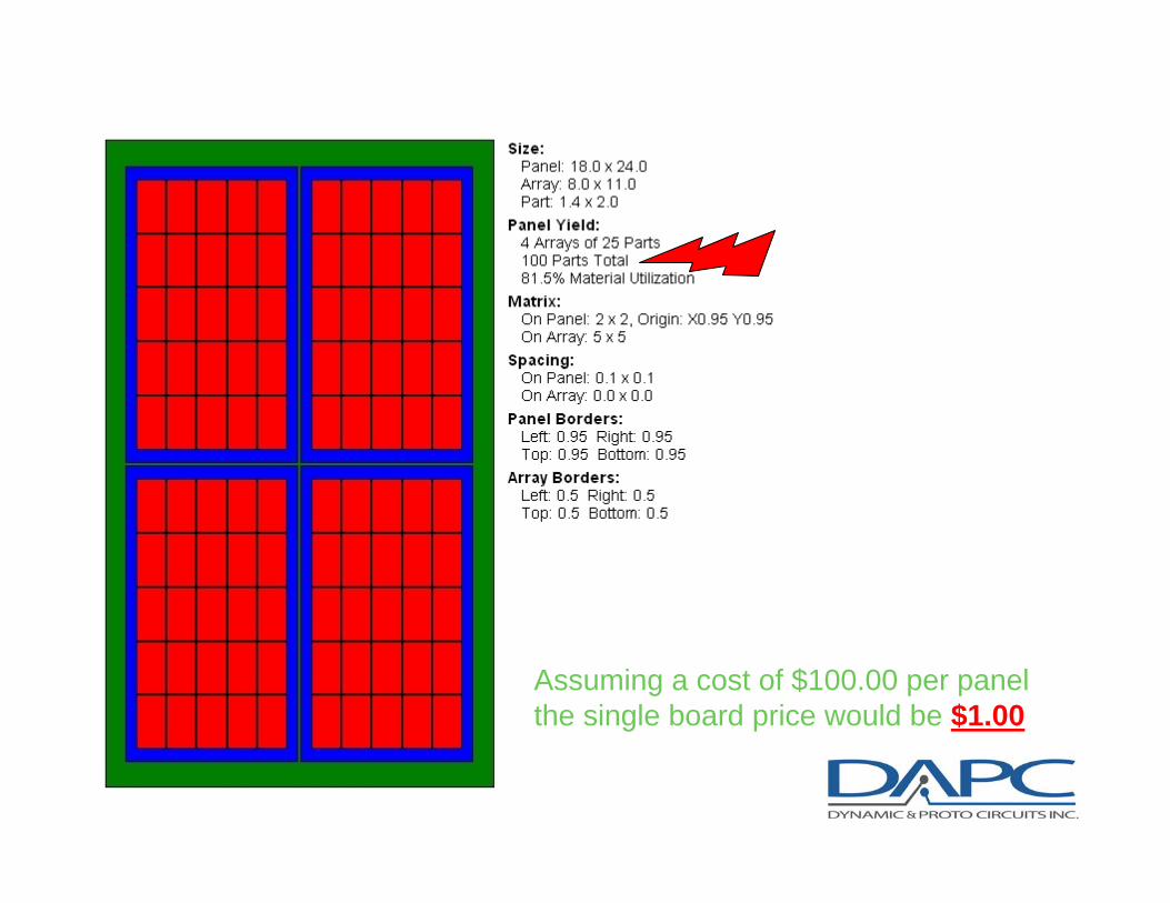
Assuming a cost of $100.00 per panel the single board price would be $1.00
6
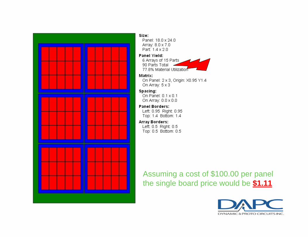
Assuming a cost of $100.00 per panel the single board price would be $1.11
7
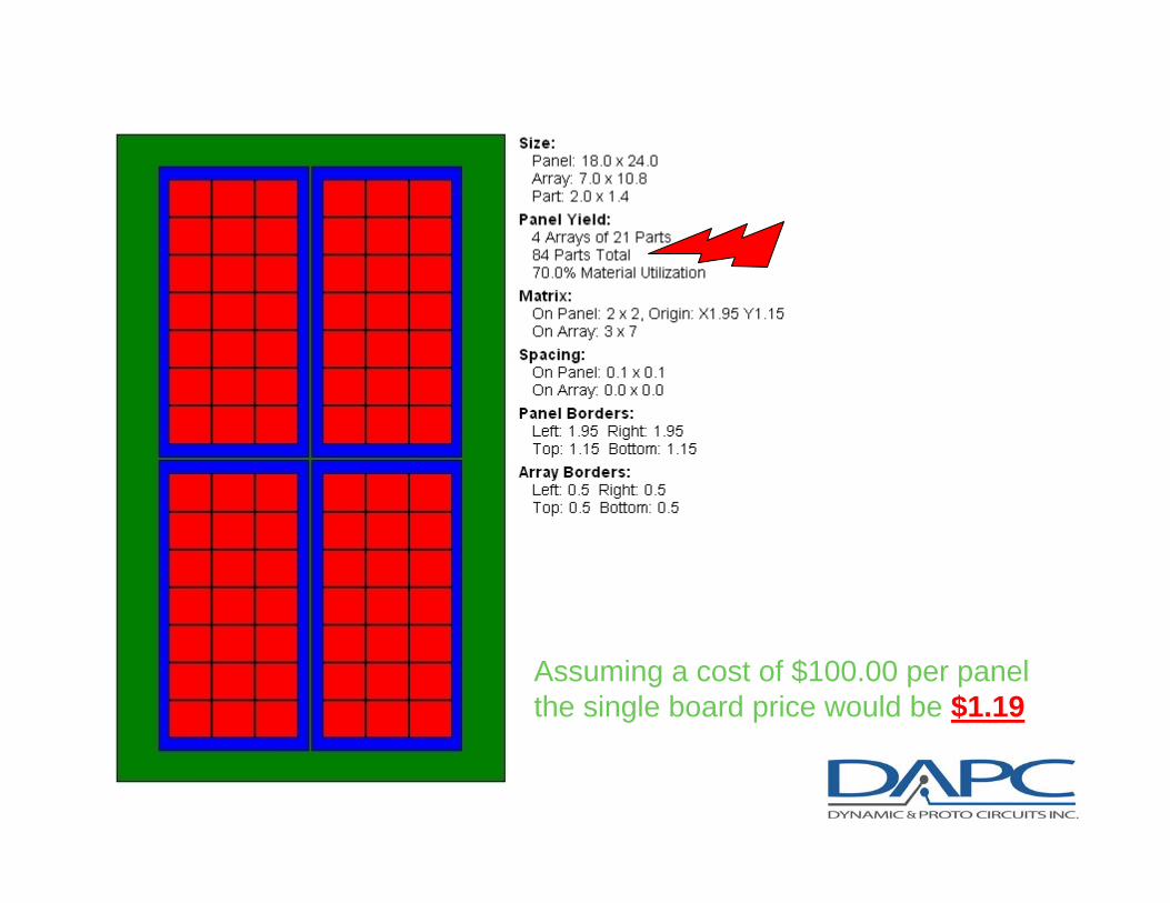
Assuming a cost of $100.00 per panel the single board price would be $1.19
8
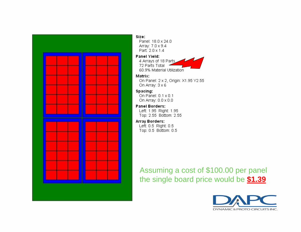
Assuming a cost of $100.00 per panel the single board price would be $1.39
9
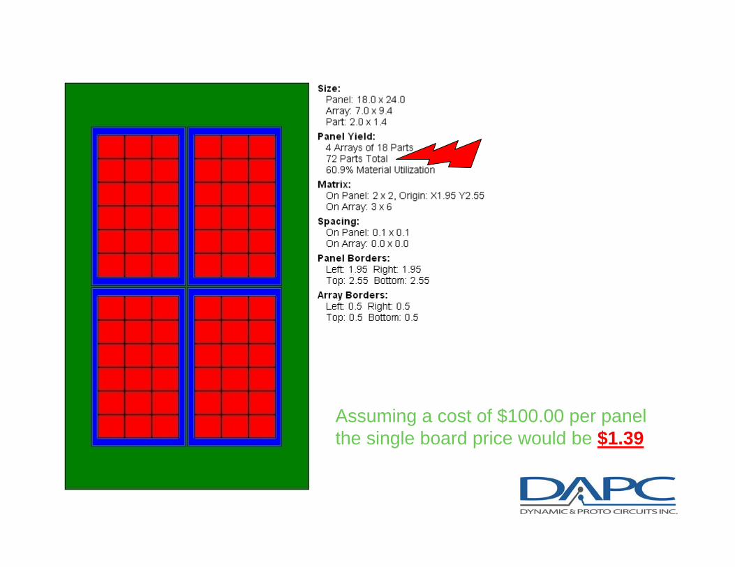
Assuming a cost of $100.00 per panel the single board price would be $1.39
10
Material TypeMaterial Type FactorFactor
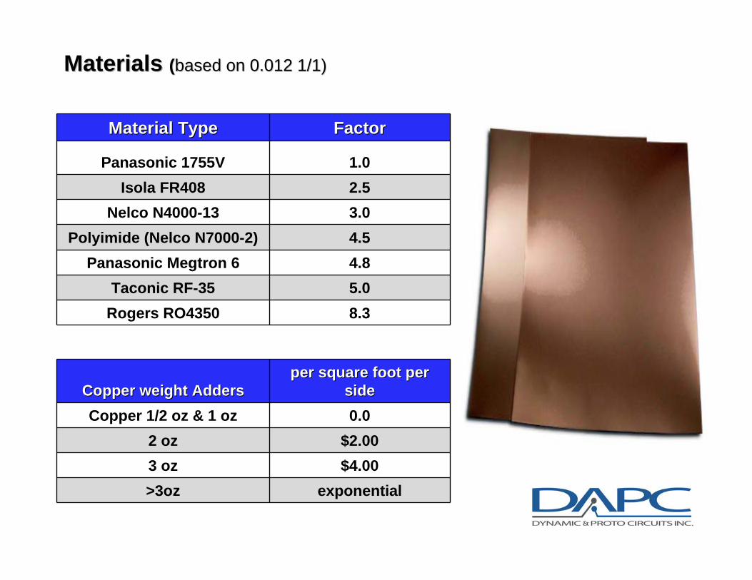
Panasonic 1755V 1.0Isola FR408 2.5
Nelco N4000-13 3.0Polyimide (Nelco N7000-2) 4.5
Panasonic Megtron 6 4.8Taconic RF-35 5.0
Rogers RO4350 8.3
Copper weight AddersCopper weight Addersper square foot per per square foot per
sidesideCopper 1/2 oz & 1 oz 0.0
2 oz $2.003 oz $4.00>3oz exponential
Materials Materials ((based on 0.012 1/1)based on 0.012 1/1)
11
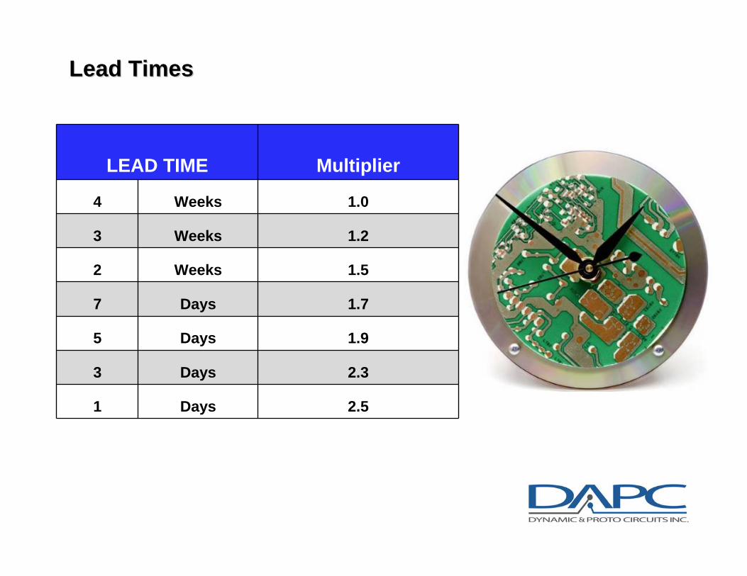
LEAD TIME Multiplier
4 Weeks 1.0
3 Weeks 1.2
2 Weeks 1.5
7 Days 1.7
5 Days 1.9
3 Days 2.3
1 Days 2.5
Lead TimesLead Times
12
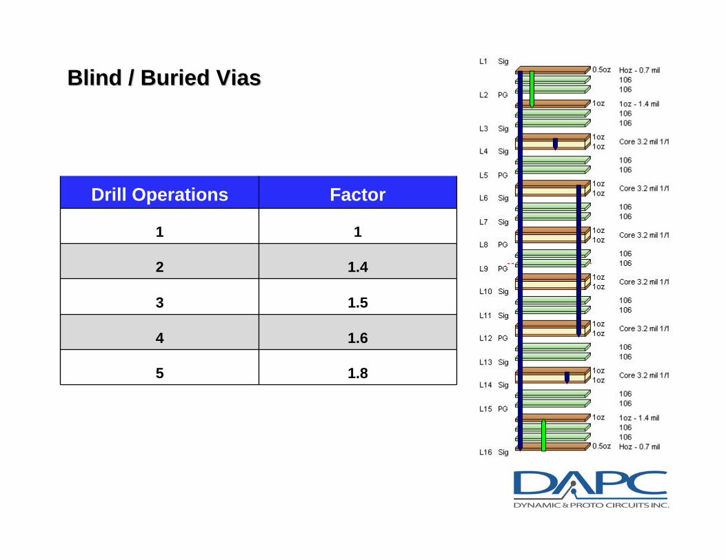
Drill Operations Factor
1 1
2 1.4
3 1.5
4 1.6
5 1.8
Blind / Buried ViasBlind / Buried Vias
13
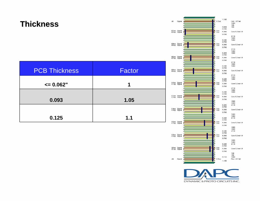
ThicknessThickness
PCB Thickness Factor
<= 0.062" 1
0.093 1.05
0.125 1.1
14
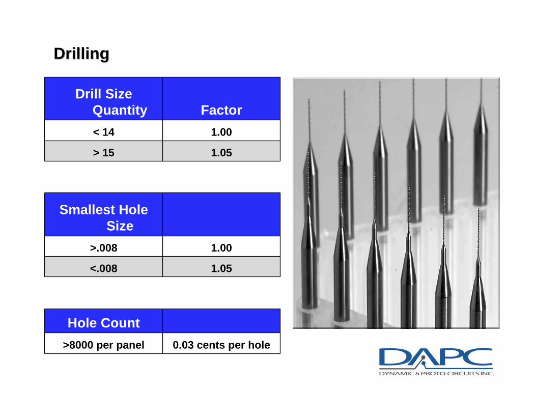
DrillingDrilling
Drill Size Quantity Factor< 14 1.00
> 15 1.05
Smallest Hole Size
>.008 1.00
<.008 1.05
Hole Count>8000 per panel 0.03 cents per hole
15
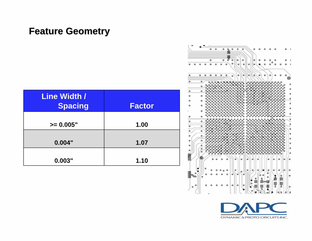
Line Width / Spacing Factor
>= 0.005" 1.00
0.004" 1.07
0.003" 1.10
Feature GeometryFeature Geometry
16
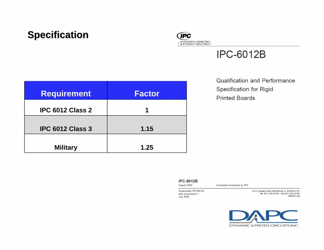
SpecificationSpecification
Requirement Factor
IPC 6012 Class 2 1
IPC 6012 Class 3 1.15
Military 1.25
17
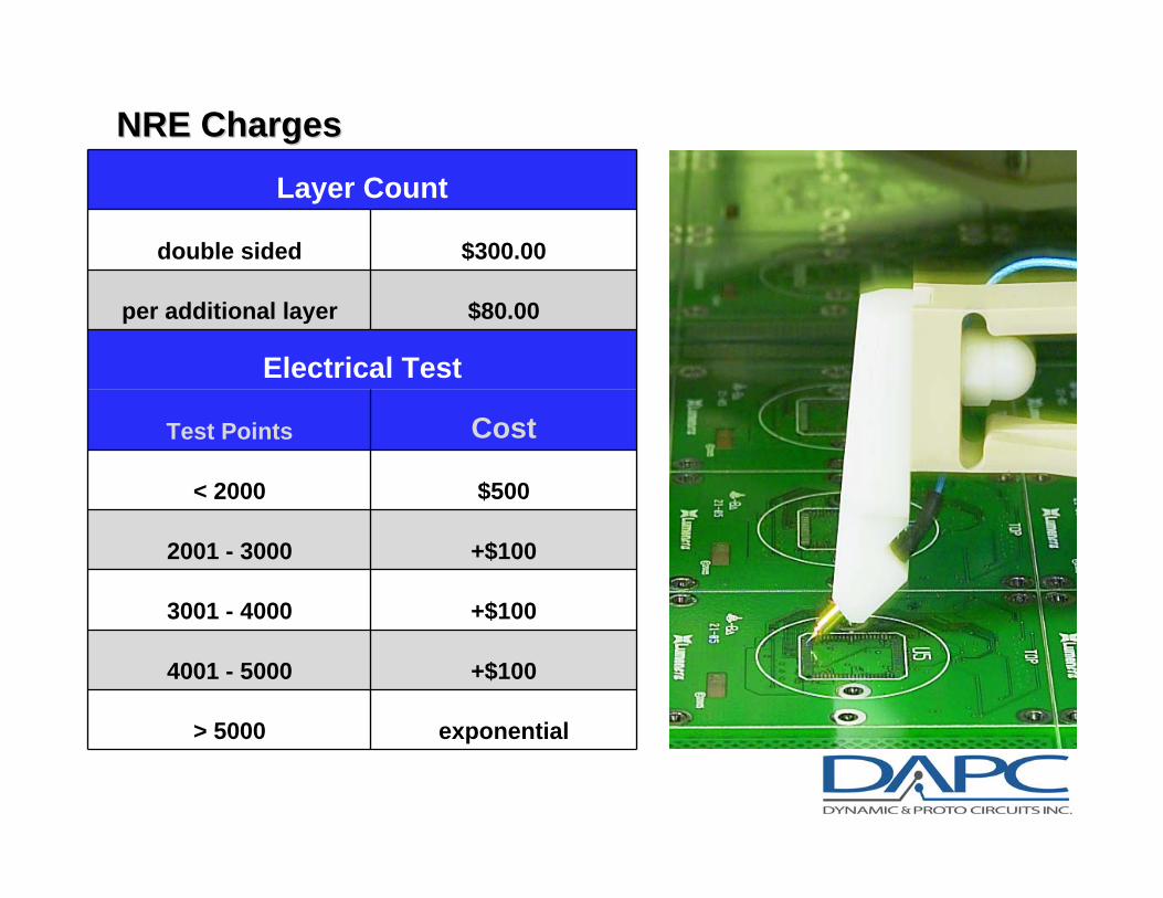
Layer Count
double sided $300.00
per additional layer $80.00
Electrical Test
Test Points Cost
< 2000 $500
2001 - 3000 +$100
3001 - 4000 +$100
4001 - 5000 +$100
> 5000 exponential
NRE ChargesNRE Charges
18
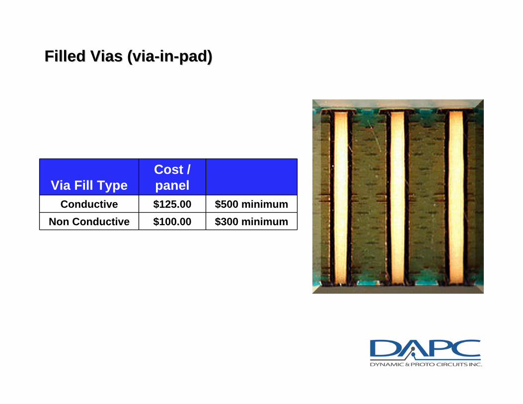
Via Fill TypeCost / panel
Conductive $125.00 $500 minimumNon Conductive $100.00 $300 minimum
Filled Vias (viaFilled Vias (via--inin--pad)pad)
19
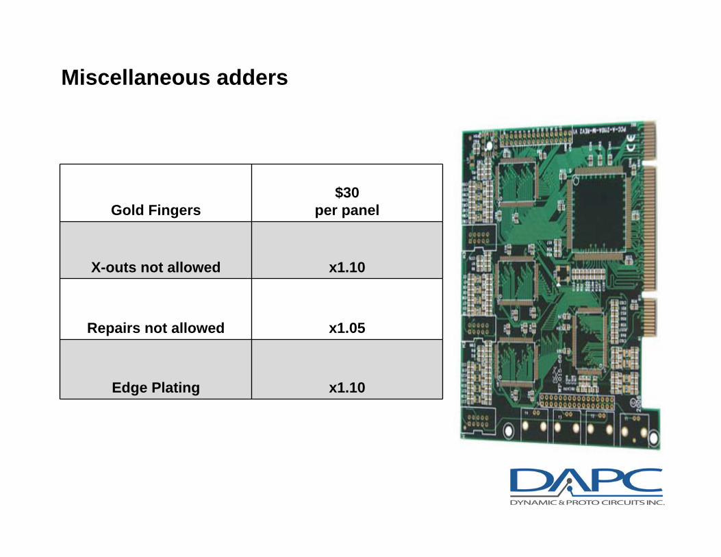
Miscellaneous adders
Gold Fingers$30
per panel
X-outs not allowed x1.10
Repairs not allowed x1.05
Edge Plating x1.10
20
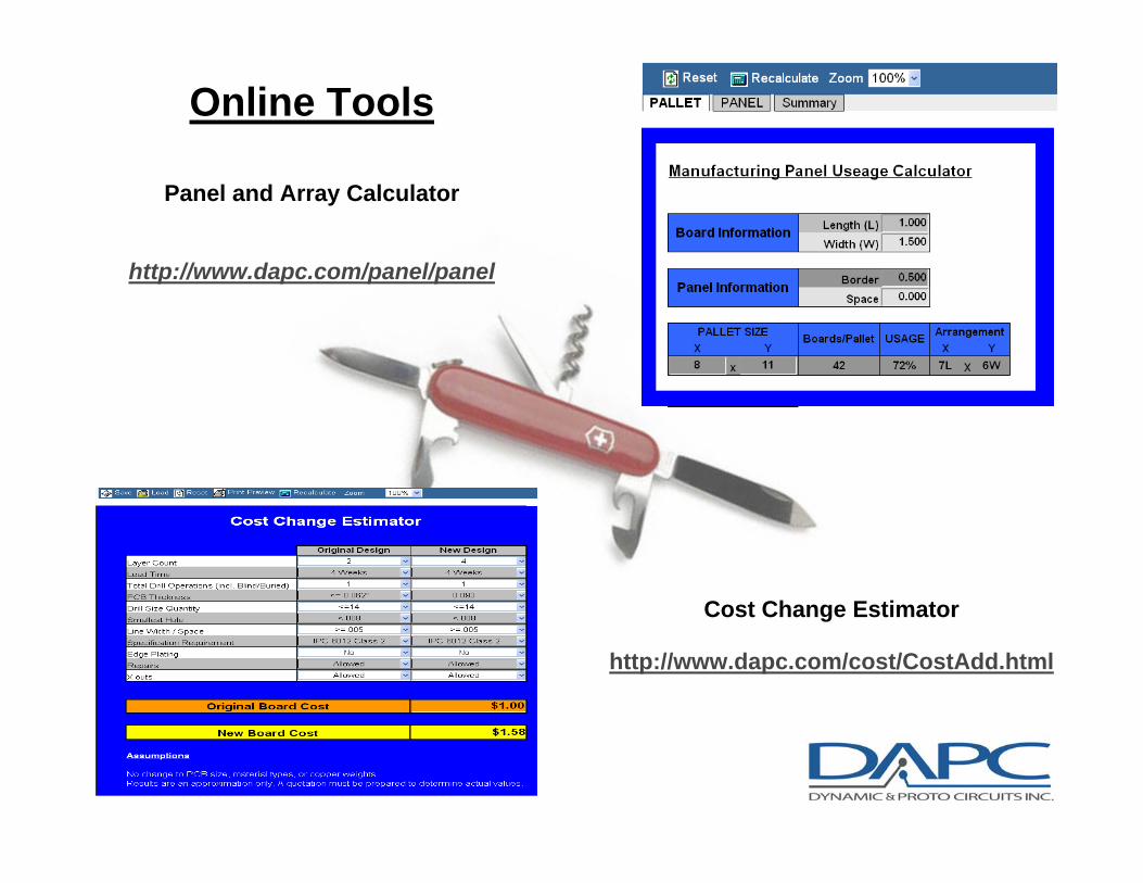
Online Tools
Cost Change Estimator
http://www.dapc.com/cost/CostAdd.html
http://www.dapc.com/panel/panel
Panel and Array Calculator